InnoSwitch3-CE Family www.power.com September 2017 Off-Line CV/CC QR Flyback Switcher IC with Integrated 650 V MOSFET, Synchronous Rectification & FluxLink Feedback. For Applications up to 65 W This Product is Covered by Patents and/or Pending Patent Applications. Product Highlights Highly Integrated, Compact Footprint • Up to 94% efficiency across full load range • Incorporates a multi-mode Quasi-Resonant (QR) / CCM flyback controller, 650 V MOSFET, secondary-side sensing and synchronous rectification driver • Integrated FluxLink™, HIPOT-isolated, feedback link • Exceptional CV/CC accuracy, independent of external components • Adjustable accurate output current sense using external sense resistor EcoSmart™ – Energy Efficient • Less than 15 mW no-load including line sense • Easily meets all global energy efficiency regulations • Low heat dissipation Advanced Protection / Safety Features • Secondary MOSFET or diode short-circuit protection • Open SR FET-gate detection • Fast input line UV/OV protection Optional Features • Cable-drop compensation with multiple settings • Variable output voltage, constant current profiles • Auto-restart or latching fault response for output OVP/UVP • Multiple output UV fault thresholds • Latching or hysteretic primary over-temperature protection Full Safety and Regulatory Compliance • Reinforced isolation • Isolation voltage >4000 VAC • 100% production HIPOT testing • UL1577 and TUV (EN60950) safety approved • Excellent noise immunity enables designs that achieve class “A” performance criteria for EN61000-4 suite; EN61000-4-2, 4-3 (30 V/m), 4-4, 4-5, 4-6, 4-8 (100 A/m) and 4-9 (1000 A/m) and Ford FMC1278 (RI-115) Green Package • Halogen free and RoHS compliant Applications • High efficiency flyback designs up to 65 W • High current charger and adaptors for mobile devices • Consumer electronics − set-top boxes, networking, gaming, LED Description The InnoSwitch™3-CE family of ICs dramatically simplifies the design and manufacture of flyback power converters, particularly those requiring high efficiency and/or compact size. The InnoSwitch3-CE family incorporates primary and secondary controllers and safety-rated feedback into a single IC. InnoSwitch3-CE family devices incorporate multiple protection features including line over and under-voltage protection, output over-voltage and over-current limiting, and over-temperature shutdown. Devices are available that support the common combinations of latching and auto-restart behaviors required by applications such as chargers, adapters, consumer electronics and industrial systems. The devices are available with and without cable-drop compensation. Figure 1. Typical Application schematic. Output Power Table Product 3 230 VAC ± 15% 85-265 VAC Adapter 1 Open Frame 2 Adapter 1 Open Frame 2 INN3162C 10 W 12 W 10 W 10 W INN3163C 12 W 15 W 12 W 12 W INN3164C 20 W 25 W 15 W 20 W INN3165C 25 W 30 W 22 W 25 W INN3166C 35 W 40 W 27 W 36 W INN3167C 45 W 50 W 40 W 45 W INN3168C 55 W 65 W 50 W 55 W Table 1. Output Power Table. Notes: 1. Minimum continuous power in a typical non-ventilated enclosed typical size adapter measured at 40 °C ambient. Max output power is dependent on the design. With condition that package temperature must be < 125 °C. 2. Minimum peak power capability. 3. Package: InSOP-24D. Figure 2. High Creepage, Safety-Compliant InSOP-24D Package. Secondary Control IC SR FET D V S IS VOUT BPS FB GND SR BPP FWD Primary FET and Controller InnoSwitch3-CE
Transcript
InnoSwitch3-CE Family
www.power.com September 2017
Off-Line CV/CC QR Flyback Switcher IC with Integrated 650 V MOSFET, Synchronous Rectification & FluxLink Feedback. For Applications up to 65 W
This Product is Covered by Patents and/or Pending Patent Applications.
Product HighlightsHighly Integrated, Compact Footprint• Up to 94% efficiency across full load range• Incorporates a multi-mode Quasi-Resonant (QR) / CCM flyback
controller, 650 V MOSFET, secondary-side sensing and synchronousrectification driver
• Integrated FluxLink™, HIPOT-isolated, feedback link• Exceptional CV/CC accuracy, independent of external components• Adjustable accurate output current sense using external sense resistor
EcoSmart™ – Energy Efficient• Less than 15 mW no-load including line sense• Easily meets all global energy efficiency regulations• Low heat dissipation
Advanced Protection / Safety Features• Secondary MOSFET or diode short-circuit protection• Open SR FET-gate detection• Fast input line UV/OV protection
Optional Features• Cable-drop compensation with multiple settings• Variable output voltage, constant current profiles• Auto-restart or latching fault response for output OVP/UVP• Multiple output UV fault thresholds• Latching or hysteretic primary over-temperature protection
Full Safety and Regulatory Compliance• Reinforced isolation• Isolation voltage >4000 VAC• 100% production HIPOT testing• UL1577 and TUV (EN60950) safety approved• Excellent noise immunity enables designs that achieve class “A”
performance criteria for EN61000-4 suite; EN61000-4-2, 4-3 (30V/m), 4-4, 4-5, 4-6, 4-8 (100 A/m) and 4-9 (1000 A/m) and FordFMC1278 (RI-115)
Green Package• Halogen free and RoHS compliant
Applications• High efficiency flyback designs up to 65 W• High current charger and adaptors for mobile devices• Consumer electronics − set-top boxes, networking, gaming, LED
DescriptionThe InnoSwitch™3-CE family of ICs dramatically simplifies the design and manufacture of flyback power converters, particularly those requiring high efficiency and/or compact size. The InnoSwitch3-CE family incorporates primary and secondary controllers and safety-rated feedback into a single IC.
InnoSwitch3-CE family devices incorporate multiple protection features including line over and under-voltage protection, output over-voltage and over-current limiting, and over-temperature shutdown. Devices are available that support the common combinations of latching and auto-restart behaviors required by applications such as chargers, adapters, consumer electronics and industrial systems. The devices are available with and without cable-drop compensation.
Figure 1. Typical Application schematic.
Output Power Table
Product3
230 VAC ± 15% 85-265 VAC
Adapter1 Open Frame2 Adapter1 Open
Frame2
INN3162C 10 W 12 W 10 W 10 W
INN3163C 12 W 15 W 12 W 12 W
INN3164C 20 W 25 W 15 W 20 W
INN3165C 25 W 30 W 22 W 25 W
INN3166C 35 W 40 W 27 W 36 W
INN3167C 45 W 50 W 40 W 45 W
INN3168C 55 W 65 W 50 W 55 W
Table 1. Output Power Table.Notes: 1. Minimum continuous power in a typical non-ventilated enclosed typical size
adapter measured at 40 °C ambient. Max output power is dependent on thedesign. With condition that package temperature must be < 125 °C.
2. Minimum peak power capability.3. Package: InSOP-24D.
Figure 2. High Creepage, Safety-Compliant InSOP-24D Package.
ISENSE (IS) Pin (Pin 1)Connection to the power supply output terminals. An external current sense resistor should be connected between this and the GND pin. If current regulation is not required, this pin should be tied to the GND pin.
SECONDARY GROUND (GND) (Pin 2)GND for the secondary IC. Note this is not the power supply output GND due to the presence of the sense resistor between this and the ISENSE pin.
FEEDBACK (FB) Pin (Pin 3)Connection to an external resistor divider to set the power supply output voltage.
SECONDARY BYPASS (BPS) Pin (Pin 4)Connection point for an external bypass capacitor for the secondary IC supply.
SYNCHRONOUS RECTIFIER DRIVE (SR) Pin (Pin 5)Gate driver for external SR FET. If no SR FET is used connect this pin to GND.
OUTPUT VOLTAGE (VOUT) Pin (Pin 6)Connected directly to the output voltage, to provide current for the controller on the secondary-side and provide secondary protection.
FORWARD (FWD) Pin (Pin 7)The connection point to the switching node of the transformer output winding providing information on primary switch timing. Provides power for the secondary-side controller when VOUT is below threshold.
NC Pin (Pin 8-12)Leave open. Should not be connected to any other pins.
UNDER/OVER INPUT VOLTAGE (V) Pin (Pin 13)A high-voltage pin connected to the AC or DC side of the input bridge for detecting undervoltage and overvoltage conditions at the power supply input. This pin should be tied to GND to disable UV/OV protection.
PRIMARY BYPASS (BPP) Pin (Pin 14)The connection point for an external bypass capacitor for the primary-side supply. This is also the ILIM selection pin for choosing standard ILIM or ILIM+1.
NC Pin (Pin 15)Leave open. Should not be connected to any other pins.
SOURCE (S) Pin (Pin 16-19)These pins are the power MOSFET source connection. Also ground reference for primary BYPASS pin.
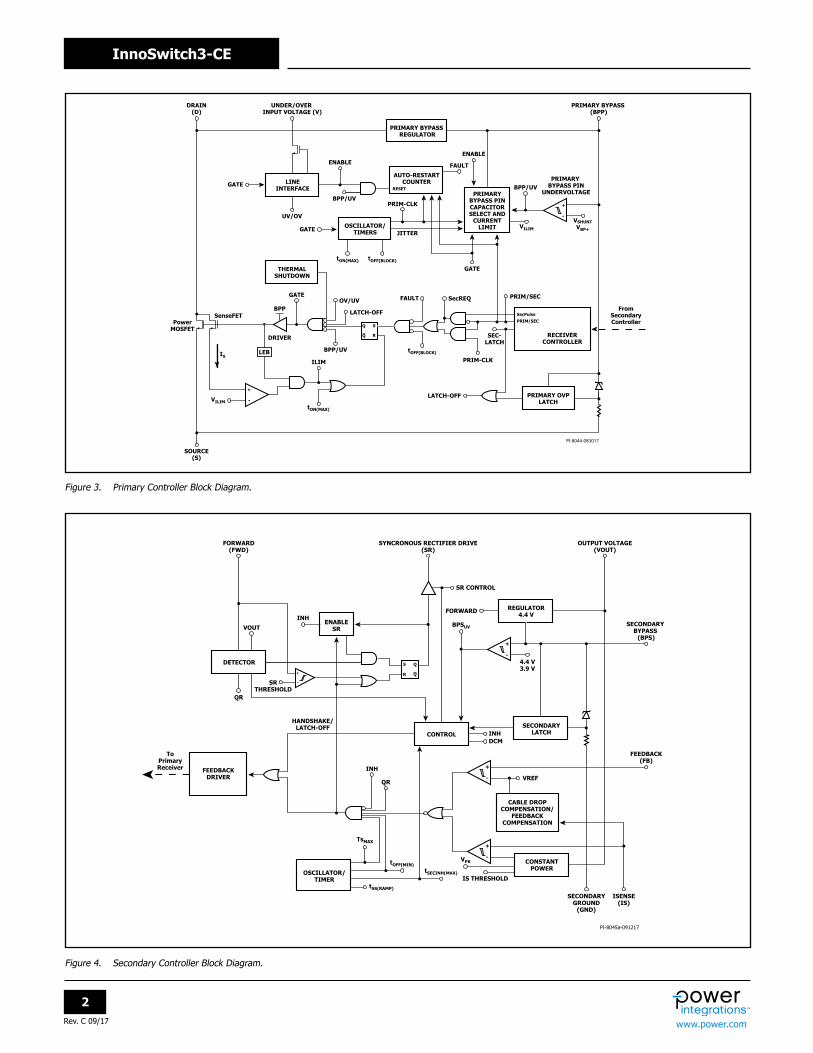
InnoSwitch3-CE Functional DescriptionThe InnoSwitch3-CE combines a high-voltage power MOSFET switch, along with both primary-side and secondary-side controllers in one device.
The architecture incorporates a novel inductive coupling feedback scheme (FluxLink) using the package lead frame and bond wires to provide a safe, reliable, and cost-effective means to transmit accurate, output voltage and current information from the secondary controller to the primary controller.
The primary controller on InnoSwitch3-CE is a Quasi-Resonant (QR) flyback controller that has the ability to operate in continuous conduction mode (CCM), boundary mode (CrM) and discontinuous conduction mode (DCM). The controller uses both variable frequency and variable current control schemes. The primary controller consists of a frequency jitter oscillator, a receiver circuit magnetically coupled to the secondary controller, a current limit controller, 5 V regulator on the PRIMARY BYPASS pin, audible noise reduction engine for light load operation, bypass overvoltage detection circuit, a lossless input line sensing circuit, current limit selection circuitry, over-temperature protection, leading edge blanking, secondary output diode / SR FET short protection circuit and a 650 V / 725 V power MOSFET.
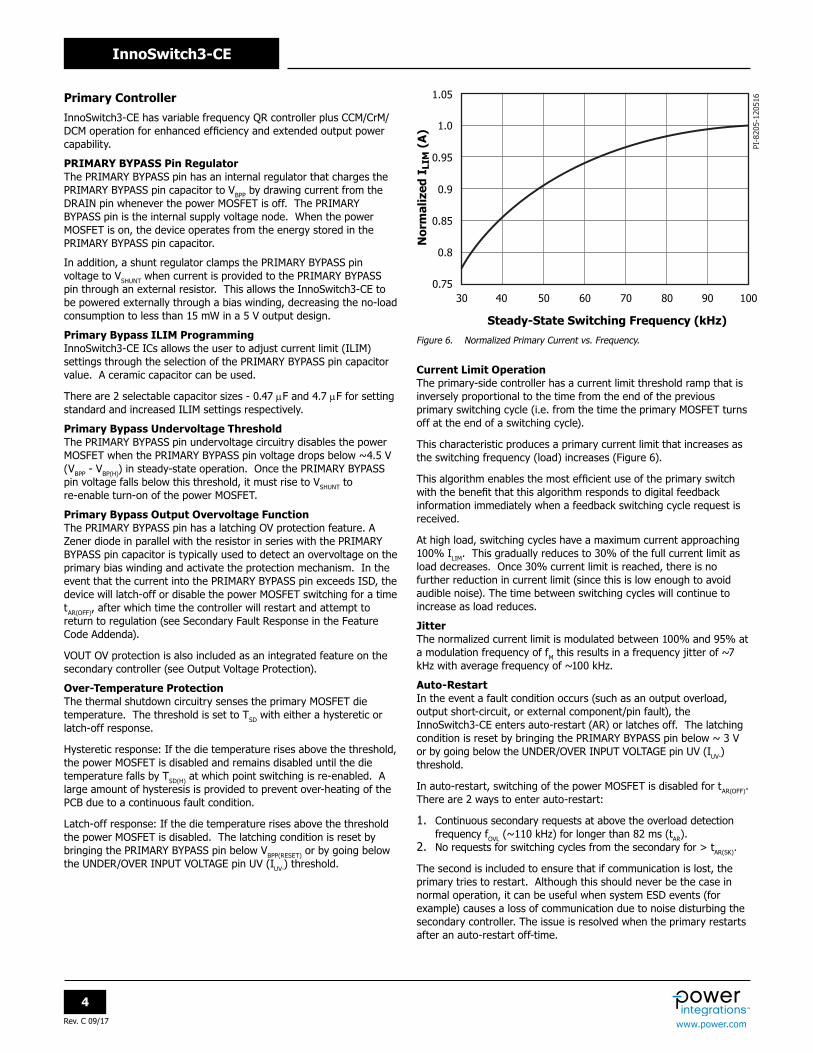
The InnoSwitch3-CE secondary controller consists of a transmitter circuit that is magnetically coupled to the primary receiver, a constant voltage (CV) and a constant current (CC) control circuit, a 4.4 V regulator on the SECONDARY BYPASS pin, synchronous rectifier FET driver, QR mode circuit, oscillator and timing circuit, and numerous integrated protection features.
Figure 3 and Figure 4 show the functional block diagrams of the primary and secondary controller, highlighting the most important features.
InnoSwitch3-CE has variable frequency QR controller plus CCM/CrM/DCM operation for enhanced efficiency and extended output power capability.
PRIMARY BYPASS Pin RegulatorThe PRIMARY BYPASS pin has an internal regulator that charges the PRIMARY BYPASS pin capacitor to VBPP by drawing current from the DRAIN pin whenever the power MOSFET is off. The PRIMARY BYPASS pin is the internal supply voltage node. When the power MOSFET is on, the device operates from the energy stored in the PRIMARY BYPASS pin capacitor.
In addition, a shunt regulator clamps the PRIMARY BYPASS pin voltage to VSHUNT when current is provided to the PRIMARY BYPASS pin through an external resistor. This allows the InnoSwitch3-CE to be powered externally through a bias winding, decreasing the no-load consumption to less than 15 mW in a 5 V output design.
Primary Bypass ILIM ProgrammingInnoSwitch3-CE ICs allows the user to adjust current limit (ILIM) settings through the selection of the PRIMARY BYPASS pin capacitor value. A ceramic capacitor can be used.
There are 2 selectable capacitor sizes - 0.47 mF and 4.7 mF for setting standard and increased ILIM settings respectively.
Primary Bypass Undervoltage ThresholdThe PRIMARY BYPASS pin undervoltage circuitry disables the power MOSFET when the PRIMARY BYPASS pin voltage drops below ~4.5 V (VBPP - VBP(H)) in steady-state operation. Once the PRIMARY BYPASS pin voltage falls below this threshold, it must rise to VSHUNT to re-enable turn-on of the power MOSFET.
Primary Bypass Output Overvoltage FunctionThe PRIMARY BYPASS pin has a latching OV protection feature. A Zener diode in parallel with the resistor in series with the PRIMARY BYPASS pin capacitor is typically used to detect an overvoltage on the primary bias winding and activate the protection mechanism. In the event that the current into the PRIMARY BYPASS pin exceeds ISD, the device will latch-off or disable the power MOSFET switching for a time tAR(OFF), after which time the controller will restart and attempt to return to regulation (see Secondary Fault Response in the Feature Code Addenda).
VOUT OV protection is also included as an integrated feature on the secondary controller (see Output Voltage Protection).
Over-Temperature ProtectionThe thermal shutdown circuitry senses the primary MOSFET die temperature. The threshold is set to TSD with either a hysteretic or latch-off response.
Hysteretic response: If the die temperature rises above the threshold, the power MOSFET is disabled and remains disabled until the die temperature falls by TSD(H) at which point switching is re-enabled. A large amount of hysteresis is provided to prevent over-heating of the PCB due to a continuous fault condition.
Latch-off response: If the die temperature rises above the threshold the power MOSFET is disabled. The latching condition is reset by bringing the PRIMARY BYPASS pin below VBPP(RESET) or by going below the UNDER/OVER INPUT VOLTAGE pin UV (IUV-) threshold.
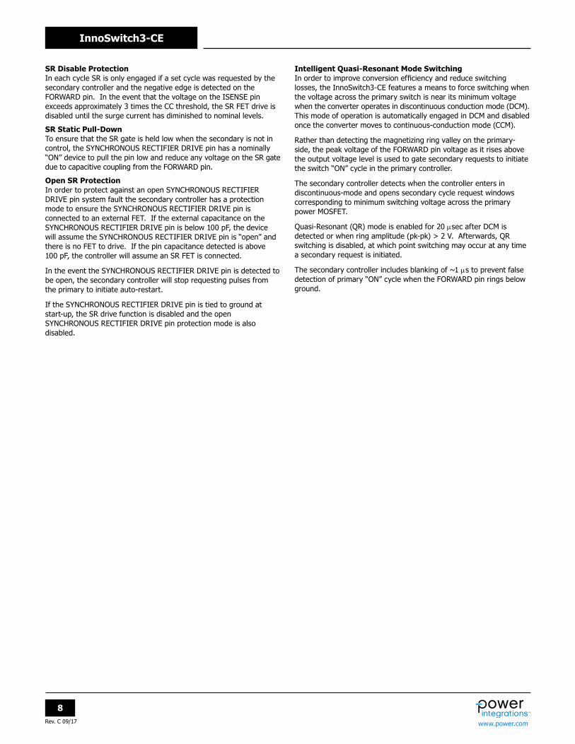
Current Limit OperationThe primary-side controller has a current limit threshold ramp that is inversely proportional to the time from the end of the previous primary switching cycle (i.e. from the time the primary MOSFET turns off at the end of a switching cycle).
This characteristic produces a primary current limit that increases as the switching frequency (load) increases (Figure 6).
This algorithm enables the most efficient use of the primary switch with the benefit that this algorithm responds to digital feedback information immediately when a feedback switching cycle request is received.
At high load, switching cycles have a maximum current approaching 100% ILIM. This gradually reduces to 30% of the full current limit as load decreases. Once 30% current limit is reached, there is no further reduction in current limit (since this is low enough to avoid audible noise). The time between switching cycles will continue to increase as load reduces.
JitterThe normalized current limit is modulated between 100% and 95% at a modulation frequency of fM this results in a frequency jitter of ~7 kHz with average frequency of ~100 kHz.
Auto-RestartIn the event a fault condition occurs (such as an output overload, output short-circuit, or external component/pin fault), the InnoSwitch3-CE enters auto-restart (AR) or latches off. The latching condition is reset by bringing the PRIMARY BYPASS pin below ~ 3 V or by going below the UNDER/OVER INPUT VOLTAGE pin UV (IUV-) threshold.
In auto-restart, switching of the power MOSFET is disabled for tAR(OFF). There are 2 ways to enter auto-restart:
1. Continuous secondary requests at above the overload detection frequency fOVL (~110 kHz) for longer than 82 ms (tAR).
2. No requests for switching cycles from the secondary for > tAR(SK).
The second is included to ensure that if communication is lost, the primary tries to restart. Although this should never be the case in normal operation, it can be useful when system ESD events (for example) causes a loss of communication due to noise disturbing the secondary controller. The issue is resolved when the primary restarts after an auto-restart off-time.
Figure 6. Normalized Primary Current vs. Frequency.
The first auto-restart off-time is short (tAR(OFF)SH). This short auto-restart time is to provide quick recovery under fast reset conditions. The short auto-restart off-time allows the controller to quickly check to determine whether the auto-restart condition is maintained beyond tAR(OFF)SH. If so it will resort to a full auto-restart off-time.
The auto-restart is reset as soon as an AC reset occurs.
SOA ProtectionIn the event that there are two consecutive cycles where the ILIM is reached within ~500 ns (the blanking time + current limit delay time), the controller will skip 2.5 cycles or ~25 ms (based on full frequency of 100 kHz). This provides sufficient time for the transformer to reset with large capacitive loads without extending the start-up time.
Secondary Rectifier/SR MOSFET Short Protection (SRS)In the event that the output diode or SR FET is short-circuited before or during the primary conduction cycle, the drain current (prior to the end of the leading edge blanking time) can be much higher than the maximum current limit threshold. If the controller turns the high-voltage power MOSFET off, the resulting peak drain voltage could exceed the rated BVDSS of the device, resulting in catastrophic failure even with minimum on-time.
To address this issue, the controller features a circuit that reacts when the drain current exceeds the maximum current limit threshold prior to the end of leading-edge blanking time. If the leading-edge current exceeds current limit within a cycle (200 ns), the primary controller will trigger a 30 ms off-time event. SOA mode is triggered if there are two consecutive cycles above current limit within tLES (~500 ns). SRS mode also triggers ~200 ms off-time, if the current limit is reached within 200 ns after a 30 ms off-time.
Input Line Voltage MonitoringThe UNDER/OVER INPUT VOLTAGE pin is used for input undervoltage and overvoltage sensing and protection.
A 4 MΩ resistor is tied between the high-voltage DC bulk capacitor after the bridge (or to the AC side of the bridge rectifier for fast AC reset) and the UNDER/OVER INPUT VOLTAGE pin to enable this functionality. This function can be disabled by shorting the UNDER/OVER INPUT VOLTAGE pin to primary GND.
At power-up, after the primary bypass capacitor is charged and the ILIM state is latched, and prior to switching, the state of the UNDER/OVER INPUT VOLTAGE pin is checked to confirm that it is above the brown-in and below the overvoltage shutdown thresholds.
In normal operation, if the UNDER/OVER INPUT VOLTAGE pin current falls below the brown-out threshold and remains below brown-in for longer than tUV-, the controller enters auto-restart. Switching will only resume once the UNDER/OVER INPUT VOLTAGE pin current is above the brown-in threshold.
In the event that the UNDER/OVER INPUT VOLTAGE pin current is above the overvoltage threshold, the controller will also enter auto-restart. Again, switching will only resume once the UNDER/OVER INPUT VOLTAGE pin current has returned to within its normal operating range.
The input line UV/OV function makes use of a internal high-voltage MOSFET on the UNDER/OVER INPUT VOLTAGE pin to reduce power consumption. If the cycle off-time tOFF is greater than 50 ms, the internal high-voltage MOSFET will disconnect the external 4 MΩ resistor from the internal IC to eliminate current drawn through the 4 MΩ resistor. The line sensing function will activate again at the beginning of the next switching cycle.
Primary-Secondary HandshakeAt start-up, the primary-side initially switches without any feedback information (this is very similar to the operation of a standard TOPSwitch™, TinySwitch™ or LinkSwitch™ controllers).
If no feedback signals are received during the auto-restart on-time (tAR), the primary goes into auto-restart mode. Under normal conditions, the secondary controller will power-up via the FORWARD pin or from the OUTPUT VOLTAGE pin and take over control. From this point onwards the secondary controls switching.
If the primary controller stops switching or does not respond to cycle requests from the secondary during normal operation (when the secondary has control), the handshake protocol is initiated to ensure that the secondary is ready to assume control once the primary begins to switch again. An additional handshake is also triggered if the secondary detects that the primary is providing more cycles than were requested.
Yes
2s
64 ms
Yes
Yes
No
No
NoS: Has poweredup within 64 ms?
P: Has ReceivedHandshaking
Pulses
S: Has TakenControl?
P: SwitchingS: Sends Handshaking Pulses
P: Stops Switching, HandsOver Control to Secondary
The most likely event that could require an additional handshake is when the primary stops switching as the result of a momentary line brown-out event. When the primary resumes operation, it will default to a start-up condition and attempt to detect handshake pulses from the secondary.
If secondary does not detect that the primary responds to switching requests for 8 consecutive cycles, or if the secondary detects that the primary is switching without cycle requests for 4 or more consecutive cycles, the secondary controller will initiate a second handshake sequence. This provides additional protection against cross-conduction of the SR FET while the primary is switching. This protection mode also prevents an output overvoltage condition in the event that the primary is reset while the secondary is still in control.
Wait and Listen When the primary resumes switching after initial power-up recovery from an input line voltage fault (UV or OV) or an auto-restart event, it will assume control and require a successful handshake to relinquish control to the secondary controller.
As an additional safety measure the primary will pause for an auto-restart on-time period, tAR (~82 ms), before switching. During this “wait” time, the primary will “listen” for secondary requests. If it sees two consecutive secondary requests, separated by ~30 ms, the primary will infer secondary control and begin switching in slave mode. If no pulses occurs during the tAR “wait” period, the primary will begin switching under primary control until handshake pulses are received.
Audible Noise Reduction Engine The InnoSwitch3-CE features an active audible noise reduction mode whereby the controller (via a “frequency skipping” mode of operation) avoids the resonant band (where the mechanical structure of the power supply is most likely to resonate − increasing noise amplitude) between 7 kHz and 12 kHz - 143 ms and 83 ms. If a secondary controller switch request occurs within this time window from the last conduction cycle, the gate drive to the power MOSFET is inhibited.
Secondary Controller
As shown in the block diagram in Figure 4, the IC is powered by a 4.4 V (VBPS) regulator which is supplied by either VOUT or FWD. The SECONDARY BYPASS pin is connected to an external decoupling capacitor and fed internally from the regulator block.
The FORWARD pin also connects to the negative edge detection block used for both handshaking and timing to turn on the SR FET connected to the SYNCHRONOUS RECTIFIER DRIVE pin. The FORWARD pin voltage is used to determine when to turn off the SR FET in discontinuous mode operation. This is when the voltage across the RDS(ON) of the SR FET drops below zero volts.
In continuous conduction mode (CCM) the SR FET is turned off when the feedback pulse is sent to the primary to demand the next switching cycle, providing excellent synchronous operation, free of any overlap for the FET turn-off.
The mid-point of an external resistor divider network between the OUTPUT VOLTAGE and SECONDARY GROUND pins is tied to the FEEDBACK pin to regulate the output voltage. The internal voltage comparator reference voltage is VFB (1.265 V).
The external current sense resistor connected between ISENSE and SECONDARY GROUND pins is used to regulate the output current in constant current regulation mode.
Minimum Off-TimeThe secondary controller initiates a cycle request using the inductive- connection to the primary. The maximum frequency of secondary-cycle requests is limited by a minimum cycle off-time of tOFF(MIN).
This is in order to ensure that there is sufficient reset time after primary conduction to deliver energy to the load.
Maximum Switching FrequencyThe maximum switch-request frequency of the secondary controller is fSREQ.
Frequency Soft-Start At start-up the primary controller is limited to a maximum switching frequency of fSW and 75% of the maximum programmed current limit at the switch-request frequency of 100 kHz.
The secondary controller temporarily inhibits the FEEDBACK short protection threshold (VFB(OFF)) until the end of the soft-start (tSS(RAMP)) time. After hand-shake is completed the secondary controller linearly ramps up the switching frequency from fSW to fSREQ over the tSS(RAMP) time period.
In the event of a short-circuit or overload at start-up, the device will move directly into CC (constant-current) mode. The device will go into auto-restart (AR), if the output voltage does not rise above the VFB(AR) threshold before the expiration of the soft-start timer (tSS(RAMP)) after handshake has occurred.
The secondary controller enables the FEEDBACK pin-short protection mode (VFB(OFF)) at the end of the tSS(RAMP) time period. If the output short maintains the FEEDBACK pin below the short-circuit threshold, the secondary will stop requesting pulses triggering an auto-restart cycle.
If the output voltage reaches regulation within the tSS(RAMP) time period, the frequency ramp is immediately aborted and the secondary controller is permitted to go full frequency. This will allow the controller to maintain regulation in the event of a sudden transient loading soon after regulation is achieved. The frequency ramp will only be aborted if quasi-resonant-detection programming has already occurred.
Maximum Secondary Inhibit PeriodSecondary requests to initiate primary switching are inhibited to maintain operation below maximum frequency and ensure minimum off-time. Besides these constraints, secondary-cycle requests are also inhibited during the “ON” time cycle of the primary switch (time between the cycle request and detection of FORWARD pin falling edge). The maximum time-out in the event that a FORWARD pin falling edge is not detected after a cycle requested is ~30 ms.
Output Voltage ProtectionIn the event that the sensed voltage on the FEEDBACK pin is 2% higher than the regulation threshold, a bleed current of ~2.5 mA (3 mA max) is applied on the OUTPUT VOLTAGE pin (weak bleed). This bleed current increases to ~200 mA (strong bleed) in the event that the FEEDBACK pin voltage is raised beyond ~10% of the internal FEEDBACK pin reference voltage. The current sink on the OUTPUT VOLTAGE pin is intended to discharge the output voltage after momentary overshoot events. The secondary does not relinquish control to the primary during this mode of operation.
If the voltage on the FEEDBACK pin is sensed to be 20% higher than the regulation threshold, a command is sent to the primary to either latch-off or begin an auto-restart sequence (see Secondary Fault Response in Feature Code Addendum). This integrated VOUT OVP can be used independently from the primary sensed OVP or in conjunction.
FEEDBACK Pin Short Detection If the sensed FEEDBACK pin voltage is below VFB(OFF) at start-up, the secondary controller will complete the handshake to take control of the primary complete tSS(RAMP) and will stop requesting cycles to initiate auto-restart (no cycle requests made to primary for longer than tAR(SK) second triggers auto-restart).
During normal operation, the secondary will stop requesting pulses from the primary to initiate an auto-restart cycle when the FEEDBACK pin voltage falls below the VFB(OFF) threshold. The deglitch filter on the protection mode is on for less than ~10 ms. By this mechanism, the secondary will relinquish control after detecting that the FEEDBACK pin is shorted to ground.
Cable Drop Compensation (CDC)The amount of cable drop compensation is a function of the load with respect to the constant current regulation threshold as illustrated in Figure 8.
Auto-Restart ThresholdsThe FEEDBACK pin includes a comparator to detect when the output voltage falls below VFB(AR) of VFB, for a duration exceeding tFB(AR). The secondary controller will relinquish control when this fault condition is sensed. This threshold is meant to limit the range of constant current (CC) operation.
SECONDARY BYPASS Pin Overvoltage Protection The InnoSwitch3-CE secondary controller features SECONDARY BYPASS pin OV feature similar to PRIMARY BYPASS pin OV feature. When the secondary is in control: in the event the SECONDARY BYPASS pin current exceeds IBPS(SD) (~7 mA) the secondary will send a command to the primary to initiate an auto-restart off-time (tAR(OFF)) or latch-off event (see Secondary Fault Response in Feature Code Addendum).
Output Constant CurrentThe InnoSwitch3-CE regulates the output current through an external current sense resistor between the ISENSE and SECONDARY GROUND pins where the voltage generated across the resistor is compared to an internal reference of ISV(TH) (~35 mV). If constant current regulation is not required, the ISENSE pin must be tied to SECONDARY GROUND pin.
SR Disable ProtectionIn each cycle SR is only engaged if a set cycle was requested by the secondary controller and the negative edge is detected on the FORWARD pin. In the event that the voltage on the ISENSE pin exceeds approximately 3 times the CC threshold, the SR FET drive is disabled until the surge current has diminished to nominal levels.
SR Static Pull-DownTo ensure that the SR gate is held low when the secondary is not in control, the SYNCHRONOUS RECTIFIER DRIVE pin has a nominally “ON” device to pull the pin low and reduce any voltage on the SR gate due to capacitive coupling from the FORWARD pin.
Open SR Protection In order to protect against an open SYNCHRONOUS RECTIFIER DRIVE pin system fault the secondary controller has a protection mode to ensure the SYNCHRONOUS RECTIFIER DRIVE pin is connected to an external FET. If the external capacitance on the SYNCHRONOUS RECTIFIER DRIVE pin is below 100 pF, the device will assume the SYNCHRONOUS RECTIFIER DRIVE pin is “open” and there is no FET to drive. If the pin capacitance detected is above 100 pF, the controller will assume an SR FET is connected.
In the event the SYNCHRONOUS RECTIFIER DRIVE pin is detected to be open, the secondary controller will stop requesting pulses from the primary to initiate auto-restart.
If the SYNCHRONOUS RECTIFIER DRIVE pin is tied to ground at start-up, the SR drive function is disabled and the open SYNCHRONOUS RECTIFIER DRIVE pin protection mode is also disabled.
Intelligent Quasi-Resonant Mode SwitchingIn order to improve conversion efficiency and reduce switching losses, the InnoSwitch3-CE features a means to force switching when the voltage across the primary switch is near its minimum voltage when the converter operates in discontinuous conduction mode (DCM). This mode of operation is automatically engaged in DCM and disabled once the converter moves to continuous-conduction mode (CCM).
Rather than detecting the magnetizing ring valley on the primary-side, the peak voltage of the FORWARD pin voltage as it rises above the output voltage level is used to gate secondary requests to initiate the switch “ON” cycle in the primary controller.
The secondary controller detects when the controller enters in discontinuous-mode and opens secondary cycle request windows corresponding to minimum switching voltage across the primary power MOSFET.
Quasi-Resonant (QR) mode is enabled for 20 msec after DCM is detected or when ring amplitude (pk-pk) > 2 V. Afterwards, QR switching is disabled, at which point switching may occur at any time a secondary request is initiated.
The secondary controller includes blanking of ~1 ms to prevent false detection of primary “ON” cycle when the FORWARD pin rings below ground.
Synchronous rectification (SR) is provided by MOSFET Q1. The gate of Q1 is turned on by secondary-side controller inside IC U1, based on the winding voltage sensed via resistor R9 and fed into the FWD pin of the IC.
In continuous conduction mode of operation, the MOSFET is turned off just prior to the secondary-side commanding a new switching cycle from the primary. In discontinuous mode of operation, the power MOSFET is turned off when the voltage drop across the MOSFET falls below a threshold of 0 V. Secondary-side control of the primary-side power MOSFET avoids any possibility of cross conduction of the two MOSFETs and provides extremely reliable synchronous rectification.
The secondary-side of the IC is self-powered from either the secondary winding forward voltage or the output voltage. Capacitor C12 connected to the BPS pin of InnoSwitch3-CE IC U1, provides decoupling for the internal circuitry.
During CC operation, when the output voltage falls, the device will directly power itself from the secondary winding. During the on-time of the primary-side power MOSFET, the forward voltage that appears across the secondary winding is used to charge the decoupling capacitor C12 via resistor R9 and an internal regulator. This allows output current regulation to be maintained down to ~3 V. Below this level the unit enters auto-restart until the output load is reduced.
Output current is sensed between the IS and GND pins with a threshold of approximately 35 mV to reduce losses. Once the current sense threshold is exceeded the device adjusts the number of switch pulses to maintain a fixed output current.
The output voltage is sensed via resistor divider R4 and R8. Output voltage is regulated so as to achieve a voltage of 1.265 V on the FEEDBACK pin. Capacitor C9 provides noise filtering of the signal at the FEEDBACK pin.
The circuit shown in Figure 10 is a low cost 12 V, 3 A power supply using INN3166C. This single output design features DOE Level 6 and EC CoC 5 compliance.
Bridge rectifier BR1 rectifies the AC input supply. Capacitors C2 and C3 provide filtering of the rectified AC input and together with inductor L2 form a pi-filter to attenuate differential mode EMI. Capacitor C4 connected at the power supply output with input common mode choke help to reduce common mode EMI.
Thermistor RT1 limits the inrush current when the power supply is connected to the input AC supply.
Input fuse F1 provides protection against excess input current resulting from catastrophic failure of any of the components in the power supply. One end of the transformer primary is connected to the rectified DC bus; the other is connected to the drain terminal of the MOSFET inside the InnoSwitch3-CE IC (U1).
A low-cost RCD clamp formed by diode D1, resistors R3, R1, and capacitor C7 limits the peak drain voltage of U1 at the instant of turn-off of the MOSFET inside U1. The clamp helps to dissipate the energy stored in the leakage reactance of transformer T1.
The InnoSwitch3-CE IC is self-starting, using an internal high-voltage current source to charge the BPP pin capacitor (C13) when AC is first applied. During normal operation the primary-side block is powered from an auxiliary winding on the transformer T1. Output of the auxiliary (or bias) winding is rectified using diode D2 and filtered using capacitor C11. Resistor R10 limits the current being supplied to the BPP pin of InnoSwitch3-CE IC (U1).
The secondary-side of the InnoSwitch3-CE IC provides output voltage, output current sensing and drive to a MOSFET providing synchronous rectification. The secondary of the transformer is rectified by SR FET Q1 and filtered by capacitors C5 and C6. High frequency ringing during switching transients that would otherwise create radiated EMI is reduced via a snubber (resistor R5 and capacitor C8).
Resistor R6 and R7 provide line voltage sensing and provide a current to U1, which is proportional to the DC voltage across capacitor C3. At approximately 95 V DC, the current through these resistors exceeds the line undervoltage threshold, which results in enabling of U1. At approximately 435 VDC, the current through these resistors exceeds the line overvoltage threshold, which results in disabling of U1.
Key Application Considerations
Output Power TableThe data sheet output power table (Table 1) represents the maximum practical continuous output power level that can be obtained under the following conditions:
1. The minimum DC input voltage is 90 V or higher for 85 VAC input, 220 V or higher for 230 VAC input or 115 VAC with a voltage-doubler. Input capacitor voltage should be sized to meet these criteria for AC input designs.
2. Efficiency assumptions depend on power level. Smallest device power level assumes efficiency >84% increasing to >89% for the largest device.
3. Transformer primary inductance tolerance of ±10%.4. Reflected output voltage (VOR) is set to maintain KP = 0.8 at
minimum input voltage for universal line and KP = 1 for high input line designs.
5. Maximum conduction losses for adapters is limited to 0.6 W, 0.8 W for open frame designs.
6. Increased current limit is selected for peak and open frame power columns and standard current limit for adapter columns.
7. The part is board mounted with SOURCE pins soldered to a sufficient area of copper and/or a heat sink to keep the SOURCE pin temperature at or below 110 °C.
8. Ambient temperature of 50 °C for open frame designs and 40 °C for sealed adapters.
9. Below a value of 1, KP is the ratio of ripple to peak primary current. To prevent reduced power delivery, due to premature termination of switching cycles, a transient KP limit of ≥0.25 is recommended. This prevents the initial current limit (IINT) from being exceeded at MOSFET turn-on.
Primary-Side Overvoltage Protection (Latch-Off Mode)Primary-side output overvoltage protection provided by the InnoSwitch3-CE IC uses an internal latch that is triggered by a threshold current of ISD into the PRIMARY BYPASS pin. In addition to an internal filter, the PRIMARY BYPASS pin capacitor forms an external filter helping noise immunity. For the bypass capacitor to be effective as a high frequency filter, the capacitor should be located as close as possible to the SOURCE and PRIMARY BYPASS pins of the device.
The primary sensed OVP function can be realized by connecting a series combination of a zener diode, a resistor and a blocking diode from the rectified and filtered bias winding voltage supply to the PRIMARY BYPASS pin. The rectified and filtered bias winding output voltage may be higher than expected (up to 1.5 X or 2X the desired value) due to poor coupling of the bias winding with the output winding and the resulting ringing on the bias winding voltage waveform. It is therefore recommended that the rectified bias winding voltage be measured. This measurement should be ideally done at the lowest input voltage and with highest load on the output. This measured voltage should be used to select the components required to achieve primary sensed OVP. It is recommended that a Zener diode with a clamping voltage approximately 6 V lower than the bias winding rectified voltage at which OVP is expected to be triggered be selected. A forward voltage drop of 1 V can be assumed for the blocking diode. A small signal standard recovery diode is
recommended. The blocking diode prevents any reverse current charging the bias capacitor during start-up. Finally, the value of the series resistor required can be calculated such that a current higher than ISD will flow into the PRIMARY BYPASS pin during and output over voltage.
Reducing No-load ConsumptionThe InnoSwitch3-CE IC can start in self-powered mode, drawing energy from the BYPASS pin capacitor charged through an internal current source. Use of a bias winding is however required to provide supply current to the PRIMARY BYPASS pin once the InnoSwitch3-CE IC has started switching. An auxiliary (bias) winding provided on the transformer serves this purpose. A bias winding driver supply to the PRIMARY BYPASS pin enables design of power supplies with no-load power consumption less than 15 mW. Resistor R10 shown in Figure 10 should be adjusted to achieve the lowest no-load input power.
Secondary-Side Overvoltage Protection (Auto-Restart Mode)The secondary-side output overvoltage protection provided by the InnoSwitch3-CE IC uses an internal auto restart circuit that is triggered by an input current exceeding a threshold of IBPS(SD) into the SECONDARY BYPASS pin. The direct output sensed OVP function can be realized by connecting a Zener diode from the output to the SECONDARY BYPASS pin. The Zener diode voltage needs to be the difference between 1.25 × VOUT and 4.4 V − the SECONDARY BYPASS pin voltage. It is necessary to add a low value resistor, in series with the OVP Zener diode to limit the maximum current into the SECONDARY BYPASS pin.
Selection of ComponentsComponents for InnoSwitch3-CE Primary-Side Circuit
BPP CapacitorCapacitor connected from the PRIMARY BYPASS pin of the InnoSwitch3-CE IC provides decoupling for the primary-side controller and also selects current limit. A 0.47 mF or 4.7 mF capacitor may be used. Though electrolytic capacitors can be used, often surface mount multi-layer ceramic capacitors are preferred for use on double sided boards as they enable placement of capacitors close to the IC. Their small size also makes it ideal for compact power supplies. 16 V or 25 V rated X5R or X7R dielectric capacitors are recommended to ensure that minimum capacitance requirements are met.
Bias Winding and External Bias CircuitThe internal regulator connected from the DRAIN pin of the MOSFET to the PRIMARY BYPASS pin of the InnoSwitch3-CE primary-side controller charges the capacitor connected to the PRIMARY BYPASS pin to achieve start-up. A bias winding should be provided on the transformer with a suitable rectifier and filter capacitor to create a bias supply that can be used to supply at least 1 mA of current to the PRIMARY BYPASS pin.
The turns ratio for the bias winding should be selected such that 7 V is developed across the bias winding at the lowest rated output voltage of the power supply at the lowest load condition. If the voltage is lower than this, no-load input power will increase. In USB PD or Rapid charge applications, the output voltage range is very wide. For example, a 45 W adapter would need to support 5 V, 9 V and 15 V and a 100 W adapter would have output voltages selectable from 5 V to 20 V. Such a wide output voltage variation results in a large change in bias winding output voltage as well. A linear regulator circuit is generally required to limit the current injected into the PRIMARY BYPASS pin of the InnoSwitch3-CE (as shown in Figure 10).
The bias current from the external circuit should be set to approximately 300 mA to achieve lowest no-load power consumption when operating the power supply at 230 VAC input, (VBPP > 5 V). A glass passivated standard recovery rectifier diode with low junction capacitance is recommended to avoid the snappy recovery typically seen with fast or ultrafast diodes that can lead to higher radiated EMI.
An aluminum capacitor of at least 22 mF with a voltage rating 1.2 times greater than the highest voltage developed across the capacitor is recommended. Highest voltage is typically developed across this capacitor when the supply is operated at the highest rated output voltage and load with the lowest input AC supply voltage.
Line UV and OV ProtectionResistors connected from the UNDER/OVER INPUT VOLTAGE pin to the DC bus enable sensing of input voltage to provide line undervoltage and overvoltage protection. For a typical universal input application, a resistor value of 3.8 MΩ is recommended. Figure 15 shows circuit configurations that enable either the line UV or the line OV feature only to be enabled.
InnoSwitch3-CE features a primary sensed OV protection feature that can be used to latch-off the power supply. Once the power supply is latched off, it can be reset if the UNDER/OVER INPUT VOLTAGE pin current is reduced to zero. Once the power supply is latched off, even after input supply is turned off, it can take considerable amount of time to reset the InnoSwitch3-CE controller as the energy stored in the DC bus will continue to provide current to the controller. A fast AC reset can be achieved using the modified circuit configuration shown in Figure 16. The voltage across capacitor CS reduces rapidly after input supply is disconnected reducing current into the INPUT VOLTAGE MONITOR pin of the InnoSwitch3-CE IC and resetting the InnoSwitch3-CE controller.
Primary Sensed OVP (Overvoltage Protection)The voltage developed across the output of the bias winding tracks the power supply output voltage. Though not precise, a reasonably accurate detection of the amplitude of the output voltage can be achieved by the primary-side controller using the bias winding voltage. A Zener diode connected from the bias winding output to the PRIMARY BYPASS pin can reliably detect a secondary overvoltage fault and cause the primary-side controller to latch-off. It is recommended that the highest voltage at the output of the bias winding should be measured for normal steady-state conditions (at full load and lowest input voltage) and also under transient load conditions. A Zener diode rated for 1.25 times this measured voltage will typically ensure that OVP protection will only operate in case of a fault.
Primary-Side Snubber ClampA snubber circuit should be used on the primary-side as shown in Figure 10. This prevents excess voltage spikes at the drain of the MOSFET at the instant of turn-off of the MOSFET during each switching cycle though conventional RCD clamps can be used. RCDZ clamps offer the highest efficiency. The circuit example shown in Figure 10 uses an RCD clamp with a resistor in series with the clamp diode. This resistor dampens the ringing at the drain and also limits the reverse current through the clamp diode during reverse recovery. Standard recovery glass passivated diodes with low junction capacitance are recommended as these enable partial energy recovery from the clamp thereby improving efficiency.
Components for InnoSwitch3-CE Secondary-Side Circuit
SECONDARY BYPASS Pin – Decoupling CapacitorA 2.2 mF, 25 V multi-layer ceramic capacitor should be used for decoupling the SECONDARY BYPASS pin of the InnoSwitch3-CE IC. Since the SECONDARY BYPASS Pin voltage needs to be 4.4 V earlier than output voltage reaches to the regulation voltage level, the significantly higher BPS capacitor value will lead to output voltage overshoot during start-up. The values lower than 1.5 mF may not enough capacitance, which can cause unpredictable operation. The capacitor must be located adjacent to the IC pins. The 25 V rating is necessary to guarantee the actual value in operation since the capacitance of ceramic capacitors drops with applied voltage. 10 V rated capacitors are not recommended for this reason. Capacitors with X5R or X7R dielectrics should be used for best results.
FORWARD Pin ResistorA 47 Ω, 5% resistor is recommended to ensure sufficient IC supply current. A higher or lower resistor value should not be used as it can affect device operation such as the timing of the synchronous rectifier drive.
Figure 11. Unacceptable FORWARD Pin Waveform After Handshake With SR MOSFET Conduction During Flyback Cycle.
Figure 12. Acceptable FORWARD Pin Waveform After Handshake With SR MOSFET Conduction During Flyback Cycle.
Figure 13. Unacceptable FORWARD Pin Waveform Before Handshake With Body Diode Conduction During Flyback Cycle. Note: If t1 + t2 = 1.5 ms ± 50 ns, the controller may fail the handshake and trigger a primary bias winding OVP latch-off.
Figure 14. Acceptable FORWARD Pin Waveform Before Handshake With Body Diode Conduction During Flyback Cycle.
SR MOSFET Operation and SelectionAlthough a simple diode rectifier and filter works for the output, use of a SR FET enables the significant improvement in operating efficiency often necessary to meet the European CoC and the U.S. DoE energy efficiency requirements. The secondary-side controller turns on the SR FET once the flyback cycle begins. The SR FET gate should be tied directly to the SYNCHRONOUS RECTIFIER DRIVE pin of the InnoSwitch3-CE IC (no additional resistors should be connected in the gate circuit of the SR FET). The SR FET is turned off once the VDS of the SR FET reaches 0 V.
A FET with 18 mΩ RDS(ON) is appropriate for a 5 V, 2 A output, and a FET with 8 mΩ RDS(ON) is suitable for designs rated with a 12 V, 3 A output. The SR FET driver uses the SECONDARY BYPASS pin for its supply rail, and this voltage is typically 4.4 V. A FET with a high threshold voltage is therefore not suitable;FETs with a threshold voltage of 1.5 V to 2.5 V are ideal although MOSFETs with a threshold
voltage (absolute maximum) as high as 4 V may be used provided their data sheets specify RDS(ON) across temperature for a gate voltage of 4.5 V.
There is a slight delay between the commencement of the flyback cycle and the turn-on of the SR FET. During this time, the body diode of the SR FET conducts. If an external parallel Schottky diode is used, this current mostly flows through the Schottky diode. Once the InnoSwitch3-CE IC detects end of the flyback cycle, voltage across SR FET RDS(ON) reaches 0 V, any remaining portion of the flyback cycle is completed with the current commutating to the body diode of the SR FET or the external parallel Schottky diode. Use of the Schottky diode parallel to the SR FET may be added to provide higher efficiency and typically a 1 A surface mount Schottky diode is adequate. However the gains are modest, for a 5 V, 2 A design the external diode adds ~0.1% to full load efficiency at 85 VAC and ~0.2% at 230 VAC.
The voltage rating of the Schottky diode and the SR FET should be at least 1.3 to 1.4 times the expected peak inverse voltage (PIV) based on the turns ratio used for the transformer. 60 V rated FETs and diodes are suitable for most 5 V designs that use a VOR < 60 V, and 100 V rated FETs and diodes are suitable for 12 V designs.
The interaction between the leakage reactance of the output windings and the SR FET capacitance (COSS) leads to ringing on the voltage waveform at the instance of voltage reversal at the winding due to primary MOSFET turn-on. This ringing can be suppressed using a RC snubber connected across the SR FET. A snubber resistor in the range of 10 Ω to 47 Ω may be used (higher resistance values lead to noticeable drop in efficiency). A capacitance value of 1 nF to 2.2 nF is adequate for most designs.
Output CapacitorLow ESR aluminum electrolytic capacitors are suitable for use with most high frequency flyback switching power supplies though the use of aluminum-polymer solid capacitors have gained considerable popularity due to their compact size, stable temperature characteristics, extremely low ESR and high RMS ripple current rating. These capacitors enable the design of ultra-compact chargers and adapters.
Typically, 200 mF to 300 mF of aluminum-polymer capacitance per ampere of output current is adequate. The other factor that influences choice of the capacitance is the output ripple. Ensure that capacitors with a voltage rating higher than the highest output voltage plus sufficient margin be used.
Output Voltage Feedback CircuitThe output voltage FEEDBACK pin voltage is 1.265 V [VFB]. A voltage divider network should be connected at the output of the power supply to divide the output voltage such that the voltage at the FEEDBACK pin will be 1.265 V when the output is at its desired voltage. The lower feedback divider resistor should be tied to the SECONDARY GROUND pin. A 300 pF (or smaller) decoupling capacitor should be connected at the FEEDBACK pin to the SECONDARY GROUND pin of the InnoSwitch3-CE IC. This capacitor should be placed close to the InnoSwitch3-CE IC.
Recommendations for Circuit Board LayoutSee Figure 17 for a recommended circuit board layout for an InnoSwitch3-CE based power supply.
Single-Point GroundingUse a single-point ground connection from the input filter capacitor to the area of copper connected to the SOURCE pins.
Bypass CapacitorsThe PRIMARY BYPASS and SECONDARY BYPASS pin capacitor must be located directly adjacent to the PRIMARY BYPASS-SOURCE and SECONDARY BYPASS-SECONDARY GROUND pins respectively and connections to these capacitors should be routed with short traces.
Primary Loop AreaThe area of the primary loop that connects the input filter capacitor, transformer primary and IC should be kept as small as possible.
Primary Clamp CircuitA clamp is used to limit peak voltage on the DRAIN pin at turn-off. This can be achieved by using an RCD clamp or a Zener diode (~200 V) and diode clamp across the primary winding. To reduce EMI, minimize the loop from the clamp components to the transformer and IC.
Thermal ConsiderationsThe SOURCE pin is internally connected to the IC lead frame and provides the main path to remove heat from the device. Therefore the SOURCE pin should be connected to a copper area underneath the IC to act not only as a single point ground, but also as a heat sink. As this area is connected to the quiet source node, it can be maximized for good heat sinking without compromising EMI performance. Similarly for the output SR MOSFET, maximize the PCB area connected to the pins on the package through which heat is dissipated from the SR MOSFET.
PI-8407-081617
SecondaryControl IC
SR FET
Primary FETand Controller
D V
S IS
VOUT
BP
S
FBGN
D
SR
BPP
CS100 nF
FWD
InnoSwitch3-CE
PI-8403-081617
D V
R1
R2
1N4148
S IS
VOUT
BP
S
FBGN
D
SRBPP
FWD
InnoSwitch3-CE
+
PI-8404-081617
D V
R1
R2
6.2 V
S IS
VOUT
BP
S
FBGN
D
SR
BPP
FWD
InnoSwitch3-CE
+
Figure 15. (Top) Line OV Only; (Bottom) Line UV Only.
Sufficient copper area should be provided on the board to keep the IC temperature safely below the absolute maximum limits. It is recommended that the copper area provided for the copper plane on which the SOURCE pin of the IC is soldered is sufficiently large to keep the IC temperature below 85 °C when operating the power supply at full rated load and at the lowest rated input AC supply voltage.
Y CapacitorThe Y capacitor should be placed directly between the primary input filter capacitor positive terminal and the output positive or return terminal of the transformer secondary. This routes high amplitude common mode surge currents away from the IC. Note – if an input π (C, L, C) EMI filter is used then the inductor in the filter should be placed between the negative terminals of the input filter capacitors.
Output SR MOSFETFor best performance, the area of the loop connecting the secondary winding, the output SR MOSFET and the output filter capacitor, should be minimized.
ESDSufficient clearance should be maintained (>8 mm) between the primary-side and secondary-side circuits to enable easy compliance with any ESD / hi-pot requirements.
The spark gap is best placed directly between output positive rail and one of the AC inputs. In this configuration a 6.4 mm spark gap is often sufficient to meet the creepage and clearance requirements of many applicable safety standards. This is less than the primary to secondary spacing because the voltage across spark gap does not exceed the peak of the AC input.
Drain NodeThe drain switching node is the dominant noise generator. As such the components connected the drain node should be placed close to the IC and away from sensitive feedback circuits. The clamp circuit components should be located physically away from the PRIMARY BYPASS pin and trace lengths minimized.
The loop area of the loop comprising of the input rectifier filter capacitor, the primary winding and the IC primary-side MOSFET should be kept as small as possible.
Recommendations for EMI Reduction1. Appropriate component placement and small loop areas of the
primary and secondary power circuits help minimize radiated and conducted EMI. Care should be taken to achieve a compact loop area.
2. A small capacitor in parallel to the clamp diode on the primary-side can help reduce radiated EMI.
3. A resistor in series with the bias winding helps reduce radiated EMI.4. Common mode chokes are typically required at the input of the
power supply to sufficiently attenuate common mode noise. However the same performance can be achieved by using shield windings on the transformer. Shield windings can also be used in conjunction with common mode filter inductors at input to improve conducted and radiated EMI margins.
5. Adjusting SR MOSFET RC snubber component values can help reduce high frequency radiated and conducted EMI.
6. A π filter comprising differential inductors and capacitors can be used in the input rectifier circuit to reduce low frequency differential EMI.
7. A 1 mF ceramic capacitor connected at the output of the power supply helps to reduce radiated EMI.
Recommendations for Transformer Design
Transformer design must ensure that the power supply delivers the rated power at the lowest input voltage. The lowest voltage on the rectified DC bus depends on the capacitance of the filter capacitor used. At least 2 mF/W is recommended to always keep the DC bus voltage above 70 V, though 3 mF/W provides sufficient margin. The ripple on the DC bus should be measured to confirm the design calculations for transformer primary-winding inductance selection.
Switching Frequency (fSW)It is unique feature in InnoSwitch3-CE that for full load, the designer can set the switching frequency to between 25 kHz to 95 kHz. For lowest temperature, the switching frequency should be set to around 60 kHz. For a smaller transformer, the full load switching frequency needs to be set to 95 kHz. When setting the full load switching frequency it is important to consider primary inductance and peak current tolerances to ensure that average switching frequency does not exceed 110 kHz which may trigger auto-restart due to overload protection. The following table provides a guide to frequency selection based on device size. This represents the best compromise between overall device losses (conduction losses and switching losses) based on the size of the integrated high-voltage MOSFET.
INN3162C and INN3163C 85-90 kHz
INN3164C and INN3165C 80 kHz
INN3166C 75 kHz
INN3167C 70 kHz
INN3168C 65 kHz
Reflected Output Voltage, VOR (V)This parameter describes the effect on the primary MOSFET Drain voltage of the secondary-winding voltage during diode/SR conduction which is reflected back to the primary through the turns ratio of the transformer. To make full use of QR capability and ensure flattest efficiency over line/load, set reflected output voltage (VOR) to maintain KP = 0.8 at minimum input voltage for universal input and KP = 1 for high-line-only conditions.
Consider the following for design optimization:
1. Higher VOR allows increased power delivery at VMIN, which minimizes the value of the input capacitor and maximizes power delivery from a given InnoSwitch3-CE device.
2. Higher VOR reduces the voltage stress on the output diodes and SR MOSFETs.
3. Higher VOR increases leakage inductance which reduces power supply efficiency.
4. Higher VOR increases peak and RMS current on the secondary-side which may increase secondary-side copper and diode losses.
There are some exceptions to this. For very high output currents the VOR should be reduced to get highest efficiency. For output voltages above 15 V, VOR should be higher to maintain an acceptable PIV across the output synchronous rectifier.
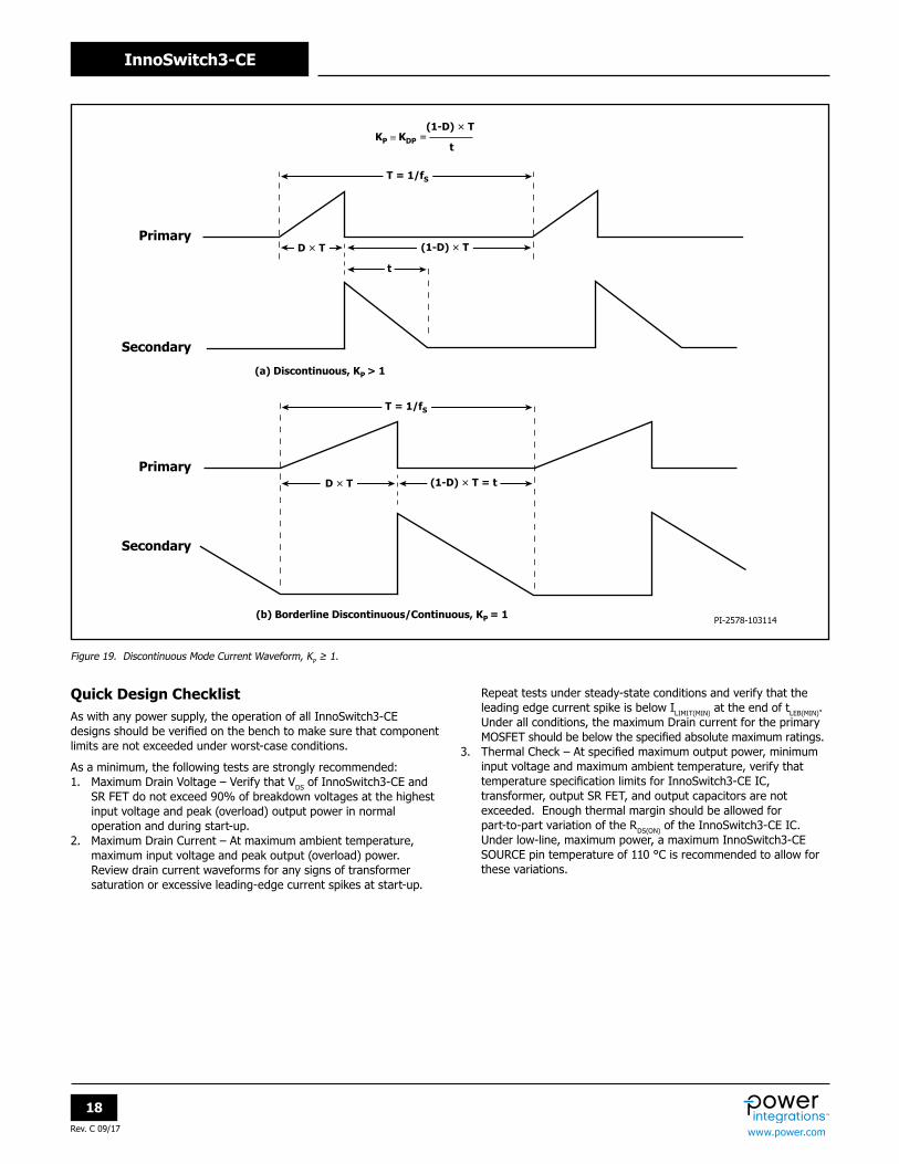
Ripple to Peak Current Ratio, KP A KP below 1 indicates continuous conduction mode, where KP is the ratio of ripple-current to peak-primary-current (Figure 18).
KP ≡ KRP = IR / IP
A value of KP higher than 1, indicates discontinuous conduction mode.In this case KP is the ratio of primary MOSFET off-time to the secondary diode conduction-time.
KP ≡ KDP = (1 – D) x T/ t = VOR × (1 – DMAX) / (VMIN – VDS) × DMAX
It is recommended that a KP close to 0.9 at the minimum expected DC bus voltage should be used for most InnoSwitch3-CE designs. A KP value of <1 results in higher transformer efficiency by lowering the primary RMS current but results in higher switching losses in the primary-side MOSFET resulting in higher InnoSwitch3-CE temperature. The benefits of quasi-resonant switching start to diminish for a further reduction of KP.
For a typical USB PD and rapid charge designs which require a wide output voltage range, KP will change significantly as the output voltage changes. KP will be high for high output voltage conditions and will drop as the output voltage is lowered. The PIXls spreadsheet can be used to effectively optimize selection of KP, inductance of the primary winding, transformer turns ratio, and the operating frequency while ensuring appropriate design margins.
Core TypeChoice of a suitable core is dependent on the physical limits of the power supply enclosure. It is recommended that only cores with low loss be used to reduce thermal challenges.
Safety Margin, M (mm)For designs that require safety isolation between primary and secondary that are not using triple insulated wire, the width of the safety margin to be used on each side of the bobbin is important. For universal input designs a total margin of 6.2 mm is typically required − 3.1 mm being used on either side of the winding. For vertical bobbins the margin may not be symmetrical. However if a total margin of 6.2 mm is required then the physical margin can be placed on only one side of the bobbin. For designs using triple insulated wire it may still be necessary to add a small margin in order to meet required creepage distances. Many bobbins exist for each core size and each will have different mechanical spacing. Refer to the bobbin data sheet or seek guidance to determine what specific margin is required. As the margin reduces the available area for the windings, the winding area will disproportionately reduce for small core sizes.
It is recommended that for compact power supply designs using an InnoSwitch3-CE IC, triple insulated wire should be used.
Primary Layers, LPrimary layers should be in the range of 1 < L < 3 and in general should be the lowest number that meets the primary current density limit (CMA). A value of ≥200 Cmils / Amp can be used as a starting point for most designs. Higher values may be required due to thermal constraints. Designs with more than 3 layers are possible but
Figure 18. Continuous Mode Current Waveform, KP ≤ 1.
the increased leakage inductance and the physical fit of the windings should be considered. A split primary construction may be helpful for designs where clamp dissipation due to leakage inductance is too high. In split primary construction, half of the primary winding is placed on either side of the secondary (and bias) winding in a sandwich arrangement. This arrangement is often disadvantageous for low power designs as this typically increases common mode noise and adds cost to the input filtering.
Maximum Operating Flux Density, BM (Gauss)A maximum value of 3800 Gauss at the peak device current limit (at 132 kHz) is recommended to limit the peak flux density at start-up and under output short-circuit conditions. Under these conditions the
output voltage is low and little reset of the transformer occurs during the MOSFET off-time. This allows the transformer flux density to staircase beyond the normal operating level. A value of 3800 Gauss at the peak current limit of the selected device together with the built-in protection features of InnoSwitch3-CE IC provide sufficient margin to prevent core saturation under start-up or output short-circuit conditions.
Transformer Primary Inductance, (LP)Once the lowest operating input voltage, switching frequency at full load, and required VOR are determined, the transformers primary inductance can be calculated. The PIXls design spreadsheet can be used to assist in designing the transformer.
Figure 19. Discontinuous Mode Current Waveform, KP ≥ 1.
Quick Design ChecklistAs with any power supply, the operation of all InnoSwitch3-CE designs should be verified on the bench to make sure that component limits are not exceeded under worst-case conditions.
As a minimum, the following tests are strongly recommended:1. Maximum Drain Voltage – Verify that VDS of InnoSwitch3-CE and
SR FET do not exceed 90% of breakdown voltages at the highest input voltage and peak (overload) output power in normal operation and during start-up.
2. Maximum Drain Current – At maximum ambient temperature, maximum input voltage and peak output (overload) power. Review drain current waveforms for any signs of transformer saturation or excessive leading-edge current spikes at start-up.
Repeat tests under steady-state conditions and verify that the leading edge current spike is below ILIMIT(MIN) at the end of tLEB(MIN). Under all conditions, the maximum Drain current for the primary MOSFET should be below the specified absolute maximum ratings.
3. Thermal Check – At specified maximum output power, minimum input voltage and maximum ambient temperature, verify that temperature specification limits for InnoSwitch3-CE IC, transformer, output SR FET, and output capacitors are not exceeded. Enough thermal margin should be allowed for part-to-part variation of the RDS(ON) of the InnoSwitch3-CE IC. Under low-line, maximum power, a maximum InnoSwitch3-CE SOURCE pin temperature of 110 °C is recommended to allow for these variations.
DRAIN Pin Voltage: .................................................. -0.3 V to 650 V DRAIN Pin Peak Current: INN3162C ........................ 880 mA (1.65 A)3
INN3163C .......................... 1.04 A (1.95 A)3
INN3164C .......................... 1.52 A (2.85 A)3
INN3165C .......................... 1.84 A (3.45 A)3
INN3166C .......................... 2.32 A (4.35 A)3
INN3167C .......................... 2.64 A (4.95 A)3
INN3168C .......................... 2.96 A (5.55 A)3
BPP/BPS Pin Voltage ........................................................-0.3 to 6 VBPP/BPS Current ................................................................. 100 mAFWD Pin Voltage ...................................................... -1.5 V to 150 VFB Pin Voltage .............................................................-0.3 V to 6 VSR Pin Voltage .............................................................-0.3 V to 6 VVOUT Pin Voltage .......................................................-0.3 V to 27 VV Pin Voltage ........................................................... -0.3 V to 650 VStorage Temperature ..................................................-65 to 150 °COperating Junction Temperature4 ................................ -40 to 150 °CAmbient Temperature .................................................-40 to 105 °CLead Temperature5 ............................................................... 260 °C
Notes:1. All voltages referenced to SOURCE and Secondary GROUND,
TA = 25 °C.2. Maximum ratings specified may be applied one at a time without
causing permanent damage to the product. Exposure to Absolute Maximum Ratings conditions for extended periods of time may affect product reliability.
3. Higher peak Drain current is allowed while the Drain voltage is simultaneously less than 400 V.
4. Normally limited by internal circuitry.5. 1/16” from case for 5 seconds.
Parameter Symbol
Conditions SOURCE = 0 V
TJ = -40 °C to 125 °C (Unless Otherwise Specified)
Min Typ Max Units
Control Functions
Startup Switching Frequency fSW TJ = 25 °C 23 25 27 kHz
Jitter Modulation Frequency fM TJ = 25 °C, fSW = 100 kHz 0.80 1.25 1.70 kHz
Maximum On-Time tON(MAX) TJ = 25 °C 12.4 14.6 16.9 ms
Notes:1. Soldered to 0.36 sq. inch (232 mm2) 2 oz. (610 g/m2) copper clad.2. Soldered to 1 sq. inch (645 mm2), 2 oz. (610 g/m2) copper clad.3. The case temperature is measured on the top of the package.
Parameter Conditions Rating Units
Ratings for UL1577
Primary-Side Current Rating Current from pin (16-19) to pin 24 1.5 A
Primary-Side Power Rating
TAMB = 25 °C (device mounted in socket resulting in TCASE = 120 °C) 1.35 W
• InnoSwitch3 Product Family • CE Series Number • Package Identifier
C InSOP-24D
• Features Code • Tape & Reel and Other Options
TL Tape & Reel, 2 k pcs per reel.INN 3162 C - H101 - TL
MSL Table
Part Number MSL Rating
INN3162C - INN3168C 3
ESD and Latch-Up Table
Test Conditions Results
Latch-up at 125 °C JESD78D > ±100 mA or > 1.5 × VMAX on all pins
Human Body Model ESD ANSI/ESDA/JEDEC JS-001-2014 > ±2000 V on all pins
Charge Device Model ESD ANSI/ESDA/JEDECJS-002-2014 > ±500 V on all pins
Part Ordering Table1,2
Feature Code CDC AR
ThresholdOTP Response
AR and OVL Response
Output Profile VOUT OVP
Secondary Fault Response
H101 0 mV 63% Hysteretic AR Fixed CC 120% AR
H102 300 mV 63% Hysteretic AR Fixed CC 120% AR
H103 250 mV 63% Hysteretic AR Fixed CC 120% AR
H104 270 mV 63% Hysteretic AR Fixed CC 120% AR
H105 240 mV 63% Hysteretic AR Fixed CC 120% AR
H107 380 mV OL Latch Off Latch Off Fixed CC 120% Latch Off
H109 0 mV 3.45 V Hysteretic AR Fixed CC 120% AR
H110 380 mV OL Latch Off AR Fixed CC 120% Latch Off
Common Feature Code
Part H101 H102 H103 H104 H105 H107 H109 H110
INN3162C-H1XX
INN3163C-H1XX
INN3164C-H1XX
INN3165C-H1XX
INN3166C-H1XX
INN3167C-H1XX
INN3168C-H1XX
1For the latest updates, please visit www.power.com InnoSwitch Family page to Build Your Own InnoSwitch.2To download the feature code data sheet addendum, please visit www.power.com.
For the latest updates, visit our website: www.power.comPower Integrations reserves the right to make changes to its products at any time to improve reliability or manufacturability. Power Integrations does not assume any liability arising from the use of any device or circuit described herein. POWER INTEGRATIONS MAKES NO WARRANTY HEREIN AND SPECIFICALLY DISCLAIMS ALL WARRANTIES INCLUDING, WITHOUT LIMITATION, THE IMPLIED WARRANTIES OF MERCHANTABILITY, FITNESS FOR A PARTICULAR PURPOSE, AND NON-INFRINGEMENT OF THIRD PARTY RIGHTS.
Patent InformationThe products and applications illustrated herein (including transformer construction and circuits external to the products) may be covered by one or more U.S. and foreign patents, or potentially by pending U.S. and foreign patent applications assigned to Power Integrations. A complete list of Power Integrations patents may be found at www.power.com. Power Integrations grants its customers a license under certain patent rights as set forth at http://www.power.com/ip.htm.
Life Support PolicyPOWER INTEGRATIONS PRODUCTS ARE NOT AUTHORIZED FOR USE AS CRITICAL COMPONENTS IN LIFE SUPPORT DEVICES OR SYSTEMS WITHOUT THE EXPRESS WRITTEN APPROVAL OF THE PRESIDENT OF POWER INTEGRATIONS. As used herein:
1. A Life support device or system is one which, (i) is intended for surgical implant into the body, or (ii) supports or sustains life, and (iii) whose failure to perform, when properly used in accordance with instructions for use, can be reasonably expected to result in significant injury or death to the user.
2. A critical component is any component of a life support device or system whose failure to perform can be reasonably expected to cause the failure of the life support device or system, or to affect its safety or effectiveness.