+ All Categories
Home > Documents > ISSCC 2011 / SESSION 9 / WIRELESS & mm-WAVE CONNECTIVITY /...

ISSCC 2011 / SESSION 9 / WIRELESS & mm-WAVE CONNECTIVITY /...

Date post: 08-Jul-2018
Category:
Upload: truonghuong
View: 216 times
Download: 0 times
Share this document with a friend
3
168 2011 IEEE International Solid-State Circuits Conference ISSCC 2011 / SESSION 9 / WIRELESS & mm-WAVE CONNECTIVITY / 9.5 9.5 An 87GHz QPSK Transceiver with Costas-Loop Carrier Recovery in 65nm CMOS Shih-Jou Huang, Yu-Ching Yeh, Huaide Wang, Pang-Ning Chen, Jri Lee National Taiwan University, Taipei, Taiwan Modern high-speed wireless data links such as 60GHz RF and point-to-point communications activate research on Gb/s transceivers for V-band (50 to 75GHz) and W-band (75 to 110GHz). Conventional approaches in SiGe or III-V compounds simply consume too much power and occupy too large area, in addition to the integration difficulty. In CMOS realizations, baseband processors and high-speed digitizers also increase design complexity and power consump- tion. This paper introduces a fully integrated CMOS QPSK transceiver with base- band-less carrier- and data-recovery circuitry, significantly reducing power con- sumption while achieving up to 3.5Gb/s data rate. The QPSK transmitter is shown in Fig. 9.5.1. Providing a prototype for the 81- to-86GHz band and 94GHz band, we set up the carrier at 87GHz. An integer-N frequency synthesizer provides 77.3GHz LO and 9.7GHz IF signals, forming an 8/9-1/9 up-convert architecture. It contains a VCO running at 77.3GHz, ÷8 and ÷16 circuits, a type-IV PFD, a V-to-I converter, and an on-chip 2nd-order loop fil- ter. The frequency arrangement is also applied to the RX, making no potential frequency offset between the two. A QPSK modulator generates 4 phases (0°, 90°, 180°, and 270°) of the 9.7GHz IF signal and sends them to the up-convert mixer, creating the 87GHz RF signal. A mm-Wave balun converts differential RF inputs into single-ended mode to drive the PA. With the input capacitance of M 1 and M 2 absorbed by the mixer’s resonance network, the balun achieves conver- sion loss of 1.4dB if the transformer coupling factor is 0.6. The PA’s output is fed into a matched microstrip line, which connects to the waveguide adapter. To perform coherent demodulation, the LO clock in the RX must be synchronized in phase and frequency. Unlike typical baseband approaches that require high- speed ADCs (several GS/s) and signal processors (>1GHz), we realize the carri- er recovery in the analog domain (i.e., Costas loop). As depicted in Fig. 9.5.2, the receiver is composed of an LNA, a down-convert mixer, an IF amplifier, a 77.3GHz clock source (VCO) and its ÷8 descendants (9.7GHz I/Q signals), and a phase detector (PD) and a frequency detector (FD) for carrier recovery. After LNA amplification, the incoming RF signal is downconverted into IF by the VCO’s clock. Assuming the signal at node A is given by V A (t) = D I (t)cos(ω IF t + Δφ) + D Q (t)sin(ω IF t + Δφ), where D I , D Q denote the embedded data, ω IF is the LO 2 frequency (=2π×9.7GHz), and Δφ is the phase error between IF and LO 2 . After mixing and limiting, the two outputs V D (t) and V E (t) become D I (t) and D Q (t), respectively, given that 45°<Δφ<45°. The V C (V B ) and V D (V E ) are further mixed together, creating the final output V F proportional to sin(Δφ). As a result, the (V/I) 1 ’s output I CP1 pres- ents a sinusoidal characteristic as shown in the upper-left corner of Fig. 9.5.2. Denoting pumping current as I P when Δφ = π/4, the PD [together with (V/I) 1 ] gain is given by 2I P . The approximately linear behavior in the vicinity of the ori- gin makes itself a linear PLL with two correlated phase-adjusting mechanisms, i.e., LO 1 loop and LO 2 loop. Upon lock, the two demodulated data are found in nodes D and E, as expected. In addition to phase alignment, the VCO frequency has to be corrected at power on. It is possible to form another loop and push the VCO frequency into the lock range by means of an external crystal. A much better way to do so is to extend the Costas loop one step further. As shown in Fig. 9.5.2, examining the cross- and auto-correlation of signals V B and V C twice gives rise to an output contain- ing the frequency error information. Denoting the frequency error between LO 2 and IF signals as Δω, we follow the same calculation procedure and obtain the signals in nodes G and H: V G (t) = A V cos(4Δωt) V H (t) = A V sin(4Δωt), where A V represents the swing magnitude designed in our CML blocks. These two signals are separated by 90°. Whether V G is leading or lagging V H depends on the polarity of Δω, which can be easily detected by sampling one signal with the other [1]. As a result, the two limiters sharpen the sinusoids as square functions, and send them to an edge-triggered flip-flop. The error polarity is therefore applied to (V/I) 2 , which provides pumping current I CP2 (=5I CP1 ) to adjust the VCO control voltage accordingly. Note that to minimize undesired dis- turbance on the control line, the FD loop must be disabled when the loop is locked. Observing that V G will stay low when Δω ≈ 0, we apply V K (V G after lim- iting) to (V/I) 2 to automatically shut it down when the frequency locking is achieved. Similar to that in [1], this automatic shut-off mechanism saves signif- icant power and area. The QPSK modulator is illustrated in Fig. 9.5.3(a). Here, a DMUX parallelizes the input data and a mapping logic rearranges the sequences. After retiming, the two outputs are created to control the IF 2-to-1 selector and the clock synthesization mixer, where the former picks the proper phase (0°, 90°) and the latter the polar- ity (180°, 270°). To achieve such a high frequency, the VCO and dividers involve mm-Wave techniques [Fig. 9.5.3(b)]. It incorporates a cross-coupled LC oscilla- tor with thick-oxide varactors, which is followed by two stages of tuned ampli- fiers (M 3 -M 5 ) as buffers. A direct injection-locked frequency divider is employed here as the 1st divider stage, where the injection signal is ac-coupled to the gate of the switch M 7 [2]. Simulation shows that its lock range is approximately equal to 4GHz when V b = 0.8V. The interconnection between chip and antenna is of great importance. As shown in Fig. 9.5.4(a), we realize the coplanar strip to waveguide by a transition fabri- cated on a single-layer dielectric substrate [3]. With the chip flipped onto the microstrip line, the RF signal is coupled through the substrate to the matching element, which is connected to the waveguide (entrance of horn) tightly. The measured insertion loss of the transition is depicted in Fig. 9.5.4(b), where the maximum loss from 81 to 86GHz is less than 5.3dB. Figure 9.5.4(c) illustrates a photo of the assembly. The LNA, PA, and RF mixer designs are based on our pre- vious work in 60 and 77GHz [2,4]. The 3-stage LNA achieves gain of 18.5dB, and the 5-stage PA 13dB gain and 6dBm P 1dB . The transmitter and receiver are fabricated in 65nm CMOS technology. The TX and RX consume 212mW and 166mW, respectively, from a 1.2V supply. Figure 9.5.5(a) shows the TX’s output spectrum under 650Mb/s QPSK modulation with bit length of 2 31 1, revealing a sinc function centered at the carrier frequency (87GHz). The TX presents a phase noise of 85.8dBc/Hz at 1MHz offset. The spectrum of the carrier recovered in the RX is also demonstrated in Fig. 9.5.5(b), which reveals a phase noise of 77.7dBc/Hz at 1MHz offset and 88dBc/Hz at 10MHz offset. Figure 9.5.6(a) shows the recovered (and demuxed) data in the RX. With D in = 2.5Gb/s, the recovered data jitter measures 34ps,rms and 200ps,pp, respectively. In this testing, both the TX and the RX are connected to 24dBi horn antennas, separated by 1 meter of distance. The BER as a function of data rate is also investigated. Figure 9.5.6(b) depicts the results for different data patterns. BER < 10 11 can be obtained for input of 3.5Gb/s 2 7 1 PRBS. Figure 9.5.7 shows the die micrograph, which occupies 1.32×1mm 2 . In estima- tion, the longest distance for D in = 2.5Gb/s is approximately equal to 2km given that 48dBi dish antennas are available. Note that a conventional TRX without car- rier recovery [5] suffers from synchronization difficulty and cannot operate inde- pendently. A table summarizing the performance of this work is also included in Fig. 9.5.7. Acknowledgment: The authors thank the TSMC University Shuttle Program for chip fabrication. References: [1] J. Lee et al., “A 75-GHz Phase-Locked Loop in 90-nm CMOS Technique,” IEEE J. Solid-State Circuits, vol. 43, pp. 1414-1426, June 2008. [2] Y. Li et al., “A Fully-Integrated 77GHz FMCW Radar System in 65nm CMOS,” ISSCC Dig. Tech. Papers, pp. 216-217, Feb. 2010. [3] H. Iizuka et al., “Millimeter-Wave Microstrip Line to Waveguide Transition Fabricated on a Single Layer Dielectric Substrate,” IEICE Tran. Commun., pp. 1169-1177, June 2002. [4] J. Lee et al., “A Low-Power Fully Integrated 60GHz Transceiver System with OOK Modulation and On-Board Antenna Assembly,” ISSCC Dig. Tech. Papers, pp. 316-317, Feb. 2009. [5] C. Marcu et al., “A 90 nm CMOS Low-Power 60 GHz Transceiver with Integrated Baseband Circuitry,” IEEE J. Solid-State Circuits, vol. 44, pp. 3434- 3447, Dec. 2009. 978-1-61284-302-5/11/$26.00 ©2011 IEEE
Transcript

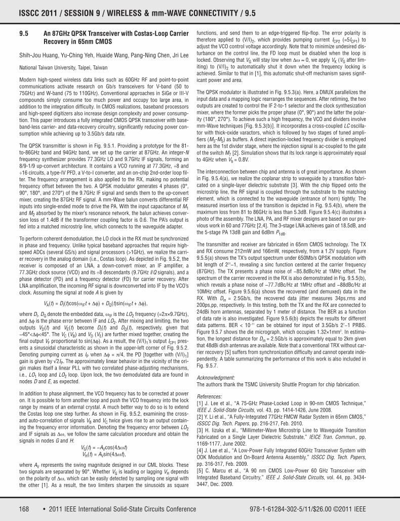
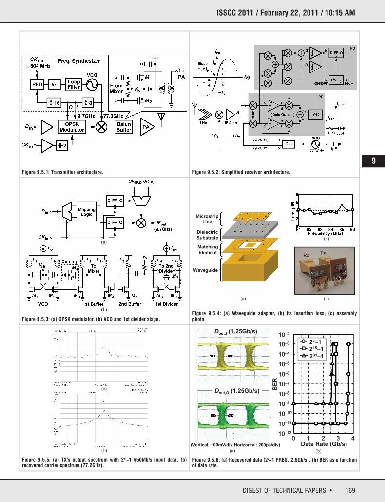
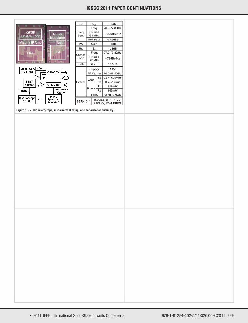
168 • 2011 IEEE International Solid-State Circuits Conference

ISSCC 2011 / SESSION 9 / WIRELESS & mm-WAVE CONNECTIVITY / 9.5

9.5 An 87GHz QPSK Transceiver with Costas-Loop Carrier Recovery in 65nm CMOS

Shih-Jou Huang, Yu-Ching Yeh, Huaide Wang, Pang-Ning Chen, Jri Lee

National Taiwan University, Taipei, Taiwan

Modern high-speed wireless data links such as 60GHz RF and point-to-pointcommunications activate research on Gb/s transceivers for V-band (50 to75GHz) and W-band (75 to 110GHz). Conventional approaches in SiGe or III-Vcompounds simply consume too much power and occupy too large area, inaddition to the integration difficulty. In CMOS realizations, baseband processorsand high-speed digitizers also increase design complexity and power consump-tion. This paper introduces a fully integrated CMOS QPSK transceiver with base-band-less carrier- and data-recovery circuitry, significantly reducing power con-sumption while achieving up to 3.5Gb/s data rate.

The QPSK transmitter is shown in Fig. 9.5.1. Providing a prototype for the 81-to-86GHz band and 94GHz band, we set up the carrier at 87GHz. An integer-Nfrequency synthesizer provides 77.3GHz LO and 9.7GHz IF signals, forming an8/9-1/9 up-convert architecture. It contains a VCO running at 77.3GHz, ÷8 and÷16 circuits, a type-IV PFD, a V-to-I converter, and an on-chip 2nd-order loop fil-ter. The frequency arrangement is also applied to the RX, making no potentialfrequency offset between the two. A QPSK modulator generates 4 phases (0°,90°, 180°, and 270°) of the 9.7GHz IF signal and sends them to the up-convertmixer, creating the 87GHz RF signal. A mm-Wave balun converts differential RFinputs into single-ended mode to drive the PA. With the input capacitance of M1and M2 absorbed by the mixer’s resonance network, the balun achieves conver-sion loss of 1.4dB if the transformer coupling factor is 0.6. The PA’s output isfed into a matched microstrip line, which connects to the waveguide adapter.

To perform coherent demodulation, the LO clock in the RX must be synchronizedin phase and frequency. Unlike typical baseband approaches that require high-speed ADCs (several GS/s) and signal processors (>1GHz), we realize the carri-er recovery in the analog domain (i.e., Costas loop). As depicted in Fig. 9.5.2, thereceiver is composed of an LNA, a down-convert mixer, an IF amplifier, a77.3GHz clock source (VCO) and its ÷8 descendants (9.7GHz I/Q signals), and aphase detector (PD) and a frequency detector (FD) for carrier recovery. AfterLNA amplification, the incoming RF signal is downconverted into IF by the VCO’sclock. Assuming the signal at node A is given by

VA(t) = DI(t)cos(ωIFt + Δφ) + DQ(t)sin(ωIFt + Δφ),

where DI, DQ denote the embedded data, ωIF is the LO2 frequency (=2π×9.7GHz),and Δφ is the phase error between IF and LO2. After mixing and limiting, the twooutputs VD(t) and VE(t) become DI(t) and DQ(t), respectively, given that−45°<Δφ<45°. The VC (VB) and VD (VE) are further mixed together, creating thefinal output VF proportional to sin(Δφ). As a result, the (V/I)1’s output ICP1 pres-ents a sinusoidal characteristic as shown in the upper-left corner of Fig. 9.5.2.Denoting pumping current as IP when Δφ = π/4, the PD [together with (V/I)1]gain is given by √2IP. The approximately linear behavior in the vicinity of the ori-gin makes itself a linear PLL with two correlated phase-adjusting mechanisms,i.e., LO1 loop and LO2 loop. Upon lock, the two demodulated data are found innodes D and E, as expected.

In addition to phase alignment, the VCO frequency has to be corrected at poweron. It is possible to form another loop and push the VCO frequency into the lockrange by means of an external crystal. A much better way to do so is to extendthe Costas loop one step further. As shown in Fig. 9.5.2, examining the cross-and auto-correlation of signals VB and VC twice gives rise to an output contain-ing the frequency error information. Denoting the frequency error between LO2and IF signals as Δω, we follow the same calculation procedure and obtain thesignals in nodes G and H:

VG(t) = −AVcos(4Δωt)VH(t) = AVsin(4Δωt),

where AV represents the swing magnitude designed in our CML blocks. Thesetwo signals are separated by 90°. Whether VG is leading or lagging VH dependson the polarity of Δω, which can be easily detected by sampling one signal withthe other [1]. As a result, the two limiters sharpen the sinusoids as square

functions, and send them to an edge-triggered flip-flop. The error polarity istherefore applied to (V/I)2, which provides pumping current ICP2 (=5ICP1) toadjust the VCO control voltage accordingly. Note that to minimize undesired dis-turbance on the control line, the FD loop must be disabled when the loop islocked. Observing that VG will stay low when Δω ≈ 0, we apply VK (VG after lim-iting) to (V/I)2 to automatically shut it down when the frequency locking isachieved. Similar to that in [1], this automatic shut-off mechanism saves signif-icant power and area.

The QPSK modulator is illustrated in Fig. 9.5.3(a). Here, a DMUX parallelizes theinput data and a mapping logic rearranges the sequences. After retiming, the twooutputs are created to control the IF 2-to-1 selector and the clock synthesizationmixer, where the former picks the proper phase (0°, 90°) and the latter the polar-ity (180°, 270°). To achieve such a high frequency, the VCO and dividers involvemm-Wave techniques [Fig. 9.5.3(b)]. It incorporates a cross-coupled LC oscilla-tor with thick-oxide varactors, which is followed by two stages of tuned ampli-fiers (M3-M5) as buffers. A direct injection-locked frequency divider is employedhere as the 1st divider stage, where the injection signal is ac-coupled to the gateof the switch M7 [2]. Simulation shows that its lock range is approximately equalto 4GHz when Vb = 0.8V.

The interconnection between chip and antenna is of great importance. As shownin Fig. 9.5.4(a), we realize the coplanar strip to waveguide by a transition fabri-cated on a single-layer dielectric substrate [3]. With the chip flipped onto themicrostrip line, the RF signal is coupled through the substrate to the matchingelement, which is connected to the waveguide (entrance of horn) tightly. Themeasured insertion loss of the transition is depicted in Fig. 9.5.4(b), where themaximum loss from 81 to 86GHz is less than 5.3dB. Figure 9.5.4(c) illustrates aphoto of the assembly. The LNA, PA, and RF mixer designs are based on our pre-vious work in 60 and 77GHz [2,4]. The 3-stage LNA achieves gain of 18.5dB, andthe 5-stage PA 13dB gain and 6dBm P1dB.

The transmitter and receiver are fabricated in 65nm CMOS technology. The TXand RX consume 212mW and 166mW, respectively, from a 1.2V supply. Figure9.5.5(a) shows the TX’s output spectrum under 650Mb/s QPSK modulation withbit length of 231−1, revealing a sinc function centered at the carrier frequency(87GHz). The TX presents a phase noise of −85.8dBc/Hz at 1MHz offset. Thespectrum of the carrier recovered in the RX is also demonstrated in Fig. 9.5.5(b),which reveals a phase noise of −77.7dBc/Hz at 1MHz offset and −88dBc/Hz at10MHz offset. Figure 9.5.6(a) shows the recovered (and demuxed) data in theRX. With Din = 2.5Gb/s, the recovered data jitter measures 34ps,rms and200ps,pp, respectively. In this testing, both the TX and the RX are connected to24dBi horn antennas, separated by 1 meter of distance. The BER as a functionof data rate is also investigated. Figure 9.5.6(b) depicts the results for differentdata patterns. BER < 10−11 can be obtained for input of 3.5Gb/s 27−1 PRBS.Figure 9.5.7 shows the die micrograph, which occupies 1.32×1mm2. In estima-tion, the longest distance for Din = 2.5Gb/s is approximately equal to 2km giventhat 48dBi dish antennas are available. Note that a conventional TRX without car-rier recovery [5] suffers from synchronization difficulty and cannot operate inde-pendently. A table summarizing the performance of this work is also included inFig. 9.5.7.

Acknowledgment:The authors thank the TSMC University Shuttle Program for chip fabrication.

References:[1] J. Lee et al., “A 75-GHz Phase-Locked Loop in 90-nm CMOS Technique,”IEEE J. Solid-State Circuits, vol. 43, pp. 1414-1426, June 2008.[2] Y. Li et al., “A Fully-Integrated 77GHz FMCW Radar System in 65nm CMOS,”ISSCC Dig. Tech. Papers, pp. 216-217, Feb. 2010.[3] H. Iizuka et al., “Millimeter-Wave Microstrip Line to Waveguide TransitionFabricated on a Single Layer Dielectric Substrate,” IEICE Tran. Commun., pp.1169-1177, June 2002.[4] J. Lee et al., “A Low-Power Fully Integrated 60GHz Transceiver System withOOK Modulation and On-Board Antenna Assembly,” ISSCC Dig. Tech. Papers,pp. 316-317, Feb. 2009.[5] C. Marcu et al., “A 90 nm CMOS Low-Power 60 GHz Transceiver withIntegrated Baseband Circuitry,” IEEE J. Solid-State Circuits, vol. 44, pp. 3434-3447, Dec. 2009.

978-1-61284-302-5/11/$26.00 ©2011 IEEE

169DIGEST OF TECHNICAL PAPERS •

ISSCC 2011 / February 22, 2011 / 10:15 AM

Figure 9.5.1: Transmitter architecture. Figure 9.5.2: Simplified receiver architecture.

Figure 9.5.3: (a) QPSK modulator, (b) VCO and 1st divider stage.

Figure 9.5.5: (a) TX’s output spectrum with 231−1 650Mb/s input data, (b)recovered carrier spectrum (77.2GHz).

Figure 9.5.6: (a) Recovered data (27−1 PRBS, 2.5Gb/s), (b) BER as a functionof data rate.

Figure 9.5.4: (a) Waveguide adapter, (b) its insertion loss, (c) assemblyphoto.

(a)

(b)

Waveguide

Matching

Element

Dielectric

Substrate

Microstrip

Line

(a)

(b)

(c)

TxRx

(a)

(b) (a)

Dout,I (1.25Gb/s)

Dout,Q (1.25Gb/s)

(Vertical: 100mV/div Horizontal: 200ps/div)

(b)

27 1215 1

231 1

Data Rate (Gb/s)

BE

R

9

• 2011 IEEE International Solid-State Circuits Conference 978-1-61284-302-5/11/$26.00 ©2011 IEEE

ISSCC 2011 PAPER CONTINUATIONS

Figure 9.5.7: Die micrograph, measurement setup, and performance summary.

PALNA

Mixer + IF Amp

QPSKCostas Loop

Balun

QPSKModulator

Overall

Supply 1.2V

RF Carrier 86.5-87.5GHz

AreaTx 0.57 0.95mm2

Rx 0.75 1mm2

PowerTx 212mW

Rx 166mW

Tech. 65nm CMOS

BER 10 11 3.5Gb/s, 27 1 PRBS2.8Gb/s, 215 1 PRBS

Rx S11 23dB

CostasLoop

Freq. 77.2-77.8GHzPNoise@1MHz

78dBc/Hz

LNA Gain 18.5dB

Tx S22 7dB

Freq.Syn.

Freq. 76.9-77.8GHzPNoise@1 MHz

85.8dBc/Hz

Ref. spur 42dBcPA Gain 13dB

x

x


Recommended