13
ITRS Emerging Logic Device working group George Bourianoff, Intel San Francisco, Ca July 10, 2011 April 10, 2011 2011 ERD Meeting Potsdam, Germany 1
| Date post: | 18-Dec-2015 |
| Category: |
Documents |
| Upload: | theodore-baldwin |
| View: | 217 times |
| Download: | 0 times |
ITRS Emerging Logic Device working group
George Bourianoff, IntelSan Francisco, Ca
July 10, 2011
April 10, 2011 2011 ERD Meeting Potsdam, Germany 1
Outline
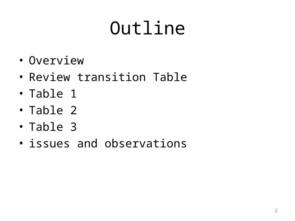
• Overview• Review transition Table• Table 1• Table 2• Table 3• issues and observations
2
Overview
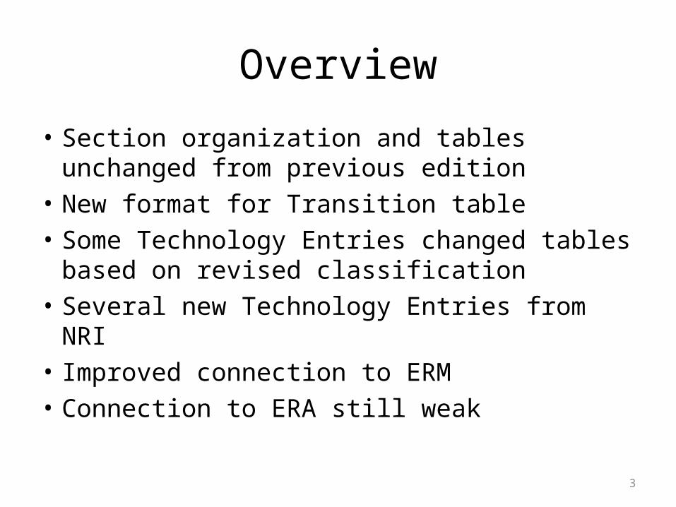
• Section organization and tables unchanged from previous edition
• New format for Transition table• Some Technology Entries changed tables
based on revised classification • Several new Technology Entries from NRI• Improved connection to ERM• Connection to ERA still weak
3

2011 Logic Transition Table
4
2009 2011 Comment
CNT FET CNT FET
GNR FET GNR FET
Nanowire FET Nanowire FET
Tunnel FET transferred from table 2
III-V FET Compound III-V chanel FETs partially transferred to PIDs
Ge FET Ge N channel MOSFET renamed
Unconventional Geormetries Transferred to PIDs
Spin FET/ Spin MOSFET Spin FET / Spin MOSFET
IMOS IMOS
MEMs MEMs
Atomic Switch New entry
Mot FET New entry
Ferroelectric FET transferred to table 3
Tunnel FET transferred to table 1
SET dropped - insufficient research activity
Collective Spin Devices Spin Wave Devices name change
Nano magnetic logic Nano matgnetic logic
Pseudospintronic BISFET name change
Molecular insufficient research activity
Excitonic FET new device concept
Atomic Switch transferred to table 2
Moving Domain Wall insufficient research activity
Ferroelectric Neg Cg Transferred and modified from table 2
Spin Torque Majority gate new device concept
All spin logic new device concept
Table 1
Table 2
Table 3
Table ERD6

Transition table discussion
• Adds clarity– Unchanged entries – no comment– Dropped entries – easy to indicate reason– New entries – show up clearly– Holding entries for possible future inclusion-
• easy to indicate • None in current table

2011 Table 1 MOSFETs Extending MOSFETs to the End of the roadmap
6
Table ERD7aMOSFETS: Extending MOSFETs to the End of the Roadmap.”
Cell Size Projected 100 nm 100 nm 100 nm 40 nm [M] 20 nm TBD(spatial pitch)
[B] Demonstrated 590 nm 1.4μm[G] 1.4μm[G]] 1 µ [N]sub 60
nm[A],60nm[B] 80nm = Lg x 2 [B] 60nm = Lg x 2 [A]
Projected 1.00E+10 1.00E+10 1.00E+10 5.9E+10 [M]channel down to 20nm
[C, D]: 1E10
Demonstrated 2.80E+08 5.10E+07 5.10E+07 5.2E+07 [M] not known1.5E+10 = 1/(4*Lg^2)
[B] 2.7E+10 = 1/(4*Lg^2) [A]
Projected 12 THz 7 THz [H] 7 THz [H] 6.5 THz [O]Si /InAs TFET: 60GHz/3THz [E]
Demonstrated 1.5 THz 300GHz [I] 300GHz [I] 250 GHz [P] not known 140GHz [B] 601GHz [A]
Projected 61 GHz not known not known 100 GHz [Q]Si/InAs TFET inverter:
20GHz, 1THz [E]
Demonstrated 5.6 GHz 22 kHz [J] 22 kHz [J] 11.7 MHz [R] not known Not Known TBD
Projected 3.00E-18 not known not known 4E-20 [S]CGG*VDD^2 (J/um)
< 2E-17 [F] 10-18
J TBD
Demonstrated 1.00E-16 not known not known 6.0E-16 [T]CGG*VDD^2 (J/um) =1E-
16 [F] N/A TBD
Projected 238 not known not known 5.90E+03 not known Not Known TBD
Demonstrated 1.6 not known not known 6.08E-04 not known Not Known TBD
TBD
TBD
Si, Ge, III-V, II-VI, TBD
In2O3, ZnO, TiO2, SiC TBD
330 not known Not Known TBD
All Si, Ge and silicide source, VLS
nanowire
N Ge FET
Device
FET [A]
Nanowire FETs
Circuit Speed
Binary Throughput,
GBit/ns/cm2
Switching Energy, J
Tunnel FET
Density
(device/cm2)
Ga(In)Sb
Switch Speed
Research Activity [AD]
N channel MOSFETS P channel MOSFETs
Typical example devices Si CMOS CNT FET Graphene Nanoribbon FET
Operational Temperature RT RT RT RT
Material Challenges Si
dialectrics, substrates, in situ mobility,
contactsCNT density,
contacts
RT
not known
RT
Low defect oxide interfaces

Table 1 discussion
• Si CMOS reference – which device?• Demonstrated CNTFET circuit speed increased from 220Hz to
56 MHz
• Demonstrated τs for GNRFET increased from 26 GHz to 300 GHz
• Significant progress on Ge/oxide interface to improve N channel mobility, short channel, N type Ge MOSFET elusive, lower resistance contacts needed
• Tunnel FETs: many demonstrations of SS< 60mV/ decade and Ion/Ioff >105. Low Ion remains problem

2001 Table II –Charge based beyond CMOS
Japan EU EU Japan US
bCell Size(spatial pitch) [B]
sub-1000nm [I2-I4]1.00E+10
Demonstrated 2.80E+08 Not known <1E7 >1E8 [M4] Not known~6.7E5
[1/(1um*150um)]
Limited by carrier mult. delay (CMD)
and stat. retard. delay (SRD) [I5-I6]
For IMOS with Lg=100nm,
Not knownCMD=0.6ns,
SRD=1.2ns [I6]
Similar to CMOS [I7]
limit by CMD &SRD
Not knownnot known
Similar to CMOS [I7]
Not knownnot known
Not known
Not known
Mott FET
Typical example devices Si CMOS Spin MOSFET Si, SiGe ([I1-I4]polySiGe/metal
[M1], CNT [M2], TiN [M3]
Atomic Switch MottFET
Device FET [A]Spin FET and Spin
MOSFETI MOS MEM Atomic Switch
10nm[1]
Not known
1umx150um [2]
Projected 100 nm 100nm [L] 100nm 100nm 40 nm
Demonstrated 590 nm Not known sub-1000nm Not known
~1E12 [1/(10nm*10nm)]
Switch Speed
Projected 12 THz 10 THz or less [N] ~1GHz [M5] Not known 2THz (0.5ps) [3]
Demonstrated 1.5 THz
Density
(device/cm 2 )
Projected 1.00E+10 1E10[L]>1.00E10 (due to
anchors)
0.18GHz [M6] ~ 2 ns13.3THz-0.1GHz(75fs-
9ns) [4]
Circuit SpeedProjected 61 GHz 10 GHz or less [N] ~1GHz [M5] Not known
Demonstrated 5.6 GHz 0.18MZ [M6] Not known
Table ERD7b Charge based Beyond CMOS: Non-Conventional FETs and other Charge-based information carrier devices
0.1uW [3]
Demonstrated 1.00E-16 Not known
Switching Energy, J
Projected 3.00E-18 ~1E-17 [N] <5E-17 [M7]
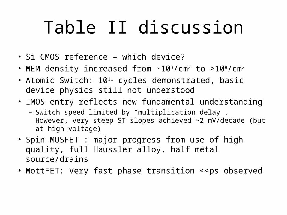
Table II discussion
• Si CMOS reference – which device?• MEM density increased from ~103/cm2 to >108/cm2
• Atomic Switch: 1011 cycles demonstrated, basic device physics still not understood
• IMOS entry reflects new fundamental understanding– Switch speed limited by “multiplication delay”. However, very
steep ST slopes achieved ~2 mV/decade (but at high voltage)
• Spin MOSFET : major progress from use of high quality, full Haussler alloy, half metal source/drains
• MottFET: Very fast phase transition <<ps observed
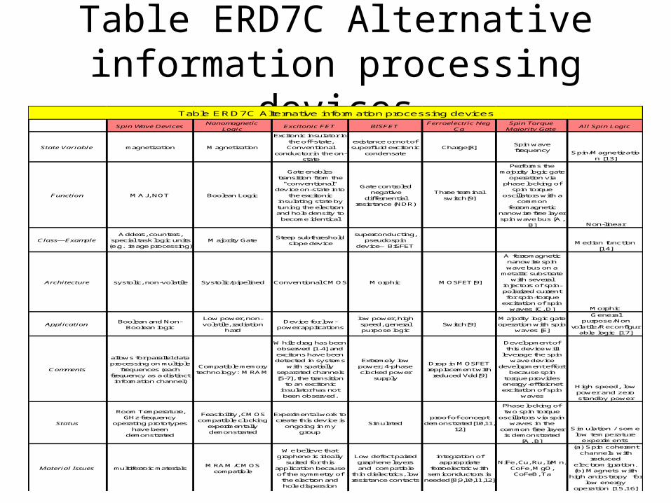
Table ERD7C Alternative information processing devices
Spin Wave DevicesNanomagnetic
LogicExcitonic FET BISFET
Ferroelectric Neg Cg
Spin Torque Majority Gate
All Spin Logic
State Variable magnetization Magnetization
Excitonic insulator in the off-state, Conventional
conductor in the on-state
existance or not of superfluid excitonic
condensateCharge[8]
Spin wave frequency Spin/Magnetizatio
n [13]
Function MAJ, NOT Boolean Logic
Gate enables transition from the
"conventional" device on-state into
the excitonic insulating state by tuning the electron and hole density to
become identical
Gate controled negative
differnential resistance (NDR)
Three terminal switch[9]
Performs the majority logic gate
operation via phase locking of
spin torque oscillators with a
common ferromagnetic
nanowire free layer spin wave bus [A,
B] Non-linear
Class—ExampleAdders, counters,
special task logic units (e.g. image processing)
Majority GateSteep subthreshold
slope device
superconducting, pseudospin
device—BiSFETMedian function
[14]
Architecture systolic, non-volatile Systolic/pipelined Conventional CMOS Morphic MOSFET[9]
A ferromagnetic nanowire spin wave bus on a
metallic substrate with several
injectors of spin-polarized current for spin-torque
excitation of spin waves [C, D] Morphic
ApplicationBoolean and Non-
Boolean logic
Low power, non-volatile, radiation
hard
Device for low-power applications
low power, high speed, general purpose logic
Switch[9]Majority logic gate operation with spin
waves [E]
General purpose/Non
volatile/Reconfigurable logic [17]
Comments
allows for parallel data processing on multiple
frequences (each frequency as a distinct information channel)
Compatible memory technology: MRAM
While drag has been observed [1-4] and excitons have been detected in systems
with spatially separated channels [5-7], the transition
to an excitonic insulator has not been observed.
Extremely low power; 4-phase clocked power
supply
Drop in MOSFET repplacement with
reduced Vdd[9]
Development of this device will
leverage the spin wave device
development effort because spin
torque provides energy-effieicnet excitation of spin
waves
High speed, low power and zero standby power
Status
Room Temperature, GHz frequency
operating prototypes have been
demonstrated
Feasibility, CMOS compatible clocking
experimentally demonstrated
Experimental work to create this device is
ongoing in my group
Simulatedproof of concept
demonstrated[10,11,12]
Phase locking of two spin torque
oscillators via spin waves in the
common free layer is demonstrated
[A, B]
Simulation / some low temperature
experiments
Material Issues multiferroic materialsMRAM/CMOS
compatible
We believe that graphene is ideally
suited for this application because of the symmetry of
the electron and hole dispersion
Low defect paired graphene layers and compatible
thin dielectrics, low resistance contacts
integration of appropriate
ferroelectric with semiconductors is
needed[8,9,10,11,12]
NiFe, Cu, Ru, IrMn, CoFe, MgO, CoFeB, Ta
(a) Spin coherent channels with
reduced electromigration. (b) Magnets with
high aniostropy for low energy
operation [15,16]
Table ERD7C Alternative information processing devices

Table III Discussion
• 4 new devices from NRI– Excitonic FET –ultra steep SS, room temperature operation problem– Spin Torque Majority Gate – 2 types, simulations only– All Spin Logic- simulations only
• NML: Clocking from fields generated by a metal line clad, ferromagnetic line, metastable magnetic configurations to reduce energy
• Ferroelectric negative Cg: Transferred from table 2 and modified: - SS <60mV/ decade demonstrated, single crystal ferroelectric oxide on Si an issue

Issues and observations
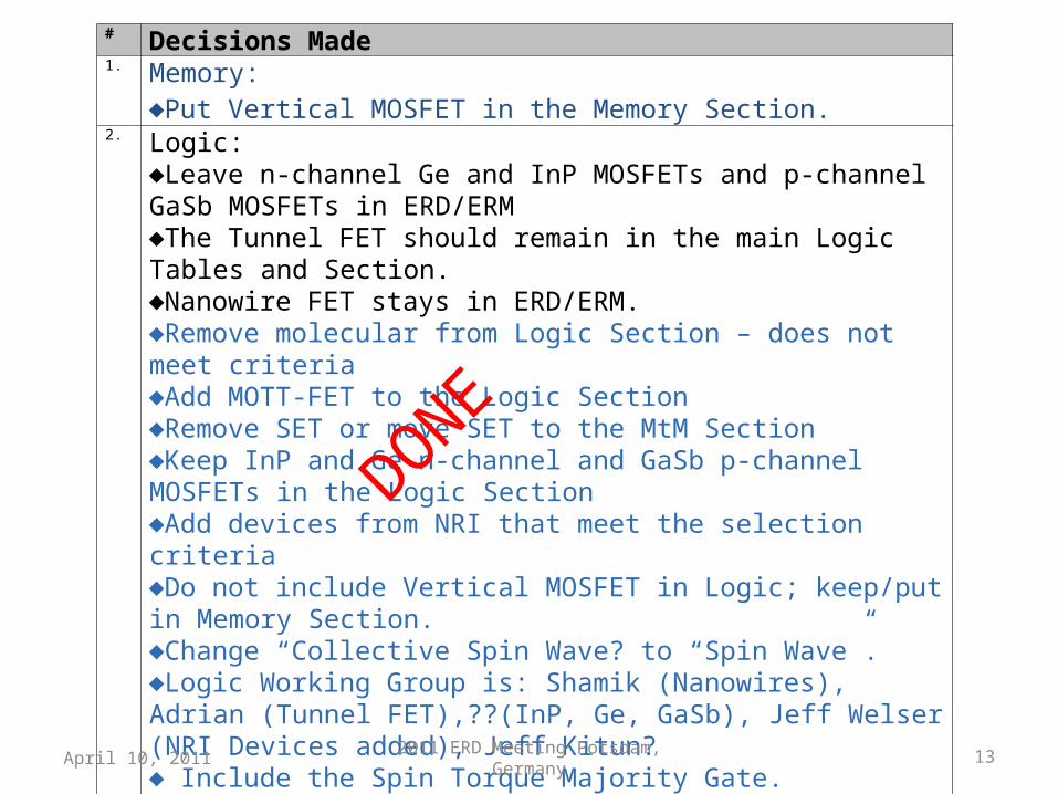
# Decisions Made1. Memory:
♦Put Vertical MOSFET in the Memory Section.2. Logic:
♦Leave n-channel Ge and InP MOSFETs and p-channel GaSb MOSFETs in ERD/ERM♦The Tunnel FET should remain in the main Logic Tables and Section.♦Nanowire FET stays in ERD/ERM.♦Remove molecular from Logic Section – does not meet criteria♦Add MOTT-FET to the Logic Section♦Remove SET or move SET to the MtM Section♦Keep InP and Ge n-channel and GaSb p-channel MOSFETs in the Logic Section♦Add devices from NRI that meet the selection criteria♦Do not include Vertical MOSFET in Logic; keep/put in Memory Section.♦Change “Collective Spin Wave? to “Spin Wave”.♦Logic Working Group is: Shamik (Nanowires), Adrian (Tunnel FET),??(InP, Ge, GaSb), Jeff Welser (NRI Devices added), Jeff Kitun? ♦ Include the Spin Torque Majority Gate.♦Keep the Atomic Switch in Logic Tables (corrected Feb. 17, 2011)
April 10, 2011 2011 ERD Meeting Potsdam, Germany 13
DONE


![ITRS Winter Conference 2007 Makuhara, Japan 1 International Technology Roadmap for Semiconductors 2007 ITRS ORTC [12/5 Makuhari Japan ITRS Public Conference]](https://static.documents.pub/doc/80x56/5514961d550346b0158b62f5/itrs-winter-conference-2007-makuhara-japan-1-international-technology-roadmap-for-semiconductors-2007-itrs-ortc-125-makuhari-japan-itrs-public-conference.jpg)


![International Technology Roadmap for Semiconductorsmaltiel-consulting.com/ITRS...Summary_2008_maltiel.pdf · 2008 ITRS Executive Summary Fig 5 [updated for 2007] Traditional . ORTC](https://static.documents.pub/doc/80x56/5f0ebd177e708231d440b30b/international-technology-roadmap-for-semiconductorsmaltiel-2008-itrs-executive.jpg)


