Lecture 20 Low Input Resistance Amplifiers (6/24/14) Page 20-1
CMOS Analog Circuit Design © P.E. Allen - 2016
LECTURE 20 – LOW INPUT RESISTANCE AMPLIFIERS – THE
COMMON GATE, CASCODE AND CURRENT AMPLIFIERS
LECTURE ORGANIZATION
Outline
• Voltage driven common gate amplifiers
• Voltage driven cascode amplifier
• Non-voltage driven cascode amplifier – the Miller effect
• Further considerations of cascode amplifiers
• Current amplifiers
• Summary
CMOS Analog Circuit Design, 3rd Edition Reference
Pages 218-236
Lecture 20 Low Input Resistance Amplifiers (6/24/14) Page 20-2
CMOS Analog Circuit Design © P.E. Allen - 2016
VOLTAGE-DRIVEN COMMON GATE AMPLIFIER
Common Gate Amplifier
Circuit:
Large Signal Characteristics:
VOUT(max) ≈ VDD – VDS3(sat)
VOUT(min) ≈ VDS1(sat) + VDS2(sat)
Note VDS1(sat) = VON1
060609-01
VDD
VPBias1
VNBias1
VNBias2
vOUTM3
M2
M1
VDD
vIN
vOUT
VNBias2
RL
IBias vIN
060609-02VON1
VT2
VON2
VON1+VON2
VDD VON3
vOUT
vINVNBias2
Lecture 20 Low Input Resistance Amplifiers (6/24/14) Page 20-3
CMOS Analog Circuit Design © P.E. Allen - 2016
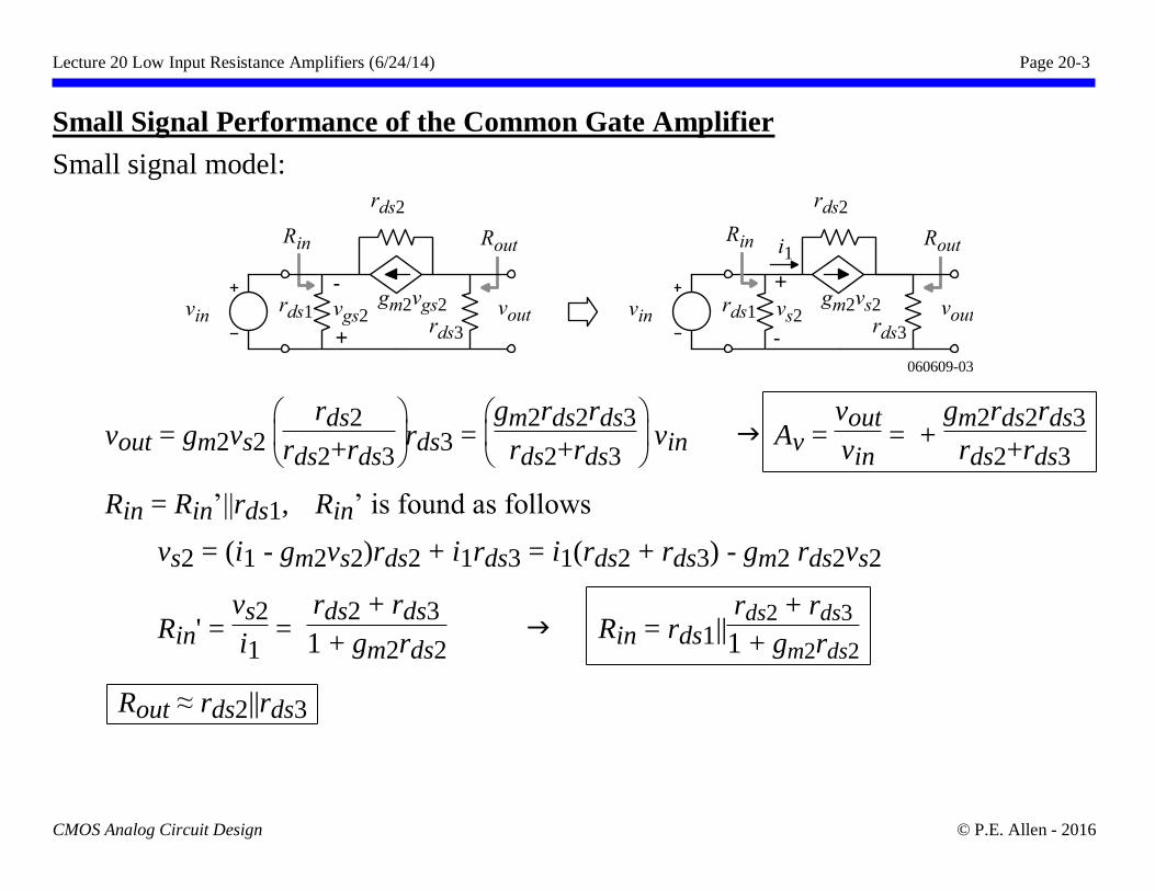
Small Signal Performance of the Common Gate Amplifier
Small signal model:
vout = gm2vs2
rds2
rds2+rds3rds3 =
gm2rds2rds3
rds2+rds3 vin Av =
vout
vin = +
gm2rds2rds3
rds2+rds3
Rin = Rin’||rds1, Rin’ is found as follows
vs2 = (i1 - gm2vs2)rds2 + i1rds3 = i1(rds2 + rds3) - gm2 rds2vs2
Rin' = vs2
i1 =
rds2 + rds3
1 + gm2rds2 Rin = rds1||
rds2 + rds3
1 + gm2rds2
Rout ≈ rds2||rds3
Rin
060609-03
gm2vgs2
+
-
vgs2
rds2
rds3
rds1vin vout
Rout
gm2vs2
+
-
vs2
rds2
rds3
rds1vin vout
RoutRin i1
Lecture 20 Low Input Resistance Amplifiers (6/24/14) Page 20-4
CMOS Analog Circuit Design © P.E. Allen - 2016
Influence of the Load on the Input Resistance of a Common Gate Amplifier
Consider a common gate amplifier with a general load:
From the previous page, the input resistance to the common gate configuration is,
Rin = rds2 + RLoad
1 + gm2rds2
For the various loads shown, Rin becomes:
Rin1 = rds2
1+gm2rds2 ≈
1
gm2 Rin2 =
rds2+rds3
1+ gm2rds2 ≈
2
gm2 Rin3 =
rds2+rds4gm3rds3
1+ gm2rds2 ≈ rds!!!
The input resistance of the common gate configuration depends on the load at the drain.
VDD
VNBias1
VNBias2
vOUT
M2
M1vIN
Load
VDD
VNBias1
VNBias2
vOUT
M2
M1vIN
VDD
VPBias1
VNBias1
VNBias2
vOUT
M3
M2
M1vIN
070420-01
VDDVPBias1
VNBias1
VNBias2
vOUTM3
M2
M1vIN
Rin1 Rin2
VPBias2
M4
Rin3
Lecture 20 Low Input Resistance Amplifiers (6/24/14) Page 20-5
CMOS Analog Circuit Design © P.E. Allen - 2016
VOLTAGE-DRIVEN CASCODE AMPLIFIER
Cascode† Amplifier
Advantages of the cascode amplifier:
• Increases the output resistance and gain (if M3 is cascoded also)
• Eliminates the Miller effect when the input source resistance is large
† “Cascode” = “Cascaded triode” see H. Wallman, A.B. Macnee, and C.P. Gadsden, “A Low-Noise Amplifier, Proc. IRE, vol. 36, pp. 700-708, June
1948.
060609-05
VDD
VPBias1
VNBias2
vOUTM3
M2
M1
vIN
Lecture 20 Low Input Resistance Amplifiers (6/24/14) Page 20-6
CMOS Analog Circuit Design © P.E. Allen - 2016
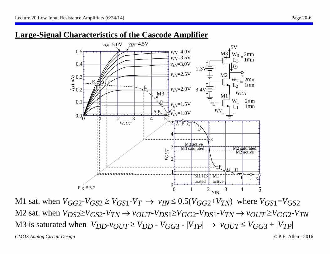
Large-Signal Characteristics of the Cascode Amplifier
M1 sat. when VGG2-VGS2 VGS1-VT → vIN 0.5(VGG2+VTN) where VGS1=VGS2
M2 sat. when VDS2VGS2-VTN → vOUT-VDS1VGG2-VDS1-VTN → vOUT VGG2-VTN
M3 is saturated when VDD-vOUT VDD - VGG3 - |VTP| → vOUT VGG3 + |VTP|
0 1 2 3 4 5
I D (
mA
)
vOUT
0 1 2 3 4 5
v OU
T
vIN
M2
M1
vIN
vOUT
ID
5V
+
-
+
-
W3L3
=2mm1mm
W1L1
=2mm1mm
Fig. 5.3-2
C
M3
2.3V
A B C
D
E
G H
I K
F
J
1
0
2
3
4
5
M3 saturated
EHI
K
J
M3 active
vIN=5.0V
vIN=4.0V
vIN=4.5V
vIN=1.0V
vIN=1.5V
vIN=2.0V
vIN=2.5V
0.0
0.1
0.2
0.3
0.4
0.5
vIN=3.5V
vIN=3.0V
D
A,B
G F
M2 activeM2 saturated
M1 sat-
urated
M1
active
3.4V
W2L2
=2mm1mm
M3
Lecture 20 Low Input Resistance Amplifiers (6/24/14) Page 20-7
CMOS Analog Circuit Design © P.E. Allen - 2016
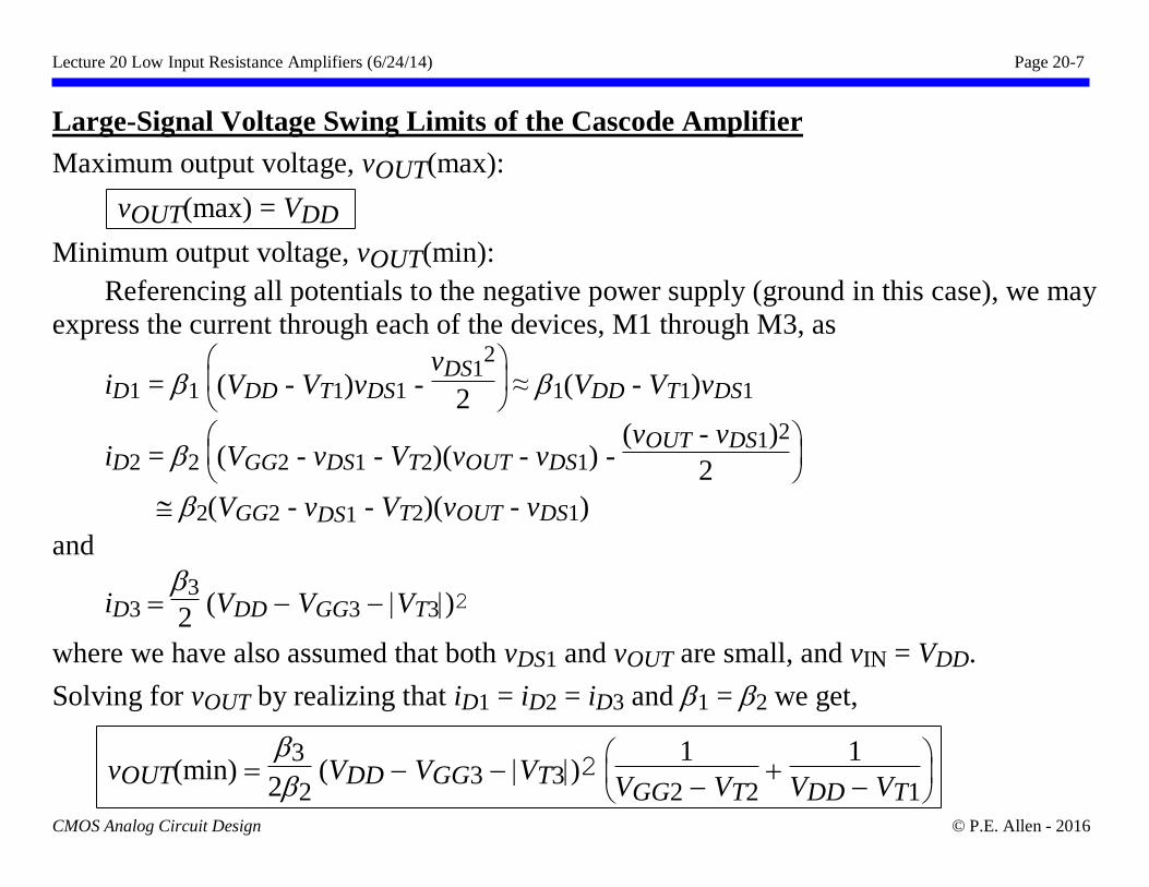
Large-Signal Voltage Swing Limits of the Cascode Amplifier
Maximum output voltage, vOUT(max):
vOUT(max) = VDD
Minimum output voltage, vOUT(min):
Referencing all potentials to the negative power supply (ground in this case), we may
express the current through each of the devices, M1 through M3, as
iD1 = 1
(VDD - VT1)vDS1 - vDS1
2
2 ≈ 1(VDD - VT1)vDS1
iD2 = 2
(VGG2 - vDS1 - VT2)(vOUT - vDS1) - (vOUT - vDS1)2
2
2(VGG2 - vDS1 - VT2)(vOUT - vDS1)
and
iD3 = 3
2 (VDD − VGG3 − VT3)2
where we have also assumed that both vDS1 and vOUT are small, and vIN = VDD.
Solving for vOUT by realizing that iD1 = iD2 = iD3 and 1 = 2 we get,
vOUT(min) = 3
22 (VDD − VGG3 − VT3)2
1
VGG2 − VT2 +
1
VDD − VT1
Lecture 20 Low Input Resistance Amplifiers (6/24/14) Page 20-8
CMOS Analog Circuit Design © P.E. Allen - 2016
Small-Signal Midband Performance of the Cascode Amplifier
Small-signal model:
Using nodal analysis, we can write,
[gds1 + gds2 + gm2]v1 − gds2vout = −gm1vin
−[gds2 + gm2]v1 + (gds2 + gds3)vout = 0
Solving for vout/vin yields
vout
vin =
−gm1(gds2 + gm2)
gds1gds2 + gds1gds3 + gds2gds3 + gds3gm2
−gm1
gds3 = −
2K'1W1
L1ID23
The small-signal output resistance is,
rout = [rds1 + rds2 + gm2rds1rds2]rds3 rds3
gm1vgs1 rds1
+
-
voutvin =vgs1
rds2
rds3
gm2vgs2= -gm2v1
+
-
Small-signal model of cascode amplifier neglecting the bulk ef fect on M2.
+
-
v1
G1 D1=S2 D2=D3
S1=G2=G3
gm1vin rds1
+
-
voutvin
rds2
rds3
+
-
+
-
v1
G1 D1=S2 D2=D3
1gm2
C2 gm2v1 C3
Simplified equivalent model of the above circuit. Fig. 5.3-3
C1
Lecture 20 Low Input Resistance Amplifiers (6/24/14) Page 20-9
CMOS Analog Circuit Design © P.E. Allen - 2016
Frequency Response of the Cascode Amplifier
Small-signal model (RS = 0):
where
C1 = Cgd1,
C2 = Cbd1+Cbs2+Cgs2, and
C3 = Cbd2+Cbd3+Cgd2+Cgd3+CL
The nodal equations now become:
(gm2 + gds1 + gds2 + sC1 + sC2)v1 − gds2vout = −(gm1 − sC1)vin
and −(gds2 + gm2)v1 + (gds2 + gds3 + sC3)vout = 0
Solving for Vout(s)/Vin(s) gives,
Vout(s)
Vin(s) =
1
1 + as + bs2
−(gm1 − sC1)(gds2 + gm2)
gds1gds2 + gds3(gm2 + gds1 + gds2)
where a = C3(gds1 + gds2 + gm2) + C2(gds2 + gds3) + C1(gds2 + gds3)
gds1gds2 + gds3(gm2 + gds1 + gds2)
and b = C3(C1 + C2)
gds1gds2 + gds3(gm2 + gds1 + gds2)
gm1vin rds1
+
-
voutvin
rds2
rds3
+
-
+
-
v1
G1 D1=S2 D2=D3
1gm2
C2 gm2v1 C3
Fig. 5.3-4A
C1
Lecture 20 Low Input Resistance Amplifiers (6/24/14) Page 20-10
CMOS Analog Circuit Design © P.E. Allen - 2016
A Simplified Method of Finding an Algebraic Expression for the Two Poles
Assume that a general second-order polynomial can be written as:
P(s) = 1 + as + bs2 =
1 − s
p1
1 − s
p2 = 1 − s
1
p1 +
1
p2 +
s2
p1p2
Now if p2 >> p1, then P(s) can be simplified as
P(s) ≈ 1 − s
p1 +
s2
p1p2
Therefore we may write p1 and p2 in terms of a and b as
p1 = −1
a and p2 =
−a
b
Applying this to the previous problem gives,
p1 = −[gds1gds2 + gds3(gm2 + gds1 + gds2)]
C3(gds1 + gds2 + gm2) + C2(gds2 + gds3) + C1(gds2 + gds3)
−gds3
C3
The nondominant root p2 is given as
p2 = −[C3(gds1 + gds2 + gm2) + C2(gds2 + gds3) + C1(gds2 + gds3)]
C3(C1 + C2)
−gm2
C1 + C2
Assuming C1, C2, and C3 are the same order of magnitude, and gm2 is greater than gds3,
then p1 is smaller than p2. Therefore the approximation of p2 >> p1 is valid.
Note that there is a right-half plane zero at z1 = gm1/C1.
Lecture 20 Low Input Resistance Amplifiers (6/24/14) Page 20-11
CMOS Analog Circuit Design © P.E. Allen - 2016
Repeating the Previous Example Using Intuitive Approach
Circuit:
Gain:
vout ≈ (-gm1vin) rds3 ⇒ vout
vin ≈ -gm1rds3
Poles:
1.) Dominant pole (one with the largest resistance to
ground):
p1 ≈ -1
rds3C3
2.) Next dominant pole is p2 ≈ -1
Rin(C1+C2)
However, in this case, p1 has already shorted the output to ground so that Rin is ≈ 1
gm2
rather than ≈ 2
gm2. Thus, p2 ≈
-gm2
C1+C2.
Much easier!!!
120515-01
VDD
VPBias1
VNBias2
voutM3
M2
M1
vIN
rout ≈ rds3
Rin
vin+
-
gm1vin
p1
p2
Lecture 20 Low Input Resistance Amplifiers (6/24/14) Page 20-12
CMOS Analog Circuit Design © P.E. Allen - 2016
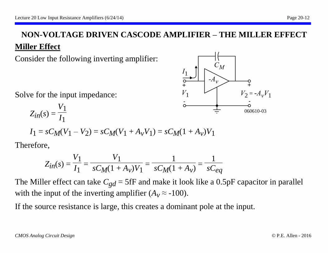
NON-VOLTAGE DRIVEN CASCODE AMPLIFIER – THE MILLER EFFECT
Miller Effect
Consider the following inverting amplifier:
Solve for the input impedance:
Zin(s) = V1
I1
I1 = sCM(V1 – V2) = sCM(V1 + AvV1) = sCM(1 + Av)V1
Therefore,
Zin(s) = V1
I1 =
V1
sCM(1 + Av)V1 =
1
sCM(1 + Av) =
1
sCeq
The Miller effect can take Cgd = 5fF and make it look like a 0.5pF capacitor in parallel
with the input of the inverting amplifier (Av ≈ -100).
If the source resistance is large, this creates a dominant pole at the input.
+
-
V1
I1-Av
+
-
V2 = -AvV1
CM
060610-03
Lecture 20 Low Input Resistance Amplifiers (6/24/14) Page 20-13
CMOS Analog Circuit Design © P.E. Allen - 2016
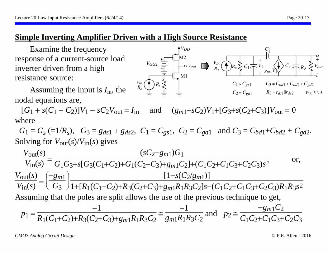
Simple Inverting Amplifier Driven with a High Source Resistance
Examine the frequency
response of a current-source load
inverter driven from a high
resistance source:
Assuming the input is Iin, the
nodal equations are,
[G1 + s(C1 + C2)]V1 − sC2Vout = Iin and (gm1−sC2)V1+[G3+s(C2+C3)]Vout = 0
where
G1 = Gs (=1/Rs), G3 = gds1 + gds2, C1 = Cgs1, C2 = Cgd1 and C3 = Cbd1+Cbd2 + Cgd2.
Solving for Vout(s)/Vin(s) gives
Vout(s)
Vin(s) =
(sC2−gm1)G1
G1G3+s[G3(C1+C2)+G1(C2+C3)+gm1C2]+(C1C2+C1C3+C2C3)s2 or,
Vout(s)
Vin(s) =
−gm1
G3
[1−s(C2/gm1)]
1+[R1(C1+C2)+R3(C2+C3)+gm1R1R3C2]s+(C1C2+C1C3+C2C3)R1R3s2
Assuming that the poles are split allows the use of the previous technique to get,
p1 = −1
R1(C1+C2)+R3(C2+C3)+gm1R1R3C2
−1
gm1R1R3C2 and p2
−gm1C2
C1C2+C1C3+C2C3
Lecture 20 Low Input Resistance Amplifiers (6/24/14) Page 20-14
CMOS Analog Circuit Design © P.E. Allen - 2016
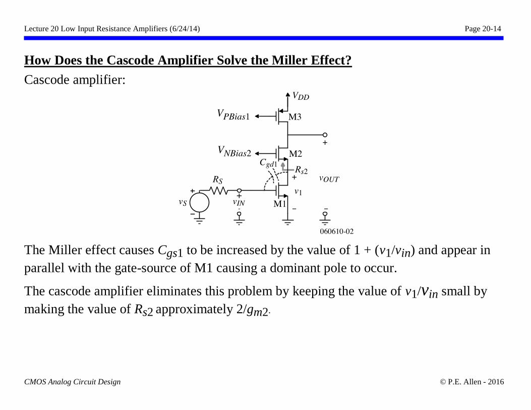
How Does the Cascode Amplifier Solve the Miller Effect?
Cascode amplifier:
The Miller effect causes Cgs1 to be increased by the value of 1 + (v1/vin) and appear in
parallel with the gate-source of M1 causing a dominant pole to occur.
The cascode amplifier eliminates this problem by keeping the value of v1/vin small by
making the value of Rs2 approximately 2/gm2.
Lecture 20 Low Input Resistance Amplifiers (6/24/14) Page 20-15
CMOS Analog Circuit Design © P.E. Allen - 2016
Comparison of the Inverting and Cascode Non-Voltage Driven Amplifiers
The dominant pole of the inverting amplifier with a large source resistance was found to
be
p1(inverter) = −1
R1(C1+C2)+R3(C2+C3)+gm1R1R3C2 ≈
−1
gm1R1R3C2
Now if a cascode amplifier is used, R3, can be approximated as 2/gm of the cascoding
transistor (assuming the drain sees an rds to ac ground).
p1(cascode) = −1
R1(C1+C2)+
2
gm(C2+C3)+gm1R1
2
gmC2
= −1
R1(C1+C2)+
2
gm(C2+C3)+2R1C2
−1
R1(C1+3C2)
Thus we see that p1(cascode) >> p1(inverter).
Lecture 20 Low Input Resistance Amplifiers (6/24/14) Page 20-16
CMOS Analog Circuit Design © P.E. Allen - 2016
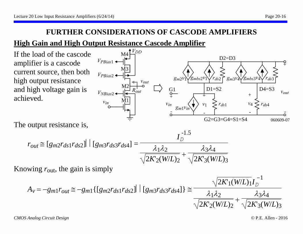
FURTHER CONSIDERATIONS OF CASCODE AMPLIFIERS
High Gain and High Output Resistance Cascode Amplifier
If the load of the cascode
amplifier is a cascode
current source, then both
high output resistance
and high voltage gain is
achieved.
The output resistance is,
rout [gm2rds1rds2][gm3rds3rds4] = I -1.5D
12
2K'2(W/L)2 +
34
2K'3(W/L)3
Knowing rout, the gain is simply
Av = −gm1rout −gm1{[gm2rds1rds2][gm3rds3rds4]} 2K'1(W/L)1I
-1D
12
2K'2(W/L)2 +
34
2K'3(W/L)3
060609-07
VDD
VPBias1
VPBias2
VNBias2
vin
vout
Rout
M3
M4
M2
M1
gm1vinrds1
gm2v1 gmbs2v1 rds2 gm3v4 gmbs3v4 rds3
rds4v1
+
-
v4
+
-
vout
+
-
G1 D1=S2 D4=S3
D2=D3
G2=G3=G4=S1=S4
vin
+
-
Lecture 20 Low Input Resistance Amplifiers (6/24/14) Page 20-17
CMOS Analog Circuit Design © P.E. Allen - 2016
Example 20-1 - Comparison of the Cascode Amplifier Performance
Calculate the small-signal voltage gain, output resistance, the dominant pole, and the
nondominant pole for the low-gain, cascode amplifier and the high-gain, cascode
amplifier. Assume that ID = 200 microamperes, that all W/L ratios are 2m/1µm, and
that the parameters of Table 3.1-2 are valid. The capacitors are assumed to be: Cgd = 3.5
fF, Cgs = 30 fF, Cbsn = Cbdn = 24 fF, Cbsp = Cbdp = 12 fF, and CL = 1 pF.
Solution
The low-gain, cascode amplifier has the following small-signal performance (no upper
cascode, just lower cascode):
Av = −37.1V/V Rout = 125k
p1 -gds3/C3 → 1.22 MHz p2 -gm2/(C1+C2) → 605 MHz.
The high-gain, cascode amplifier has the following small-signal performance (with upper
and lower cascode):
Av = −414V/V Rout = 1.40 M
p1 -1/RoutC3 → 108 kHz p2 -gm2/(C1+C2) → 579 MHz
(Note at this frequency, the drain of M2 is shorted to ground by the load capacitance, CL)
Lecture 20 Low Input Resistance Amplifiers (6/24/14) Page 20-18
CMOS Analog Circuit Design © P.E. Allen - 2016
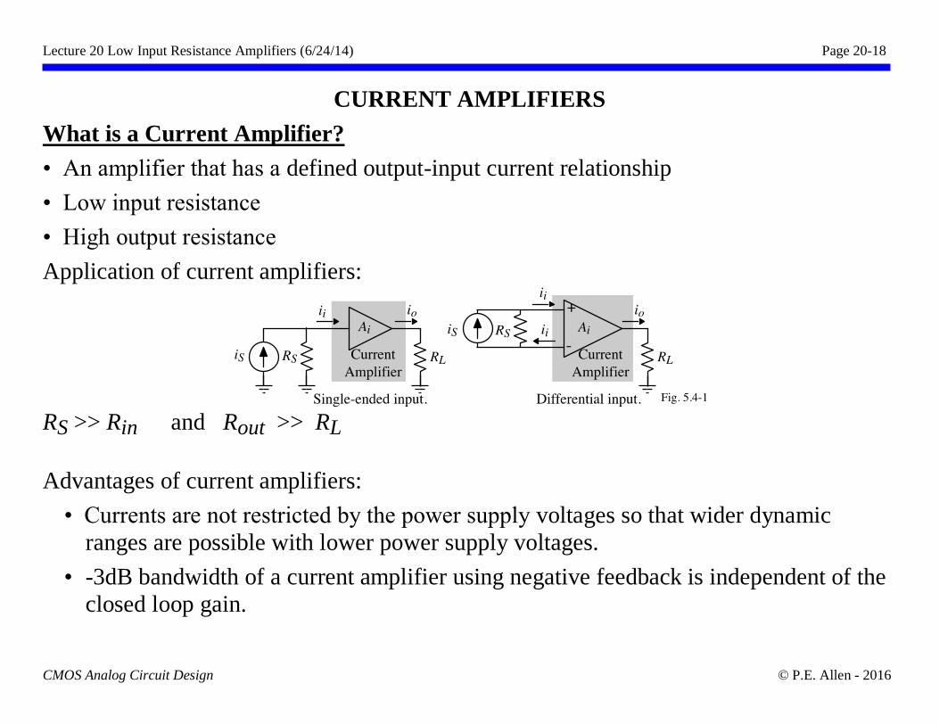
CURRENT AMPLIFIERS
What is a Current Amplifier?
• An amplifier that has a defined output-input current relationship
• Low input resistance
• High output resistance
Application of current amplifiers:
RS >> Rin and Rout >> RL
Advantages of current amplifiers:
• Currents are not restricted by the power supply voltages so that wider dynamic
ranges are possible with lower power supply voltages.
• -3dB bandwidth of a current amplifier using negative feedback is independent of the
closed loop gain.
Lecture 20 Low Input Resistance Amplifiers (6/24/14) Page 20-19
CMOS Analog Circuit Design © P.E. Allen - 2016
Frequency Response of a Current Amplifier with Current Feedback
Consider the following current amplifier with resistive
negative feedback applied.
Assuming that the small-signal resistance looking into
the current amplifier is much less than R1 or R2,
io = Ai(i1-i2) = Ai
vin
R1 - io
Solving for io gives
io =
Ai
1+Ai vin
R1 → vout = R2io =
R2
R1
Ai
1+Ai vin
If Ai(s) = Ao
s
A + 1
, then
vout
vin =
R2
R1
1
1+ 1
Ai(s)
= R2
R1
Ao
s
A +(1+Ao)
= R2
R1
Ao
1+Ao
1
s
A(1+Ao) +1
-3dB = A(1+Ao)
Lecture 20 Low Input Resistance Amplifiers (6/24/14) Page 20-20
CMOS Analog Circuit Design © P.E. Allen - 2016
Bandwidth Advantage of a Current Feedback Amplifier
The unity-gainbandwidth is,
GB = |Av(0)| -3dB = R2Ao
R1(1+Ao) · A(1+Ao) =
R2
R1 Ao·A =
R2
R1 GBi
where GBi is the unity-gainbandwidth of the current amplifier.
Note that if GBi is constant, then increasing R2/R1 (the voltage gain) increases GB.
Illustration:
Note that GB2 > GB1 > GBi
The above illustration assumes that the GB of the voltage amplifier realizing the voltage
buffer is greater than the GB achieved from the above method.
Ao dB
wA
R2
R1>1
R2
R1
GB1 GB2
Current Amplifier
0dB
Voltage Amplifier,
log10(w)
Magnitude dB
141013-01
(1+Ao)wA
GBi
= K
R1Voltage Amplifier, > K
R2
1+Ao
Ao dB
1+Ao
Ao dBK
Lecture 20 Low Input Resistance Amplifiers (6/24/14) Page 20-21
CMOS Analog Circuit Design © P.E. Allen - 2016
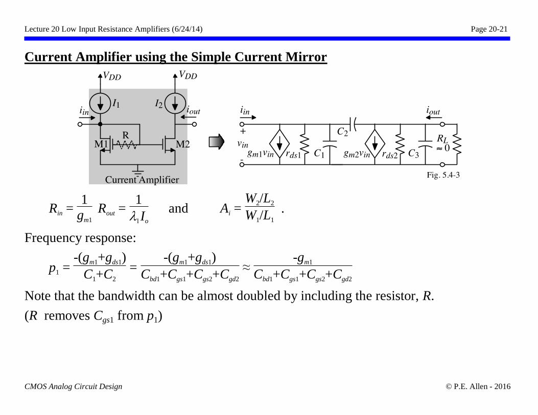
Current Amplifier using the Simple Current Mirror
Rin = 1
gm1
Rout = 1
Io
and Ai = W2/L2
W1/L1
.
Frequency response:
p1 = -(gm1+gds1)
C1+C2
= -(gm1+gds1)
Cbd1+Cgs1+Cgs2+Cgd2
≈ -gm1
Cbd1+Cgs1+Cgs2+Cgd2
Note that the bandwidth can be almost doubled by including the resistor, R.
(R removes Cgs1 from p1)
Lecture 20 Low Input Resistance Amplifiers (6/24/14) Page 20-22
CMOS Analog Circuit Design © P.E. Allen - 2016
Example 20-2 - Performance of a Simple Current Mirror as a Current Amplifier
Find the small-signal current gain, Ai, the input resistance, Rin, the output resistance,
Rout, and the -3dB frequency in Hertz for the current amplifier of previous slide if 10I1 =
I2 = 100µA and W2/L2 = 10W1/L1 = 10µm/1µm. Assume that Cbd1 = 10fF, Cgs1 = Cgs2 =
100fF, and Cgd2 = 50fF.
Solution
Ignoring channel modulation and mismatch effects, the small-signal current gain,
Ai = W2/L2
W1/L1 10A/A.
The small-signal input resistance, Rin, is approximately 1/gm1 and is
Rin 1
2KN(1/1)10µA =
1
46.9µS = 21.3k
The small-signal output resistance is equal to
Rout = 1
NI2 = 250k.
The -3dB frequency is
-3dB = 46.9µS
260fF = 180.4x10⁶ radians/sec. → f-3dB = 28.7 MHz
Lecture 20 Low Input Resistance Amplifiers (6/24/14) Page 20-23
CMOS Analog Circuit Design © P.E. Allen - 2016
Wide-Swing, Cascode Current Mirror Implementation of a Current Amplifier
Rin 1
gm1, Rout rds2gm4rds4, and Ai =
W2/L2
W1/L1
060610-01
+
M1 M2
M4
VDD
iout
vOUT
M3
-
+
-
IIN
VDD
IOUT
vIN
iin
VNBias2
Lecture 20 Low Input Resistance Amplifiers (6/24/14) Page 20-24
CMOS Analog Circuit Design © P.E. Allen - 2016
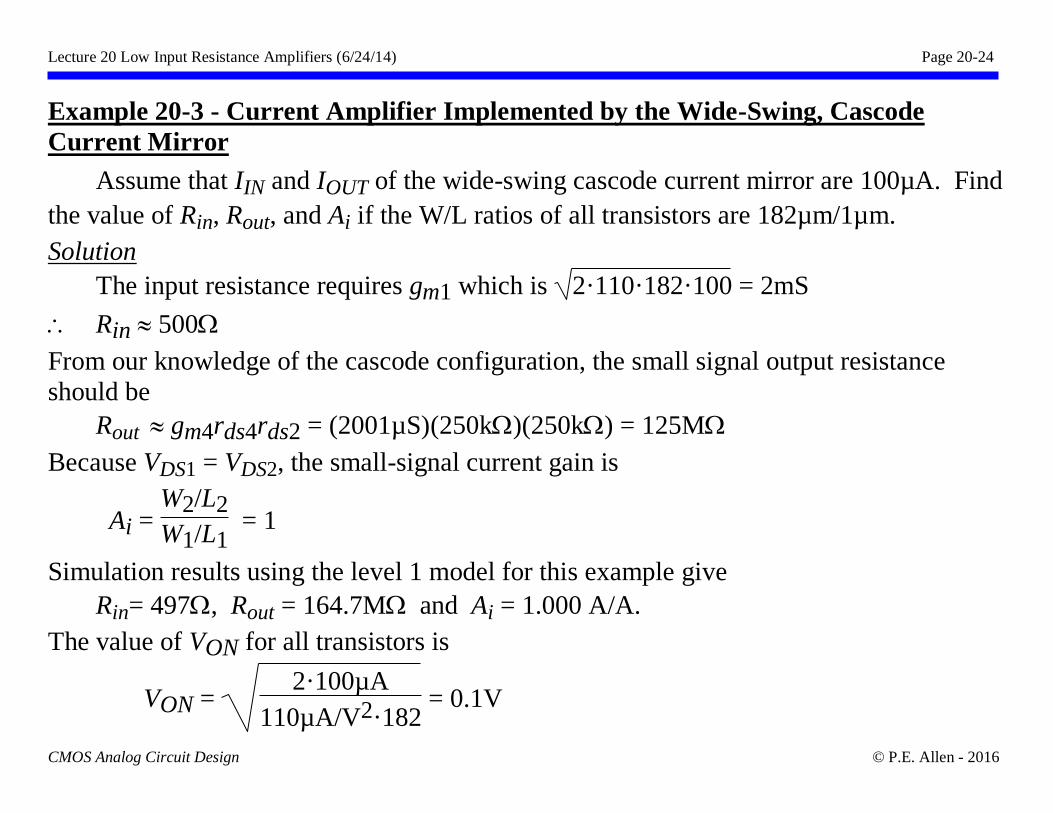
Example 20-3 - Current Amplifier Implemented by the Wide-Swing, Cascode
Current Mirror
Assume that IIN and IOUT of the wide-swing cascode current mirror are 100µA. Find
the value of Rin, Rout, and Ai if the W/L ratios of all transistors are 182µm/1µm.
Solution
The input resistance requires gm1 which is 2·110·182·100 = 2mS
Rin 500
From our knowledge of the cascode configuration, the small signal output resistance
should be
Rout gm4rds4rds2 = (2001µS)(250k)(250k) = 125M
Because VDS1 = VDS2, the small-signal current gain is
Ai = W2/L2
W1/L1 = 1
Simulation results using the level 1 model for this example give
Rin= 497, Rout = 164.7M and Ai = 1.000 A/A.
The value of VON for all transistors is
VON = 2·100µA
110µA/V2·182 = 0.1V
Lecture 20 Low Input Resistance Amplifiers (6/24/14) Page 20-25
CMOS Analog Circuit Design © P.E. Allen - 2016
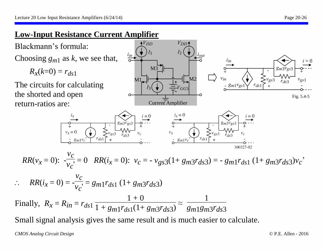
Low-Input Resistance Current Amplifier
To decrease Rin below 1/gm requires feedback but what kind of feedback?
Consider Blackman’s formulation for input resistance:
Rx = Rx(k=0)
1 + RR(port shorted)
1 + RR(port opened)
Therefore, we want a configuration where the return ratio (RR) goes to zero when the port
is shorted. We know that the shunt configuration shown below accomplishes this.
It is easy to see that the return ratio for the input shorted is zero and the return ratio for
the input open is,
RR(port opened) = Agm1rds1 ≠ 0
Therefore based on these ideas, a low-input resistance realization is proposed on the next
slide.
Lecture 20 Low Input Resistance Amplifiers (6/24/14) Page 20-26
CMOS Analog Circuit Design © P.E. Allen - 2016
Low-Input Resistance Current Amplifier
Blackmann’s formula:
Choosing gm1 as k, we see that,
Rx(k=0) = rds1
The circuits for calculating
the shorted and open
return-ratios are:
RR(vx = 0): -vc
vc' = 0 RR(ix = 0): vc = - vgs3(1+ gm3rds3) = - gm1rds1 (1+ gm3rds3)vc’
RR(ix = 0) = -vc
vc' = gm1rds1 (1+ gm3rds3)
Finally, Rx = Rin = rds1 1 + 0
1 + gm1rds1(1+ gm3rds3) ≈
1
gm1gm3rds3
Small signal analysis gives the same result and is much easier to calculate.
VGG3
M1
M3
M2
VDD VDD
I1 I2 ioutiin
I3
Current Amplifier
gm1vgs1 rds1rds3
gm3vgs3+
-
vgs1
+
-
vgs3
+
-
vin
iin
Fig. 5.4-5
i = 0
Lecture 20 Low Input Resistance Amplifiers (6/24/14) Page 20-27
CMOS Analog Circuit Design © P.E. Allen - 2016
Differential-Input, Current Amplifiers
Definitions for the differential-mode, iID, and common-mode, iIC, input currents of the
differential-input current amplifier.
iO = AIDiID ± AICiIC = AID(i1 - i2) ± AIC
i1+i2
2
Implementations:
I I2I
VDD VDD VDD
i1
i2 i2
iO
i1-i2M1 M2 M3 M4
iO
VDD
i1 i2M1 M2
M3 M4
M5 M6
VGG1
VGG2
Fig. 5.4-7
Lecture 20 Low Input Resistance Amplifiers (6/24/14) Page 20-28
CMOS Analog Circuit Design © P.E. Allen - 2016
SUMMARY
• Low input resistance amplifiers use the source as the input terminal with the gate
generally on ground
• The input resistance to the common gate amplifier depends on what is connected to the
drain
• The voltage driven common gate/common source amplifier has one dominant pole
• The current driven common gate/common source amplifier has two dominant poles
• The cascode amplifier eliminates the input dominant pole for the current driven
common gate/common source amplifier
• Current amplifiers have a low input resistance, high output resistance, and a defined
output-input current relationship
• Input resistances less than 1/gm require feedback
However, all feedback loops have internal poles that cause the benefits of negative
feedback to vanish at high frequencies.
In addition, feedback loops can have a slow time constant from a pole-zero pair.
• Voltage amplifiers using a current amplifier have high values of gain-bandwidth
• Current amplifiers are useful at low power supplies and for switched current
applications