SERBIAN JOURNAL OF ELECTRICAL ENGINEERING Vol. 11, No. 1, February 2014, 111-120 111 Linearization of Broadband Microwave Amplifier Aleksandra Đorić 1 , Nataša Maleš-Ilić 2 , Aleksandar Atanasković 2 , Bratislav Milovanović 2 Abstract: The linearization of broadband power amplifier for application in the frequency range 0.9–1.3 GHz is considered in this paper. The amplifier is designed for LDMOSFET characterized by the maximum output power 4W designing the broadband lumped element matching circuits and matching circuits in topologies that combines LC elements and transmission lines. The linearization of the amplifier is carried out by the second harmonics of the fundamental signals injected at the input and output of the amplifier transistor. The effects of linearization are considered for the case of two sinusoidal signals separated in frequency by different intervals up to 80 MHz ranging input power levels to saturation. Keywords: Amplifier, Linearization, Second harmonics, Intermodulation products. 1 Introduction Modern wireless comunication systems (CDMA-2000, WCDMA, OFDM etc.), are developing toward augmentation of frequency bandwidth to transmit a large number of carriers, with high velocity. In wireless comunication systems, Peak-to-Average Power Ratio (PAR) is very high, so that the power amplifiers (PA) in base stations need to satisfy the requirement of high linearity to amplify the signals with high PAR with a low distortion. The impact of the linearization tehnique that uses the second harmonics of fundamental signals (IM2) on the intermodulation products of narrowband power amplifiers has been analyzed in [1, 2] through the simulation process. The linearization was carried out by the simultaneous injection of the second harmonics to the input and output of the amplifier transistor. The experimental verification of the linearization method was performed on a standard narrowband amplifier at 1 GHz for two cases: when the linearization signals are led only at the output of the amplifier transistor and when linearization signals are simultaneously inserted at the input and output of the amplifier transistor [3]. 1 Innovation Centre of Advanced Technologies Niš, Vojvode Mišića 58, 18000 Niš, Serbia; E-mail: [email protected]2 Faculty of Electronic Engineering, University of Niš, Serbia, Aleksandra Medvedeva 14, 18000 Niš, Serbia; E-mails: [email protected]; [email protected]; [email protected]UDK: 621.396:004.72.057.4 DOI: 10.2298/SJEE131130010D
Transcript
SERBIAN JOURNAL OF ELECTRICAL ENGINEERING Vol. 11, No. 1, February 2014, 111-120
111
Linearization of Broadband Microwave Amplifier
Aleksandra Đorić1, Nataša Maleš-Ilić2, Aleksandar Atanasković2, Bratislav Milovanović2
Abstract: The linearization of broadband power amplifier for application in the frequency range 0.9–1.3 GHz is considered in this paper. The amplifier is designed for LDMOSFET characterized by the maximum output power 4W designing the broadband lumped element matching circuits and matching circuits in topologies that combines LC elements and transmission lines. The linearization of the amplifier is carried out by the second harmonics of the fundamental signals injected at the input and output of the amplifier transistor. The effects of linearization are considered for the case of two sinusoidal signals separated in frequency by different intervals up to 80 MHz ranging input power levels to saturation.
Keywords: Amplifier, Linearization, Second harmonics, Intermodulation products.
1 Introduction Modern wireless comunication systems (CDMA-2000, WCDMA, OFDM
etc.), are developing toward augmentation of frequency bandwidth to transmit a large number of carriers, with high velocity. In wireless comunication systems, Peak-to-Average Power Ratio (PAR) is very high, so that the power amplifiers (PA) in base stations need to satisfy the requirement of high linearity to amplify the signals with high PAR with a low distortion.
The impact of the linearization tehnique that uses the second harmonics of fundamental signals (IM2) on the intermodulation products of narrowband power amplifiers has been analyzed in [1, 2] through the simulation process. The linearization was carried out by the simultaneous injection of the second harmonics to the input and output of the amplifier transistor.
The experimental verification of the linearization method was performed on a standard narrowband amplifier at 1 GHz for two cases: when the linearization signals are led only at the output of the amplifier transistor and when linearization signals are simultaneously inserted at the input and output of the amplifier transistor [3]. 1Innovation Centre of Advanced Technologies Niš, Vojvode Mišića 58, 18000 Niš, Serbia; E-mail: [email protected]
A. Đorić, N. Maleš-Ilić, A. Atanasković, B. Milovanović
112
In this paper a broadband power amplifier is designed to operate over the frequency range 0.9–1.3 GHz and the linearization of the amplifier is carried out by simultaneous insertion of the second harmonics at the input and output of the amplifier transistor. The effects of the linearization are considered through the simulation for two sinusoidal signals with different frequency interval between them starting from 5 MHz and going up to 80 MHz, and for input signal power levels –5 dBm, 2 dBm and 10 dBm that is saturation level.
2 PA Design Approach Agilent Advanced Design System-ADS software package was used for
designing the broadband microwave amplifier. The amplifier was designed on the bases of the MET nonlinear model of Freescale transistor MRF281S LDMOSFET. The source and load impedances, (5.5 j15)sZ = + Ω and
(12.5 j27.5)lZ = + Ω , respectively, were obtained by source-pull and load-pull analysis in ADS. The satisfactory gain characteristic and matching at the input and output of the amplifier were attained over the frequency range 0.9–1.3 GHz. Detailed insight into the amplifier design process will be given in the following steps.
2.1 Matching circuit design In order to design a broadband amplifier circuit, the input and output
matching circuits of the transistor are based on the filter structures with lumped elements. Primarily, a lowpass prototype of filter with the order N = 3 was designed. The method of minimum reflection [4, 5] was used for calculating the normalized admittances of the prototype elements. The values of the reactive elements of the low-pass filter were calculated using the appropriate transformations [6]. Then, lowpass filter was transformed into a bandpass filter in a way that each series element was replaced by series resonant circuit, and each parallel element was replaced by a parallel resonant circuit at
0 1GHzω = [6].
Norton transformations [5] were applied in order to reduce values of some inductances and capacitances in the matching circuits, which did not correspond to the commercially available components. These transformations provide the scaling of the terminating resistors of matching circuits upwards or downwards to 50Ω using an ideal transformer with a certain transformation ratio n. After applying Norton transformations, approximately the same transmission characteristic and reflection losses were achieved in comparison with the basic matching circuit with lumped elements. Transformation ratio n = 1.2525 was selected for the input matching circuit, whereas n = 0.941 for the output matching circuit. Norton transformation implemented at the input matching circuit increases the terminating load from 31.87 Ω to 50 Ω, while at the output
Linearization of the Broadband Microwave Amplifier
113
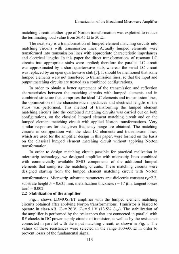
matching circuit another type of Norton transformation was exploited to reduce the terminating load value from 56.45 Ω to 50 Ω.
The next step is a transformation of lumped element matching circuits into matching circuits with transmission lines. Actually lumped elements were transformed into transmission lines with appropriate characteristic impedances and electrical lengths. In this paper the direct transformations of resonant LC circuits into appropriate stubs were applied; therefore the parallel LC circuit was approximated by a short quarterwave stub, whereas the serial LC circuit was replaced by an open quarterwave stub [7]. It should be mentioned that some lumped elements were not transfered to transmission lines, so that the input and output matching circuits are treated as a combined configurations.
In order to obtain a better agreement of the transmission and reflection characteristics between the matching circuits with lumped elements and in combined structure that comprises the ideal LC elements and transmission lines, the optimization of the characteristic impedances and electrical lengths of the stubs was performed. This method of transforming the lumped element matching circuits into the combined matching circuits was carried out on both configurations, on the classical lumped element matching circuit and on the lumped element matching circuit with applied Norton transformations. Very similar responses for the given frequency range are obtained. The matching circuits in configuration with the ideal LC elements and transmission lines, which are used for the amplifier design in this paper, were formed on the basis on the classical lumped element matching circuit without applying Norton transformation.
In order to design matching circuit possible for practical realization in microstrip technology, we designed amplifier with microstrip lines combined with commercially available SMD components of the additional lumped elements that comprise the matching circuits. These matching circuits were designed starting from the lumped element matching circuit with Norton transformations. Microstrip substrate parameters are: dielectric constant εr=2.2, substrate height h = 0.635 mm, metallization thickness t = 17 μm, tangent losses tan δ = 0.002. 2.2 Stabilization of the amplifier
Fig. 1 shows LDMOSFET amplifier with the lumped element matching circuits obtained after applying Norton transformations. Transistor is biased to operate in class-AB, VD = 26 V, VG = 5.1 V (13.5% IDSS). The stabilization of the amplifier is performed by the resistances that are connected in parallel with RF chocks in DC power supply circuits of transistor, as well as by the resistance connected in parallel with the input matching circuit, as shown in Fig. 1. The values of these resistances were selected in the range 300-600 Ω in order to prevent losses of the fundamental signal.
A. Đorić, N. Maleš-Ilić, A. Atanasković, B. Milovanović
114
Fig. 1 – Amplifier with the lumped element matching
circuits after applying Norton transformations.
Fig. 2 shows comparison of the S-parameters for three amplifier configurations, one with the lumped element matching circuits after applying Norton transformation (black dotted curve), the second with the combined ideal transmission line matching circuits and ideal lumped elements (grey curve) and the third relates to the microstrip matching circuit combined with the commercially available inductor and capacitor SMD components (black curve).
0.5 1.0 1.5 2.0 2.50.0 3.0
-20
-10
0
10
20
-30
30
freq, GHz
dB(S
(2,1
))(
(,
))
0.5 1.0 1.5 2.0 2.50.0 3.0
-10
-5
-15
0
freq, GHz
dB(S
(1,1
))(
())
a) b)
0.5 1.0 1.5 2.0 2.50.0 3.0
-8
-6
-4
-2
-10
0
freq, GHz
dB(S
(2,2
))(
())
c)
Fig. 2 – S-parameters of the amplifier with lumped element matching circuits after applying Norton transformations (black dotted curve),
combined ideal transmission line matching circuits (grey curve) and real combined microstrip matching circuit (black curve): (a) S21, (b) S11, (c) S22.
Linearization of the Broadband Microwave Amplifier
115
It can be noted from the Fig. 2 that the S11 and S22 parameters satisfy the requirements of appropriate matching at the input and output of transistor over the frequency band 0.9–1.3 GHz. For the amplifier with the combined ideal matching circuits a slightly worse matching is achieved at the amplifier output than for the lumped element matching circuits after applying Norton transformation. Additionally, the combined microstrip matching circuit provides better S11 parameters at the amplifier input, though the operational range is narrowed on the upper bandwidth side to approximately 1.25 GHz.
2.3 Linearization circuits With the aim to reduce the third-order intermodulation products of the
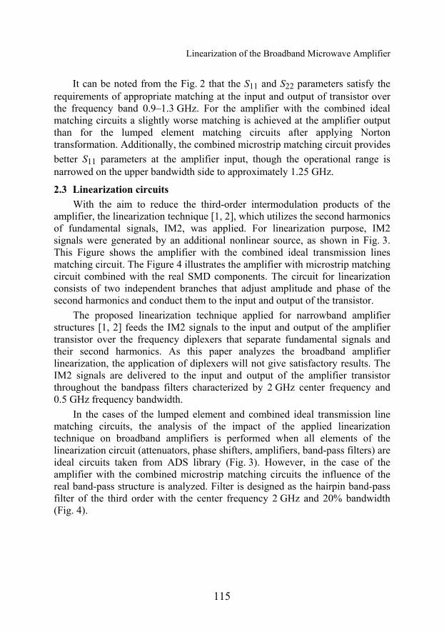
amplifier, the linearization technique [1, 2], which utilizes the second harmonics of fundamental signals, IM2, was applied. For linearization purpose, IM2 signals were generated by an additional nonlinear source, as shown in Fig. 3. This Figure shows the amplifier with the combined ideal transmission lines matching circuit. The Figure 4 illustrates the amplifier with microstrip matching circuit combined with the real SMD components. The circuit for linearization consists of two independent branches that adjust amplitude and phase of the second harmonics and conduct them to the input and output of the transistor.
The proposed linearization technique applied for narrowband amplifier structures [1, 2] feeds the IM2 signals to the input and output of the amplifier transistor over the frequency diplexers that separate fundamental signals and their second harmonics. As this paper analyzes the broadband amplifier linearization, the application of diplexers will not give satisfactory results. The IM2 signals are delivered to the input and output of the amplifier transistor throughout the bandpass filters characterized by 2 GHz center frequency and 0.5 GHz frequency bandwidth.
In the cases of the lumped element and combined ideal transmission line matching circuits, the analysis of the impact of the applied linearization technique on broadband amplifiers is performed when all elements of the linearization circuit (attenuators, phase shifters, amplifiers, band-pass filters) are ideal circuits taken from ADS library (Fig. 3). However, in the case of the amplifier with the combined microstrip matching circuits the influence of the real band-pass structure is analyzed. Filter is designed as the hairpin band-pass filter of the third order with the center frequency 2 GHz and 20% bandwidth (Fig. 4).
A. Đorić, N. Maleš-Ilić, A. Atanasković, B. Milovanović
116
Fig. 3 – Amplifier with combined ideal transmission line matching
network and additional circuit for linearization.
Fig. 4 – Amplifier with combined microstrip matching
network and additional circuit for linearization
3 Linearization of the Amplifier In order to assess the impact of the proposed linearization technique on the
designed broadband single-stage amplifier, two-tone test was performed in ADS. One sinusoidal signal at frequency 1 GHz and the other shifted in frequency by 5 MHz, 10 MHz, 20 MHz, 40 MHz or 80 MHz were simultane-ously driven at the amplifier input. At the amplifier output, power levels of the fundamental useful signals and power levels of their third order intermodulation products, IM3, were observed (IM3 - at frequency 1 22 f f− and IM3+ at frequency 2 12 f f− , if fundamental input signal frequencies are f1 and f2).
Linearization of the Broadband Microwave Amplifier
117
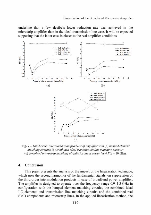
Fig. 5 to Fig. 7 show the power levels of the IM3 products before and after applying the linearization when input power levels of fundamental signals are -5dBm, 2dBm and 10dBm, respectively.
(a) (b)
(c)
Fig. 5 – Third-order intermodulation products of amplifier with (a) lumped element matching circuits; (b) combined ideal transmission line matching circuits; (c) combined
microstrip matching circuits for input power level Pin = –5 dBm.
It should be noted that, after the linearization, a significant reduction of the IM3 products was attained in a considered power range. However, the figures clearly indicate that the augmentation of the input signal power lessens the grade of IM3 reduction. In the case of 10 MHz interval between the signals, the IM3 are suppressed by 25 dB for the input power –5 dBm, whereas the rise of the input power to 10 dBm leads to 17 dB reduction of the IM3 products for the first and second case of the matching circuit topology. In the amplifier with lumped element matching circuits, for input power levels –5 dBm and 2 dBm, almost a uniform drop of the third-order intermodulation products was achieved for the various frequency intervals between the signals. However, the
A. Đorić, N. Maleš-Ilić, A. Atanasković, B. Milovanović
118
linearization grade of IM3 products falls from 20 dB in case of 10 MHz frequency interval to the value of 9 dB for 80 MHz interval when input power is 10 dBm.
(a) (b)
(c)
Fig. 6 – Third-order intermodulation products of amplifier with (a) lumped element matching circuits; (b) combined ideal transmission line matching circuits;
(c) combined microstrip matching circuits for input power level Pin = 2 dBm.
When frequencies of two tones are shifted by 40 MHz, the IM3 products decrease for approximately 20 dB at –5 dBm and 2 dBm input power and around 7dB for higher power levels in case of the combined ideal elements and transmission line matching circuit. Also, the linearization grade of IM3 is around 10 dB at –5 dBm and 2dBm input power and 6 dB in case of 10 dBm power when we consider 80 MHz frequency interval.
As far as the combined microstrip matching circuit amplifier is concerned by ranging the input power, the similar behavior of the linearization process is depicted in terms of the frequency interval between two tones in comparison with the combined ideal elements and transmission lines matching. We should indicate the asymmetry in power levels of IM3 products before linearization and
Linearization of the Broadband Microwave Amplifier
119
underline that a few decibels lower reduction rate was achieved in the microstrip amplifier than in the ideal transmission line case. It will be expected supposing that the latter case is closer to the real amplifier conditions.
(a) (b)
(c)
Fig. 7 – Third-order intermodulation products of amplifier with (a) lumped element matching circuits; (b) combined ideal transmission line matching circuits;
(c) combined microstrip matching circuits for input power level Pin = 10 dBm.
4 Conclusion This paper presents the analysis of the impact of the linearization technique,
which uses the second harmonics of the fundamental signals, on suppression of the third-order intermodulation products in case of broadband power amplifier. The amplifier is designed to operate over the frequency range 0.9–1.3 GHz in configuration with the lumped element matching circuits, the combined ideal LC elements and transmission line matching circuits and the combined real SMD components and microstrip lines. In the applied linearization method, the
A. Đorić, N. Maleš-Ilić, A. Atanasković, B. Milovanović
120
second harmonics are adjusted in amplitude and phase throughout two independent branches and inserted into the input and output of the amplifier transistor over the bandpass filter. Very good results in a reduction of the third-order nonlinearity of the amplifier are achieved for the considered three configurations of the amplifier matching circuits in case of the two-tone test. It is significant that the linearization of the third-order distortion is obtained in a range of signal power, all up to the point of saturation. Furthermore, the satisfactory results are gained even in cases when the frequency interval between signals rises to 80 MHz. However, it is noticeable that the intermodulation products decreasing grade descends when the power levels and interval between signals grow up.
5 Acknowledgement This work was supported by the Ministry of Education, Science and
Technological development of Republic of Serbia, the project number TR-32052.
6 References [1] N. Maleš-Ilić, B. Milovanović, Dj. Budimir: Improvement in Second Harmonics
Linearization Technique for Multichannel Amplifiers, Microwave and Optical Technology letters, Vol. 38, No. 2, July 2003, pp. 150 – 153.
[2] A. Atanasković, N. Maleš-Ilić, B. Milovanović: The Suppression of Intermodulation Products in Multichannel Amplifiers Close to Saturation, 11th WSEAS International Conference on Circuits, Agios Nikolaos, Crete Island, Greece, 23 – 25 July 2007, pp. 199 – 202.
[3] A. Atanasković, N. Maleš-Ilić, B. Milovanović: Linearization of Power Amplifiers by Second Harmonics and Fourth-order Nonlinear Signals, Microwave and Optical Technology Letters, Vol. 55, No. 2, Feb. 2013, pp. 425 – 430.
[4] G. Matthei, L. Young, E.M.T. Jones: Microwave Filters, Impedance-matching Networks and Coupling Structures, Artech House, Norwood, MA, USA, 1980.
[5] D.E. Dawson: Closed-form Solution for the Design of Optimum Matching Networks, IEEE Transaction on Microwave Theory and Techniques, Vol. 57, No. 1, Jan. 2009, pp. 121 – 129.
[6] B. Milovanović, V. Marković, N. Maleš-Ilić, O. Pronić-Rančić: Microwave Technology – Part I, Faculty of Electronic Engineering, University of Nis, Nis, Serbia, 2009. (In Serbian).
[7] R.W. Rhea: HF Filter Design and Computer Simulation, Noble, NY, USA, 1994.