Abstract: An extensive study of the single-step replication of form-birefringent quarter-wave plates is presented. Using rigorous diffractiontheory, the fabrication parameters and tolerances are carefully studiedin order to obtain ideal conditions for successful replication. The de-sign considerations are then applied to fabricate a master element byelectron-beam lithography, and to replicate quarter-wave plates using theUV-moulding process. The measurements show that the replicas behave ashigh-performance quarter-wave plates for the design wavelength.
References and links1. M. Born and E. Wolf, Principles of Optics, 7th ed. (Cambridge U. Press, Cambridge, UK, 1999).2. D. C. Flanders, “Submicrometer periodicity gratings as artificial anisotropic dielectrics,” Appl. Phys. Lett. 42,
492–494 (1983).3. R. C. Enger and S. K. Case, “Optical elements with ultrahigh spatial-frequency surface corrugations,” Appl. Opt.
22, 3220–3228 (1983).4. L. H. Cescato, E. Gluch, and N. Streibl, “Holographic quarter wave plates,” Appl. Opt. 29, 3286–3290 (1990).5. T. Isano, Y. Kaneda, N. Iwakami, K. Ishizuka, and N. Susuki, “Fabrication of half-wave plates with subwave-
length structures,” Jpn. J. Appl. Phys. 43, 5294–5296 (2004).6. F. Xu, R.-C. Tyan, P.-C. Sun, Y. Fainman, C.-C. Cheng, and A. Scherer, “Fabrication, modeling, and characteri-
zation of form-birefringent nanostructures,” Opt. Lett. 20, 2457–2459 (1995).7. D. L. Brundrett, E. N. Glytsis, and T. K. Gaylord, “Subwavelength transmission grating retarders for use at 10.6
microns,” Appl. Opt. 35, 6195–6202 (1996).8. L. Pang, M. Nezhad, U. Levy, C-H. Tsai, and Y. Fainman, “Form-birefringence structure fabrication in GaAs by
use of SU-8 as a dry-etching mask,” Appl. Opt. 44, 2377–2381 (2005).9. T. J. Kim, G. Campbell, and R. K. Kostuk, “Volume holographic phase retardation elements,” Opt. Lett. 20,
2030–2032 (1995).10. W. Yu, K. Satoh, H. Kikuta, T. Konishi, and T. Yotsuya, “Synthesis of wave plates using multilayered subwave-
length structure,” Jpn. J. Appl. Phys. 43, L439–L441 (2004).11. X. Deng, F. Liu, J. J. Wang, P. F. Sciortino, J. L. Chen and X. Liu, “Achromatic wave plates for optical pickup
units fabricated by use of imprint lithography,” Opt. Lett. 30, 2614–2616 (2005).12. J. J. Kim, X. Deng, X. Liu, A. Nikolov, P. Sciortino, F. Liu, and L. Chen, “Ultraviolet wave plates based on
monolithic integration of two fully filled and planarized nanograting layers,” Opt. Lett. 31, 1893–1895 (2006).13. T. Yoshikawa, T. Konishi, M. Nakajima, H. Kikuta, H.Kawata and Y. Hirai, “Fabrication of 1/4 wave plate by
nanocasting lithography,” J. Vac. Sci. Technol. B 23, 2939–2943 (2005).
#98476 - $15.00 USD Received 7 Jul 2008; revised 3 Sep 2008; accepted 4 Sep 2008; published 29 Sep 2008
(C) 2008 OSA 13 October 2008 / Vol. 16, No. 21 / OPTICS EXPRESS 16334
14. J. Pietarinen, V. Kalima, T. T. Pakkanen, and M. Kuittinen, “Improvement of UV-moulding accuracy by heat andsolvent assisted process,” Microelec. Eng. 85, 263–270 (2008).
15. N. Passilly, K. Ventola, P. Karvinen, P. Laakkonen,J. Turunen, and J. Tervo, “Polarization conversion in conicaldiffraction by metallic and dielectric subwavelength gratings,” Appl. Opt. 46, 4258–4265 (2007).
16. J. Turunen, M. Kuittinen, and F. Wyrowski, “Diffractive optics: electromagnetic approach,” Progr. Opt. 40, E.Wolf, ed. (Elsevier, Amsterdam, 2000), pp. 341–387.
17. L. Li, “A Modal Analysis of Lamellar Diffraction Gratings in Conical Mountings,” J. Mod. Opt. 40, 553–573(1993).
18. L. Li, “Use of Fourier series in the analysis of discontinuous periodic structures,” J. Opt. Soc. Am. A 13, 1870–1876 (1996).
19. L. Li, “Note on the S-matrix propagation algorithm,” J. Opt. Soc. Am. A 20, 655–660 (2003).20. M. T. Gale, “Replication,” in Micro-optics, elements, systems and applications, H. P. Herzig, ed., (Taylor &
Francis, London, 1997), pp. 153–178.21. T. Bailey, B.L. Choi, M. Colburn, M. Meissi, S. Shaya, J.G. Ekerdt, S.V. Sreenivasan, and C.G. Willson, “Step
and flash imprint lithography: Template surface treatment and defect analysis,” J. Vac. Sci. Technol. B 18, 3572–3577 (2000).
22. T. Levola and P. Laakkonen, “Replicated slanted gratings with a high refractive index material for in and outcou-pling of light,” Opt. Express 15, 2067–2074 (2007).
23. A. Amagai, M. Shimuta, M. Takeuchi and K. Mizuno, “Resin for optical material,” US patent 6117923 (2000).24. The Jones matrices appearing in Eq. (1) are given, e.g., in D. S. Kliger, J. W. Lewis, and C. E. Randall, Polarized
Light in Optics and Spectroscopy (Academic Press, San Diego, CA, 1990), Appendix B.
1. Introduction
Elements that provide phase retardation are key components in a number of different opti-cal systems. These phase retarders are usually made of materials that exhibit natural birefrin-gence. However, it has been shown during the last few decades, that Subwavelength PeriodGratings (SPGs) can also act as birefringent elements. In such a case, the period must be suf-ficiently small such that all diffracted orders, except for the zeroth, are evanescent. Thus, one-dimensional SPGs can be understood as artificial negative uniaxial materials whose optical axesare parallel to the grating vector [1]. The phenomenon is widely known as form birefringence.This artificial birefringence can be much larger than the natural one and hence the elements canbe as thin as several hundreds of nanometers, making them suitable for integration.
The first investigations of form-birefringent dielectric gratings for phase retardation werecarried out in the 1980’s. Flanders [2] measured the phase retardation produced by binary sil-icon nitride gratings, while Enger et al. [3] and, some years later, Cescato et al. [4] fabricatedgratings in SiO2 and in photoresist, respectively. Thanks to the high refractive index of siliconnitride, it was possible for Flanders [2] to achieve large retardation. However, the birefringenceof gratings made in lower refractive index materials [3, 4] was small and, consequently, bothEnger et al. and Cescato et al. proposed to fabricate elements whose retardation is equal to λ/8and to cascade them. Thus, although the form birefringence can be much larger than the nat-ural birefringence, use of high refractive indices is usually required if one desires to fabricatequarter-wave-plate-like or half-wave-plate-like elements [5] for visible wavelengths. When therefractive index is small, required aspect ratios (thickness-to-linewidth ratio) are high, leadingto extremely challenging fabrication. In addition to visible light, grating-based retarders havebeen designed and tested also for infra-red frequencies, for which semiconductor materials withhigh refractive indices, such as GaAs, can be used. In the infra-red range, the required minimumfeatures of the elements are larger and the aspect ratios are smaller, and hence the fabricationprocess is, in general, easier than in the visible wavelengths [6–8]. Another approach [9] is toemploy dichromated gelatin emulsion in order to holographically record a deep (the birefrin-gence of the emulsion being low) volume grating acting as a quarter wave plate (QWP).
It is obvious from the above-made discussion that, even if these elements have been exten-sively investigated, it is still very challenging to produce them easily in large quantities (becauseof required high-index material) and, consequently, at low cost. Yu et al. [10] investigated a
#98476 - $15.00 USD Received 7 Jul 2008; revised 3 Sep 2008; accepted 4 Sep 2008; published 29 Sep 2008
(C) 2008 OSA 13 October 2008 / Vol. 16, No. 21 / OPTICS EXPRESS 16335
multilayered element made by coating of a thin, high-index ZTO film onto a subwavelengthstructure fabricated on a low-index substrate that can be produced by replication techniques.However, weak directionality of film growth by sputtering can lead to a lack of accuracy in theretardation and the process still needs several steps. Nano-imprint lithography (usually alongwith Cr evaporation) can also be used to fabricate a mask before reactive ion etching [11, 12].Nevertheless, in order to further reduce the costs, faster techniques involving fewer steps are ab-solutely required. Some potential techniques leading to low-cost fabrication are hot-embossing,injection moulding, and UV-moulding. However, most of them are limited to relatively small as-pect ratios. Lately, methods to improve the ability of nanocasting lithography and UV-mouldingin high-aspect-ratio replication have been proposed [13, 14]. These methods involve heat andsolvent assisted processes or vacuum baking. Yoshikawa et al. [13] attempted to replicate, bynanocasting lithography, a quarter wave plate to polycarbonate from a quartz mold. The use ofPC (n∼ 1.55) compels to replicate high aspect ratio structure (period 400 nm, height 1900 nm)which can generate errors. For instance, the replicated element was actually 1/5 wave retarder(75◦ phase shift) instead of the targeted quarter-wave plate.
Recently, new UV-molding materials with high refractive index (n ∼ 1.7) have been devel-oped. In this paper, we intend to show that they are suitable for low-cost replication of highaspect-ratio structures and in particular of form-birefringent quarter wave plates. Conditions tofacilitate the replication are taken into account in the design. The paper is organized as follows:In Section 2, the design and the different requirements are considered, fabrication of the masterand replication is presented in Section 3 while the optical measurements are reported in Section4. Finally, in Section 5, we summarize our results.
2. Design considerations
Since our goal is to achieve high form-birefringence using high-refractive-index materials, theoptimal grating period is very close to the threshold period d swl = λ/n (see, for example,Ref. [15]). In such a case, the well known first-order Effective Medium Theory (EMT) [1] is notaccurate enough, since higher-than-zeroth grating modes have a significant effect on the behav-ior of the element. In fact, the first-order theory begins to work well only for periods d ∼ λ/10,and hence it has usually only qualitative use within visible wavelengths [16]. Further, also thesecond-order EMT is not accurate enough close to the threshold period, and hence one shouldemploy rigorous diffraction theory that is nowadays very well known. In this work, we madethe design using in-house-written rigorous Fourier Modal Method (FMM) [17], naturally withcorrect factorization rules [18] and stable solution of boundary conditions [19].
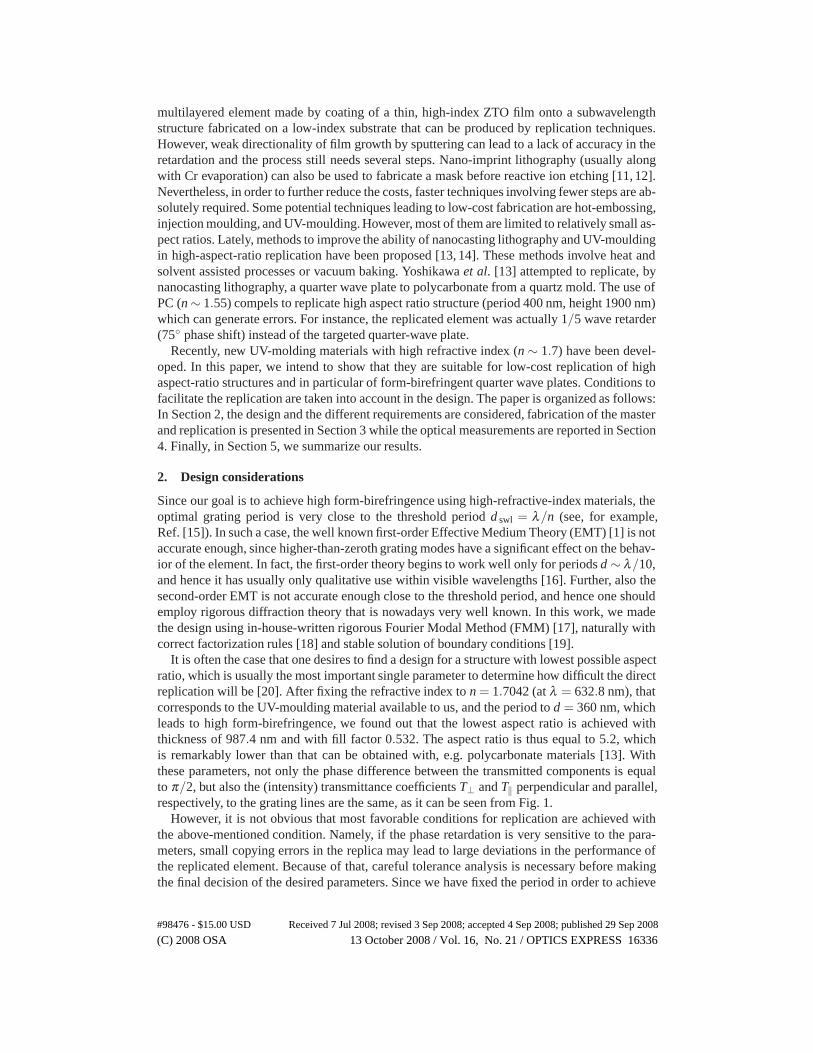
It is often the case that one desires to find a design for a structure with lowest possible aspectratio, which is usually the most important single parameter to determine how difficult the directreplication will be [20]. After fixing the refractive index to n = 1.7042 (at λ = 632.8 nm), thatcorresponds to the UV-moulding material available to us, and the period to d = 360 nm, whichleads to high form-birefringence, we found out that the lowest aspect ratio is achieved withthickness of 987.4 nm and with fill factor 0.532. The aspect ratio is thus equal to 5.2, whichis remarkably lower than that can be obtained with, e.g. polycarbonate materials [13]. Withthese parameters, not only the phase difference between the transmitted components is equalto π/2, but also the (intensity) transmittance coefficients T⊥ and T‖ perpendicular and parallel,respectively, to the grating lines are the same, as it can be seen from Fig. 1.
However, it is not obvious that most favorable conditions for replication are achieved withthe above-mentioned condition. Namely, if the phase retardation is very sensitive to the para-meters, small copying errors in the replica may lead to large deviations in the performance ofthe replicated element. Because of that, careful tolerance analysis is necessary before makingthe final decision of the desired parameters. Since we have fixed the period in order to achieve
#98476 - $15.00 USD Received 7 Jul 2008; revised 3 Sep 2008; accepted 4 Sep 2008; published 29 Sep 2008
(C) 2008 OSA 13 October 2008 / Vol. 16, No. 21 / OPTICS EXPRESS 16336
high form birefringence, only thickness and fill factor are adjusted in the tolerance analysis.The results of the tolerance analysis are summarized in Figs. 1 and 2 that show the variation
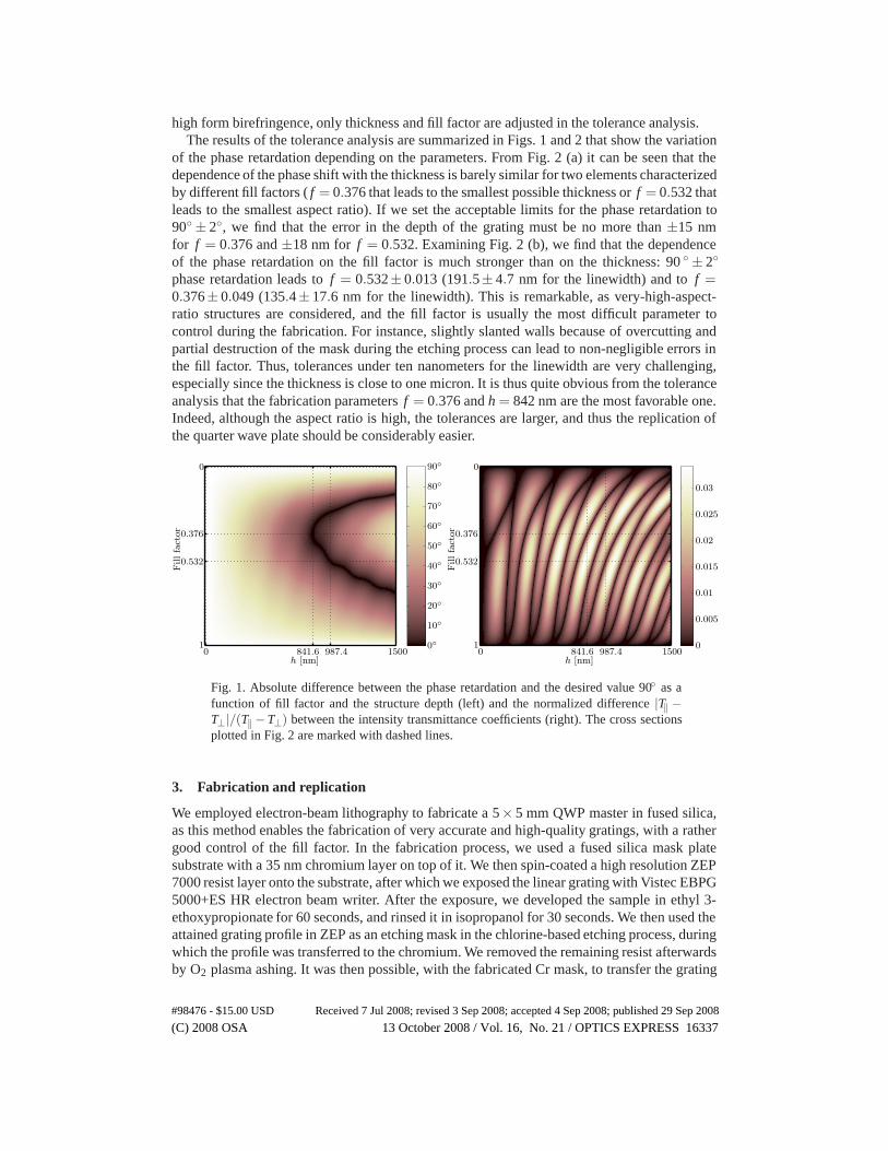
of the phase retardation depending on the parameters. From Fig. 2 (a) it can be seen that thedependence of the phase shift with the thickness is barely similar for two elements characterizedby different fill factors ( f = 0.376 that leads to the smallest possible thickness or f = 0.532 thatleads to the smallest aspect ratio). If we set the acceptable limits for the phase retardation to90◦ ± 2◦, we find that the error in the depth of the grating must be no more than ±15 nmfor f = 0.376 and ±18 nm for f = 0.532. Examining Fig. 2 (b), we find that the dependenceof the phase retardation on the fill factor is much stronger than on the thickness: 90 ◦ ± 2◦phase retardation leads to f = 0.532± 0.013 (191.5± 4.7 nm for the linewidth) and to f =0.376± 0.049 (135.4± 17.6 nm for the linewidth). This is remarkable, as very-high-aspect-ratio structures are considered, and the fill factor is usually the most difficult parameter tocontrol during the fabrication. For instance, slightly slanted walls because of overcutting andpartial destruction of the mask during the etching process can lead to non-negligible errors inthe fill factor. Thus, tolerances under ten nanometers for the linewidth are very challenging,especially since the thickness is close to one micron. It is thus quite obvious from the toleranceanalysis that the fabrication parameters f = 0.376 and h = 842 nm are the most favorable one.Indeed, although the aspect ratio is high, the tolerances are larger, and thus the replication ofthe quarter wave plate should be considerably easier.
0◦
10◦
20◦
30◦
40◦
50◦
60◦
70◦
80◦
90◦
0
0
0
0
0
0.005
0.01
0.015
0.02
0.025
0.03
841.6841.6 987.4987.4
0.3760.376
0.5320.532
1115001500
h [nm]h [nm]
Fillfa
ctor
Fillfa
ctor
Fig. 1. Absolute difference between the phase retardation and the desired value 90◦ as afunction of fill factor and the structure depth (left) and the normalized difference |T‖ −T⊥|/(T‖ −T⊥) between the intensity transmittance coefficients (right). The cross sectionsplotted in Fig. 2 are marked with dashed lines.
3. Fabrication and replication
We employed electron-beam lithography to fabricate a 5× 5 mm QWP master in fused silica,as this method enables the fabrication of very accurate and high-quality gratings, with a rathergood control of the fill factor. In the fabrication process, we used a fused silica mask platesubstrate with a 35 nm chromium layer on top of it. We then spin-coated a high resolution ZEP7000 resist layer onto the substrate, after which we exposed the linear grating with Vistec EBPG5000+ES HR electron beam writer. After the exposure, we developed the sample in ethyl 3-ethoxypropionate for 60 seconds, and rinsed it in isopropanol for 30 seconds. We then used theattained grating profile in ZEP as an etching mask in the chlorine-based etching process, duringwhich the profile was transferred to the chromium. We removed the remaining resist afterwardsby O2 plasma ashing. It was then possible, with the fabricated Cr mask, to transfer the grating
#98476 - $15.00 USD Received 7 Jul 2008; revised 3 Sep 2008; accepted 4 Sep 2008; published 29 Sep 2008
(C) 2008 OSA 13 October 2008 / Vol. 16, No. 21 / OPTICS EXPRESS 16337
700 750 800 850 900 950 1000 1050 110070
75
80
85
90
95
100
105
110
0.2 0.3 0.4 0.5 0.6 0.765
70
75
80
85
90
95
100
105
Thickness [nm]
Phase
shift
[◦]
f = 0.376f = 0.532
Fill factor
(a) (b)
Phase
shift
[◦]
h = 841.6 nmh = 987.4 nm
Fig. 2. Variations of the phaseshift when the thickness (a) and the fill factor (b) vary. Thedashed curve described the case where the lowest aspect ratio has been taken as an op-timization parameter while the solid curve described the case where the thickness is theoptimization parameter.
profile into the substrate material by trifluoromethane (CHF3) based etching process. Finally,after removing the extant chromium by wet etching, the grating profile in silicon dioxide wasattained, as it can be seen in Fig. 3.
Fig. 3. The master structure of QWP fabricated to silicon dioxide by electron beam lithog-raphy and chlorine and CHF3 based etching.
We prepared the master for replication by applying an anti-adhesive surface treatment. Theperformed treatment is based on liquid-phase deposition of alkyltrichlorosilane, which mod-ifies the surface energy, making the quartz surface hydrophobic and therefore more suitablefor copying [21]. First, the master is immersed in the solution of HFE7100 solvent (3M)and tridecafluoro-1,1,2,2-tetrahydrooctyl-trichlorosilane (1000 ml/2 ml) for 15 min. Then itis rinsed in pure HFE7100 solvent for another 15 min and dried in a strong nitrogen flow. Thewhole process is performed under nitrogen atmosphere because of the high reactivity of thesilane.
As mentioned in preceding section, the master structure is in the scale of hundred nanome-ters and the aspect ratio is relatively high (∼ 6). These characteristics cause special challengesfor the replication technique in filling of the structure and demoulding of the replica. There-fore, the chosen replication method is the UV-replication by liquid UV-curable prepolymers. Inthis study, the UV-moulding of QWP nano-structure is performed by EVG520 UV-embossingequipment from EV Group by using a novel optical polymer from Mitsubishi Gas Chemical.
#98476 - $15.00 USD Received 7 Jul 2008; revised 3 Sep 2008; accepted 4 Sep 2008; published 29 Sep 2008
(C) 2008 OSA 13 October 2008 / Vol. 16, No. 21 / OPTICS EXPRESS 16338
The replication polymer is a new Lumiplus material which has high optical clarity and highrefractive index (n = 1.7042 at λ = 632.8 nm) in visible wavelength band and hence it is op-timal for the class of components considered here [22]. The UV-material is made of a mixtureof three components (monomer, catalyte, and photo initiator) whose self-life in liquid-form is6–10 hours, and therefore it needs to be mixed just before the replication process [23]. In roomtemperature, the liquid Lumiplus UV-material has also optimal 20 cps viscosity that can be de-creased by heating during the replication process in order to improve the filling of the structure.The substrates for the replicated component is made from similar Lumiplus material.
In the replication process, the liquid Lumiplus material is dispensed on the master and theLumiplus substrate is laid on the top. The stack is heated in the embosser chamber at 40 ◦Ctemperature and pressed together with an uniform 3400 N pressing force for a 4”×4” substratearea by a wedge compensated piston. The pressure is applied for 10 seconds before the expo-sure when the dispensed droplet of UV-material is spread between the master and substrate andhas filled the structure properly. Despite the low viscosity of the UV-material, the hydrophobicsurface and nanostructure surface properties avoid a proper filling of the UV-material. Conse-quently, replication equipment with high pressing force is essential. The pressure is held untilthe hardening of the copy with 3700 mJ/cm 2 UV-dose is done. The light source used in theprocess is a 400 W Metal Halide Lamp with intensity > 70 mW/cm2 for wavelengths 300–500nm.
After the exposure cycle, substrate and replicated structure are peeled off from the master.Owing to the high aspect ratio, the demolding is very sensitive to the separation techniquebecause of relatively high adhesion in the grating area despite the anti-adhesion layer on themaster surface. Moreover, the adhesion difference between the structure area and the clearmaster surface is remarkable and hence the separation tends to be uneven. Consequently, with-out precautions, the replica and the master are separated with locally progressive boundarystarting from the center to the border of the element [Fig. 4 (a)]. Moreover, if the direction ofthis boundary differs strongly from the direction of the grating lines, the replicated structuresmay suffer from mechanical stress which may cause breaking of the replicated grating lines[Fig. 4 (b)]. Figure 4 (c) shows SEM pictures of elements presenting such a behavior during thedemolding process.
In order to avoid the aforementioned drawbacks, we performed demolding by applying theopening force locally to the grating area. At the same time, the surrounding area is pressedagainst the master until the grating area is separated simultaneously. With this technique, weobtained successful replicas. We inspected the quality of the replicated structures carefully bySEM, and found no defects in the 5×5 mm surface area. Figure 5 shows examples of the resultsof successful replication.
4. Optical measurements
We performed the optical measurements of different replicas with a HeNe laser (λ = 632.8 nm)using a quarter-wave-plate method: The incident linearly polarized electric field is input tothe system formed by the element to be measured, followed by a quarter-wave plate and ananalyzer. The grating vector of the element is set to 45 ◦ with respect to the plane of vibrationof the input field, whereas the fast axis of the quarter-wave plate is set parallel to the input-fieldpolarization. The rotation angle of the analyzer is denoted by θ . The Jones vector of the output
#98476 - $15.00 USD Received 7 Jul 2008; revised 3 Sep 2008; accepted 4 Sep 2008; published 29 Sep 2008
(C) 2008 OSA 13 October 2008 / Vol. 16, No. 21 / OPTICS EXPRESS 16339
(a)
(b)
(c)
Fig. 4. Sketch of the separation or demolding issue. When the force is applied to one point,the separation boundary does not remain perpendicular to the grating lines (a) and maycause breaking of the lines (b). (c) SEM image of one of the first replicas. A more elaboratedseparation technique has been developed in order to avoid this kind of effects, as describedin the text.
Fig. 5. UV replica of the QWP master element.
electric field thus assumes a form [24]
J(θ ) =12
[cos2 θ cosθ sinθ
cosθ sinθ sin2 θ
][1 00 i
][t⊥ + t‖ t⊥− t‖t⊥− t‖ t⊥ + t‖
][10
]
=12[t⊥ exp(iθ )+ t‖ exp(−iθ )]
[cosθsinθ
](1)
where t⊥ and t‖ denote the complex-amplitude transmittance coefficients in directions paralleland perpendicular to the grating vector, and we have normalized the amplitude of the incident
#98476 - $15.00 USD Received 7 Jul 2008; revised 3 Sep 2008; accepted 4 Sep 2008; published 29 Sep 2008
(C) 2008 OSA 13 October 2008 / Vol. 16, No. 21 / OPTICS EXPRESS 16340
field to unity. The output intensity thus assumes the form
I(θ ) =14(|t⊥|2 + |t‖|2)+
12|t⊥||t‖|cos(2θ −Δα), (2)
where Δα = arg(t‖)− arg(t⊥) is the unknown value of the phase retardation. It can be thusdetermined very accurately by finding the value θ = θ min for which the intensity reaches itsminimum value Imin = (|t⊥|− |t‖|)2/4. Thus, the value of the intensity minimum also gives usthe (relative) difference between the transmission coefficients.
We carried out the measurements for different elements characterized by slightly differingfill factors, as well as different replicas of the same master element. In fact, we varied thedoses during the exposure step by step in order to investigate the behavior of the elements asa function of fill factor. The results are in excellent agreement with the theoretical predictions.The best element leads to 90◦ phase retardation with equal transmission coefficients in twodirections. The measurement accuracy is estimated to be better than 1%. We also cut someof the replicated elements, and performed analysis of the actual structure shape by SEM. Wefound that the fill factor of the best element is around 0.38 that was also our target value (line-width varies from 120 nm to 150 nm from up-part to bottom-part of the grating). In this case, thevalued of phase retardation varied from 87 ◦ to 90◦ depending on the replica made from the samemaster element. For the other elements, we found that the phase retardation varied between 75 ◦and 85◦. For instance, one element whose fill factor was afterwards found to be equal to 0.42led to 83–86◦ phase retardation, while another element whose fill factor was measured to bearound 0.47 led to 75–80◦ phase retardation. The values of the phase retardation are slightly(few degrees) lower than what could be expected (Fig. 2), because few tens of nanometers aremissing from the depth.
In addition to the measurements of the phase retardation, Fig. 6 (a) shows the transmissionafter the analyzer behind the elements as a function of the rotation angle of the analyzer. It isobvious that, along with a correct phase retardation (measured by the quarter-wave plate methoddescribed above), the third element produces a perfectly circularly polarized wave. With form-birefringent elements, the phase retardation is a crucial point but the transmission values for thedifferent components are also very important. If the shape is not accurate, phase-shift variationsare followed by variations in the transmission, which explains why the transmission after theanalyzer varies quickly from one element to another even though the phase retardation does notvary remarkably.
Concerning the different replicated elements, we observed variations up to 5 ◦ between tworeplicas of the same master element. This happens when the fill factor is too high, since thephase retardation is very sensitive with the fill factor, as shown in Fig. 2. However, when thefill factor value allows to be in the “high-tolerance region”, variations up to only 3 ◦ [Fig. 6 (b)]have been measured, showing the importance of the replication considerations in the design ofthe elements. Indeed, in this case, small variations of the profile between the different replicasdo not lead to intolerable variations in the phase retardation. It can also be noted that eachelement has been tested at different points of its surface and the same results were observed.
5. Conclusions
This study deals with straight replication, suitable for mass production, of form-birefringentquarter-wave plates by UV-moulding process. Because of high aspect ratios, correct replicationof such elements is very challenging and, to the best of our knowledge, this paper reports thefirst successful demonstration of single-element quarter-wave plates by single-step replicationtechnique. In this paper, new UV-curable replication material characterized by high refrac-tive index n = 1.704 (allowing significant reduction of the aspect ratio) is utilized to produce
#98476 - $15.00 USD Received 7 Jul 2008; revised 3 Sep 2008; accepted 4 Sep 2008; published 29 Sep 2008
(C) 2008 OSA 13 October 2008 / Vol. 16, No. 21 / OPTICS EXPRESS 16341
0 20 40 60 80 100 120 140 160 1800
0.1
0.2
0.3
0.4
0.5
0.6
0.7
0.8
0.9
1
0 20 40 60 80 100 120 140 160 1800
0.1
0.2
0.3
0.4
0.5
0.6
0.7
0.8
0.9
1
Analyzer orientation [◦]
Norm
alize
danaly
zer
transm
itta
nce
SubstrateEl.1: φ = 79◦El.2: φ = 83◦El.3: φ = 90◦
Analyzer orientation [◦]
(a) (b)
Norm
alize
danaly
zer
transm
itta
nce
SubstrateEl.3, repl. 1El.3, repl. 2El.3, repl. 3
Fig. 6. Power measured after the analyzer. (a) without any element or with replicated ele-ments whose introduced phase shift was measured to be around 79◦, 83◦ and 90◦. The lastreplica is very close to a perfect QWP, i.e. intended to create a perfectly circularly polar-ized beam whose transmission through a polarizer is constant when the latter is rotated. (b)without any element or from three different replicas of the best element. There are slightvariations corresponding to around 3◦ variations of the phase retardation.
quarter-wave plate elements. Moreover, a design made using rigorous diffraction theory is pre-sented which allows larger tolerances. The large tolerances also lead to good reproducibilityof the replicated elements originating from the same master. The measurements show that theoptical performance of the replicas is very high: the best replicas lead to 90 ◦ phase retardationand practically equal transmission coefficients along the axes of the element.
Acknowledgments
The work was supported by the Academy of Finland (grants 111701, 118951, and 207523).The authors acknowledge the support of the Network of Excellence in Micro-Optics (NEMO).The funding from the National Agency of Finland (TEKES) (project Hippo) as well as from theMinistry of education (The Research and Development Project on Nanophotonics) is gratefullyappreciated. The authors wish also to thank Sami Hassinen and Victor Prokofiev for technicalassistance.
#98476 - $15.00 USD Received 7 Jul 2008; revised 3 Sep 2008; accepted 4 Sep 2008; published 29 Sep 2008
(C) 2008 OSA 13 October 2008 / Vol. 16, No. 21 / OPTICS EXPRESS 16342