Low-Cost One-Chip Multi-Effects DSP V1000 1 1. General Description With 16 built-in reverb and multi-effects, the V1000 Digital Multi-Effects DSP delivers outstanding audio performance in a rapid time-to-market solution at a very affordable price. Since the V1000 incorporates its own RAM and on-board effects, a complete reverb system can be designed with only the V1000, a low-cost ADC and DAC, and a simple 4-bit controller such as a rotary encoder etc. 2. Features • 16 internal ROM programs consisting of effects such as multiple reverbs, echo, phaser, chorus, flanger, etc. • Serially programmable SRAM (Writeable Control Store - WCS) for program development or dynamically changing programs • Programs run at 128 instructions per word clock. (6 MIPS @ 48 khz sampling frequency) • 32k location Static Ram provides over 0.68 sec of delay at 48 kHz sampling frequency • Package outline: SOIC-16/300 • ROHS compliant (PB-free) V1000 0450A Information furnished by CoolAudio is believed to be accurate and reliable. However, no responsibility is assumed by CoolAudio for its use, nor for any infringements of patents or other rights of third parties which may result from its use. No license is granted by implication or otherwise under any patent or patent rights of CoolAudio. Rev. 1.0
Transcript
Low-Cost One-Chip Multi-Effects DSP
V1000
1
1. General Description
With 16 built-in reverb and multi-effects, the V1000 Digital Multi-Effects DSP delivers outstanding audio performance in a rapid time-to-market solution at a very affordable price. Since the V1000 incorporates its own RAM and on-board effects, a complete reverb system can be designed with only the V1000, a low-cost ADC and DAC, and a simple 4-bit controller such as a rotary encoder etc.
2. Features
• 16 internal ROM programs consisting of effects such as multiple reverbs, echo, phaser, chorus, flanger, etc.• Serially programmable SRAM (Writeable Control Store - WCS) for program development or
dynamically changing programs• Programs run at 128 instructions per word clock. (6 MIPS @ 48 khz sampling frequency)• 32k location Static Ram provides over 0.68 sec of delay at 48 kHz sampling frequency• Package outline: SOIC-16/300• ROHS compliant (PB-free)
V1000
0450A
Information furnished by CoolAudio is believed to be accurate and reliable. However, no responsibility is assumed by CoolAudio for its use, nor for any infringements of patents or other rights of third parties which may result from its use. No license is granted by implication or otherwise under any patent or patent rights of CoolAudio.
Rev. 1.0
V1000
2
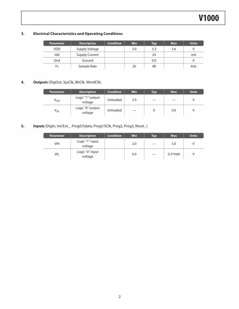
3. Electrical Characteristics and Operating Conditions
Int/Ext_, prog0, prog1, prog2 and prog3 are pulled up to Vdd via nominal internal 30k resistor.
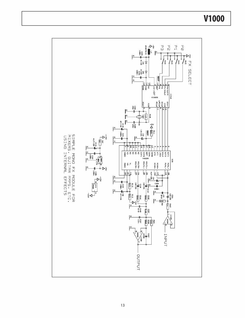
7. Block Diagram
Pin# Name PinType Description
1 DigOut Output Digital serial output for stereo DAC
2 Int/Ext_ Input Internal/external program selection
3 XtalIn Input 12.288 MHz crystal input
4 XtalOut Output 12.288 MHz crystal output
5 Prog0/SData InputInternal program select0/serial
interface data line
6 Prog1/SClk InputInternal program select1/serial
interface clock line
7 Prog2 Input Internal program select2
8 Prog3 Input Internal program select3
9 WordClk Output Word clock output
10 BitClk Output Bit clock output
11 SysClk Output System clock output
12 Reset_ Input Active low reset
13 Gnd Ground Ground connection
14 Vdd Power Vdd power pin
15 NC
16 DigIn Input Digital serial input for stereo ADC
DigOutOUTPUT
REGISTER
MAC
MUX
Data RAM
AddressGenerator
Add
ress
Gen
erat
or
ProgramROM
Controller
Dec
ode
WCS RAM
ClockGenerator
SerialInterface
LFO0
LFO1
LFO2
LFO3
Xtal IN WdClkBitClkSysClk
Systemclock
Xtal OUT
SDataSClkDigIn
Prog0Prog1
Prog2
Prog3
Int/Ext
V1000
4
8. Internal Programs
The SCR comes with 16 internal ROM programs ready to go. By setting the chip to internal mode, the four program pins may be used to select between the different algorithms.
9. Programming the RAM
Alongside the 16 internal programs is an externally programmable SRAM that is easily accessible through the serial clock and data pins, by setting the chip to external mode, the SClk and SData pins become available for serial communication. Except for its external programmability, there is no functional difference between the SRAM and the internal ROMs.
10. Memory Map
Prog[3:0] Name Description
0000 Medium Reverb, Small hall (1.5 sec.)
0001 Chambr7b Reverb, Big hall (2.8 sec.)
0010 Room3b Reverb, Room (1.8 sec.)
0011 Chamber2 Reverb, Church (7 sec.)
0100 Revers3b Reverb Reverse (1.2 sec.)
0101 Gated4b Reverb Gated (0.8 sec.)
0110 Room2a Reverb Chapel (3 sec.)
0111 Spring3b Reverb Spring (2 sec.)
1000 Phaser1 Phaser
1001 Flanger2 Flanger
1010 Delay7 Echo
1011 Chorus4 Chorus
1100 Earlref4 Early Reflection
1101 Amb4 Big Ambience
1110 Delay3 Stereo Delay
1111 Delay1 Slap-back Delay
Addr Name
0.127 WCS RAM
Addr Name
0:3 LFO Coefficients
4:127 MAC Instructions
128 Control/Status 0
V1000
5
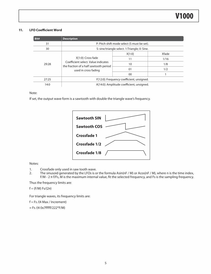
11. LFO Coefficient Word
Note:
If set, the output wave form is a sawtooth with double the triangle wave’s frequency.
Notes:
1. Crossfade only used in saw tooth wave.2. The sinusoid generated by the LFOs is or the formula Asin(nF / M) or Acos(nF / M), where n is the time index,
F/M - 2 π f/Fs, M is the maximum internal value, fit the selected frequency, and Fs is the sampling frequency.
Thus the frequency limits are:
f = (F/M) Fs/(2π)
For triangle waves, its frequency limits are:
f = Fs /(4 Max / Increment)
= Fs /(4 0x7fffff/222*F/M)
Bit# Description
31 P: Pitch shift mode select (S must be set).
30 S: sine/triangle select. 1:Triangle; 0: Sine.
29:28
X[1:0]: Cross fadeCoefficient select. Value indicates
the fraction of a half sawtooth period used in cross fading
X[1:0] Xfade
11 1/16
10 1/8
01 1/2
00 1
27:25 F[12:0]: Frequency coefficient, unsigned.
14:0 A[14:0]: Amplitude coefficient, unsigned.
Sawtooth SIN
Sawtooth COS
Crossfade 1
Crossfade 1/2
Crossfade 1/8
V1000
6
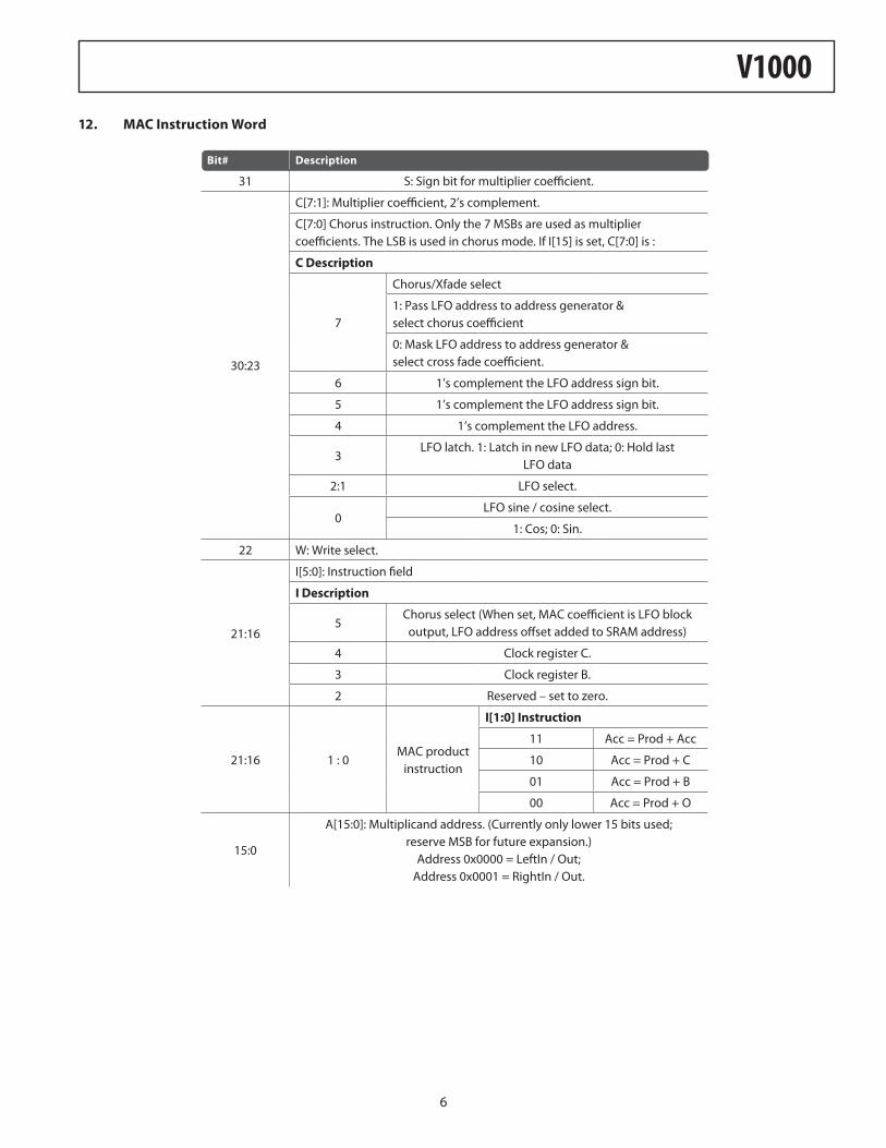
12. MAC Instruction Word
Bit# Description
31 S: Sign bit for multiplier coefficient.
30:23
C[7:1]: Multiplier coefficient, 2’s complement.
C[7:0] Chorus instruction. Only the 7 MSBs are used as multiplier coefficients. The LSB is used in chorus mode. If I[15] is set, C[7:0] is :
1. This complement is only for the MSB, and sign-extension bits are not affected.2. The LeftOut, RightOut, and C registers are in parallel with the accumulator, and will contain the same value
as the accumulator if clocked at the end of the tick. Thus, a write to LeftOut or RightOut will store the current tick’s results.
3. A write to SRAM stores the last tick’s results into address A. During writes, the multiplicand is set to be the Acc, since A[15:0] is used for the excursion address. Writes to LeftOut or RightOut can use the Acc = Product + Acc instruction with the multiplier coefficient set to 0 to pass all bits unaltered.
4. Register B, if clocked at the end of the tick, will store the value of the current tick’s multiplicand. When a read is executed, B latches LeftIn, RightIn, or SRAM. When a write is executed, B latches the accumulator from the last tick.
5. The accumulator contains the result from the last instruction tick, and is updated at the end of the current instruction tick.
6. The internal SRAM address offset automatically decrements by 1 every word clock period.7. Because addresses 0x0000 and 0x0001 are being used to access the left and right channels, those SRAM
memory locations may not be directly written to or read from.
13. Control / Status Word 0
14. Instruction Set
LFO Declarations
The LFOs must be set up with operating parameters if you want to use them. These include amplitude and frequency coefficients, and waveform selection. The setup information for the four LFOs occupy the first four ticks in the program RAM, but the LFO setup declarations may be anywhere in the input file.
The first three statements are required in the order given. The chorus controls and optional statements may then follow in any order, although for readability the above convention should be followed.
DATA Memory Access
The MEM instruction creates a block of memory from the free memory stack. The ABS instruction specifies one particular address, useful for buffers that only require one memory location.
One sample of delay requires 2 memory locations, 10 samples of delay requires 11 memory locations, etc. Memory is allocated from the free memory stack as it is requested
Examples:
MEM delay 1024; 1024 location delay block.
MEM buff3 0x0400; 1024 location buffer.
ABS store 2; Storage location at address 2.
ABS temp2 0x7FFF; Temporary storage at address 32767.
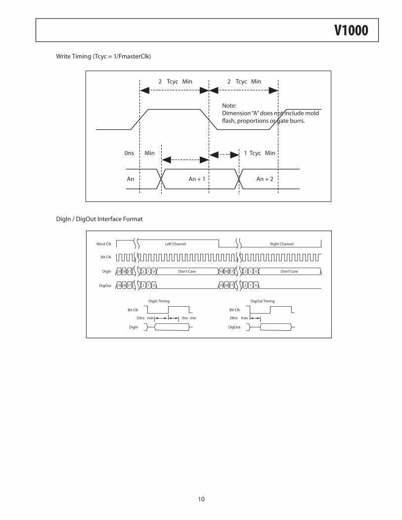
15. Serial Interface Format
The basic format for the micro serial interface is: