1 Revision 1.0, 2014-12-20 About this document Scope and purpose This application note describes Infineon’s GPS/GLONASS/COMPASS MMIC: BGA824N6 used as LNA for LTE band-11 and band-21 applications. 1. This application note documents the design of a LTE band-11 and band-21 LNA with input matching network. 2. The BGA824N6 is used in this documented design. 3. LTE band-11 and band- 21 are the primary application of this document. 4. This design along with AN403 provides a solution to LTE band-11 and band-21 receivers where a single band LNA MMIC is required. 5. Key performance parameter include Gain = 17.3 dB, NF = 0.7 dB, OIP3 = 17.5 dBm and P1dB = -6.8 dBm for 2.8 V. Silicon Germanium Low Noise Amplifier: BGA824N6 Low Noise Amplifier for LTE band-11 (1475.9MHz – 1495.9MHz) and band-21 (1495.9MHz – 1510.9MHz) Application Note AN403
Transcript
1 Revision 1.0, 2014-12-20
About this document
Scope and purpose
This application note describes Infineon’s GPS/GLONASS/COMPASS MMIC: BGA824N6 used as LNA for LTE
band-11 and band-21 applications.
1. This application note documents the design of a LTE band-11 and band-21 LNA with input matching
network.
2. The BGA824N6 is used in this documented design.
3. LTE band-11 and band- 21 are the primary application of this document.
4. This design along with AN403 provides a solution to LTE band-11 and band-21 receivers where a single band LNA MMIC is required.
5. Key performance parameter include Gain = 17.3 dB, NF = 0.7 dB, OIP3 = 17.5 dBm and P1dB = -6.8
dBm for 2.8 V.
Si l i con Ge rma nium L o w No ise A mpli f i er :
BGA8 24 N6
Lo w N ois e Ampli f i er for L T E b a n d -11
(1 47 5.9 M H z – 1 495. 9 M Hz ) a nd ba nd -21
(1 49 5.9 M H z – 1 510. 9 M Hz )
Application Note AN403
Low Noise Amplifier for LTE band-11 and band-21
Table of Content
Application Note AN403 2 Revision 1.0, 2014-12-20
Table of Content
About this document ................................................................................................................... 1
1 Introduction of Low Noise Amplifier for LTE Single Band ................................................. 4
1.1 Introduction About 3G and 4G ............................................................................................................ 4 1.2 Applications ......................................................................................................................................... 6 1.3 Infineon LNAs for 3G, 4G LTE and LTE-A Applications ....................................................................... 7
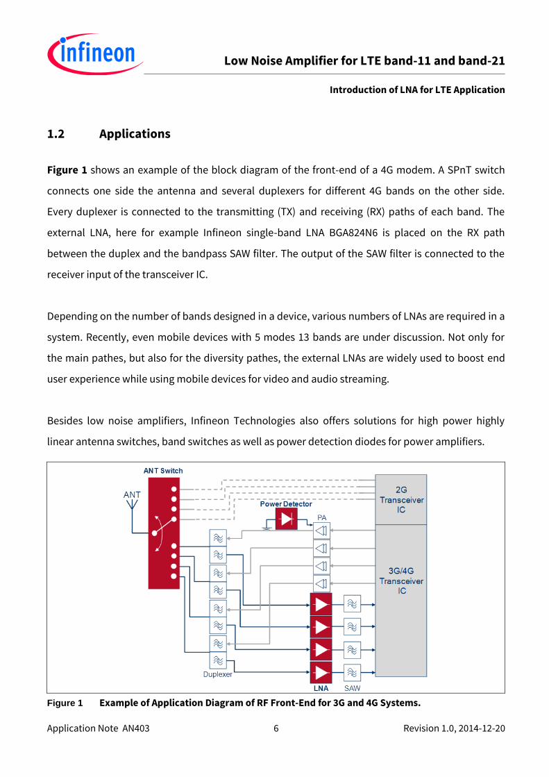
Figure 1 Example of Application Diagram of RF Front-End for 3G and 4G Systems. ....................................... 6
Figure 2 BGA824N6 in TSNP-6-2 ...................................................................................................................... 10 Figure 3 Equivalent Circuit Block diagram of BGA824N6 ............................................................................... 11 Figure 4 Package and pin connections of BGA824N6 .................................................................................... 11 Figure 5 Schematics of the BGA824N6 Application Circuit ........................................................................... 14
Figure 6 Wideband Insertion Power Gain of the BGA824N6 for LTE band-11 and band-21 ......................... 15 Figure 7 Narrowband Insertion Power Gain of the BGA824N6 for LTE band-11 and band-21 ..................... 15
Figure 8 Input Matching of the BGA824N6 for LTE band-11 and band-21 ..................................................... 16
Figure 9 Input Matching (Smith Cahrt) of the BGA824N6 for LTE band-11 and band-21 .............................. 16
Figure 10 Input Matching of the BGA824N6 for LTE band-11 and band-21 ..................................................... 17 Figure 11 Input Matching (Smith Cahrt) of the BGA824N6 for LTE band-11 and band-21 .............................. 17 Figure 12 Reverse Isolation of the BGA824N6 for LTE band-11 and band-21 ................................................. 18
Figure 13 Noise Figure of the BGA824N6 for band-11 and band-21 ................................................................ 18 Figure 14 Stability K Factor and Delta Factor of the BGA824N6 for LTE band-11 and band-21 ..................... 19
Figure 15 Stability μ1 Factor of the BGA824N6 for LTE band-11 and band-21................................................ 19 Figure 16 Stability μ2 Factor of the of the BGA824N6 for LTE band-11 and band-21 ..................................... 20
Figure 17 IP1dB of the BGA824N6 for LTE band-11 .......................................................................................... 20 Figure 18 IP1dB of the BGA824N6 for LTE band-22 .......................................................................................... 21
Figure 19 OIP3 Measurement of the BGA824N6 for LTE band-11 with 1.8 V power supply ........................... 21 Figure 20 OIP3 Measurement of the BGA824N6 for LTE band-11 with 2.8 V power supply ........................... 22
Figure 21 OIP3 Measurement of the BGA824N6 for LTE band-21 with 1.8 V power supply ........................... 22 Figure 22 OIP3 Measurement of the BGA824N6 for LTE band-21 with 2.8 V power supply ........................... 23
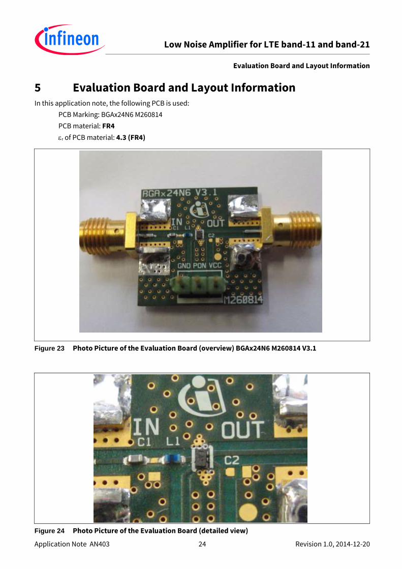
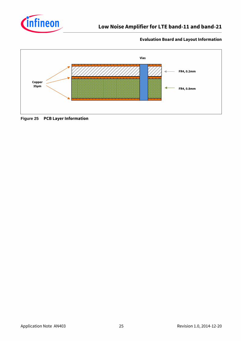
Figure 23 Photo Picture of the Evaluation Board (overview) BGAx24N6 M260814 V3.1 ................................. 24 Figure 24 Photo Picture of the Evaluation Board (detailed view) ................................................................... 24
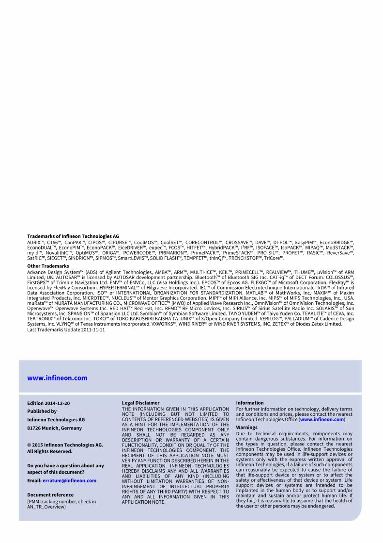
Figure 25 PCB Layer Information ...................................................................................................................... 25
List of Tables Table 2 Infineon Product Portfolio of LNAs for 4G LTE and LTE-A Applications ............................................ 8 Table 3 Infineon Product Portfolio of LNAs for 3G and 4G Applications ........................................................ 9 Table 4 Pin Assignment of BGA824N6 ........................................................................................................... 11
Table 5 Pin Assignment of BGA824N6 ........................................................................................................... 11 Table 6 Electrical Characteristics of the BGA824N6 (at room temperature) ............................................... 12 Table 7 Bill-of-Materials ................................................................................................................................. 14
1) The graphs are generated with the simulation program AWR Microwave Office®.
Low Noise Amplifier for LTE band-11 and band-21
Introduction of LNA for LTE Application
Application Note AN403 4 Revision 1.0, 2014-12-20
1 Introduction of LNA for LTE Application
1.1 Introduction About 3G and 4G
The mobile technologies for smartphones have seen tremendous growth in recent years. The data
rate required from mobile devices has increased significantly over the evolution of modern mobile
technologies, starting from the first 3G/3.5G technologies (UMTS & WCDMA, HSPA & HSPA+) to the
recently 4G LTE-Advanced (LTE-A). LTE-A can support data rates of up to 1 Gbps.
Advanced technologies such as diversity Multiple Input Multiple Output (MIMO) and Carrier
Aggregation (CA) are adopted to achieve such higher data rate requirements. MIMO technology,
commonly referred as the diversity path in smartphones, has attracted attention for the significant
increasement in data throughput and link range without additional bandwidth or increased
transmit power. The technology supports scalable channel bandwidth, between 1.4 and 20 MHz.
The ability of 4G LTE to support bandwidths up to 20 MHz and to have more spectral efficiency by
using high order modulation methods like QAM-64 is of particular importance as the demand for
higher wireless data speeds continues to grow fast. Carrier aggregation used in LTE-Advanced
combines up to 5 carriers and widens bandwidths up to 100 MHz to increase the user rates, across
FDD and TDD.
Countries all over the world have released various frequencies bands for the 4G applications.
Table 1 shows the band assignment for the LTE bands worldwide.
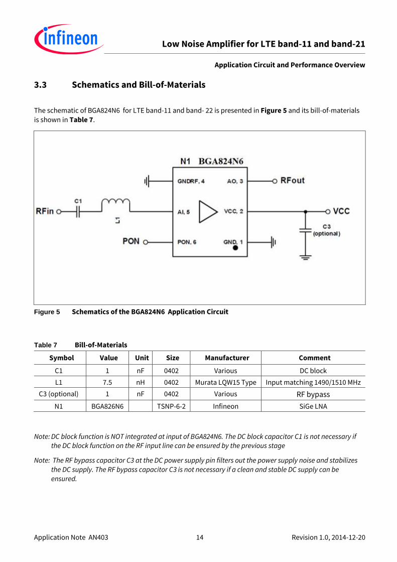
3 Application Circuit and Performance Overview In this chapter the performance of the application circuit, the schematic and bill-on-materials are presented.
Device: BGA824N6
Application: LTE LNA
PCB Marking: BGA824N6
EVB Order No.: AN403
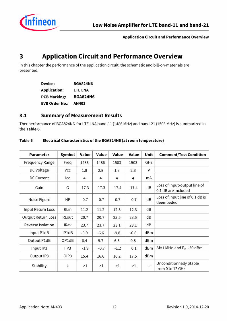
3.1 Summary of Measurement Results
Ther performance of BGA824N6 for LTE LNA band-11 (1486 MHz) and band-21 (1503 MHz) is summarized in the Table 6.
Table 6 Electrical Characteristics of the BGA824N6 (at room temperature)
Parameter Symbol Value Value Value Value Unit Comment/Test Condition
Frequency Range Freq 1486 1486 1503 1503 GHz
DC Voltage Vcc 1.8 2.8 1.8 2.8 V
DC Current Icc 4 4 4 4 mA
Gain G 17.3 17.3 17.4 17.4 dB Loss of input/output line of
0.1 dB are included
Noise Figure NF 0.7 0.7 0.7 0.7 dB Loss of input line of 0.1 dB is
Note: DC block function is NOT integrated at input of BGA824N6. The DC block capacitor C1 is not necessary if the DC block function on the RF input line can be ensured by the previous stage
Note: The RF bypass capacitor C3 at the DC power supply pin filters out the power supply noise and stabilizes
the DC supply. The RF bypass capacitor C3 is not necessary if a clean and stable DC supply can be ensured.
Legal Disclaimer THE INFORMATION GIVEN IN THIS APPLICATION NOTE (INCLUDING BUT NOT LIMITED TO CONTENTS OF REFERENCED WEBSITES) IS GIVEN AS A HINT FOR THE IMPLEMENTATION OF THE INFINEON TECHNOLOGIES COMPONENT ONLY AND SHALL NOT BE REGARDED AS ANY DESCRIPTION OR WARRANTY OF A CERTAIN FUNCTIONALITY, CONDITION OR QUALITY OF THE INFINEON TECHNOLOGIES COMPONENT. THE RECIPIENT OF THIS APPLICATION NOTE MUST VERIFY ANY FUNCTION DESCRIBED HEREIN IN THE REAL APPLICATION. INFINEON TECHNOLOGIES HEREBY DISCLAIMS ANY AND ALL WARRANTIES AND LIABILITIES OF ANY KIND (INCLUDING WITHOUT LIMITATION WARRANTIES OF NON-INFRINGEMENT OF INTELLECTUAL PROPERTY RIGHTS OF ANY THIRD PARTY) WITH RESPECT TO ANY AND ALL INFORMATION GIVEN IN THIS APPLICATION NOTE.
Information For further information on technology, delivery terms and conditions and prices, please contact the nearest Infineon Technologies Office (www.infineon.com).
Warnings Due to technical requirements, components may contain dangerous substances. For information on the types in question, please contact the nearest Infineon Technologies Office. Infineon Technologies components may be used in life-support devices or systems only with the express written approval of Infineon Technologies, if a failure of such components can reasonably be expected to cause the failure of that life-support device or system or to affect the safety or effectiveness of that device or system. Life support devices or systems are intended to be implanted in the human body or to support and/or maintain and sustain and/or protect human life. If they fail, it is reasonable to assume that the health of the user or other persons may be endangered.
Other Trademarks Advance Design System™ (ADS) of Agilent Technologies, AMBA™, ARM™, MULTI-ICE™, KEIL™, PRIMECELL™, REALVIEW™, THUMB™, µVision™ of ARM Limited, UK. AUTOSAR™ is licensed by AUTOSAR development partnership. Bluetooth™ of Bluetooth SIG Inc. CAT-iq™ of DECT Forum. COLOSSUS™, FirstGPS™ of Trimble Navigation Ltd. EMV™ of EMVCo, LLC (Visa Holdings Inc.). EPCOS™ of Epcos AG. FLEXGO™ of Microsoft Corporation. FlexRay™ is licensed by FlexRay Consortium. HYPERTERMINAL™ of Hilgraeve Incorporated. IEC™ of Commission Electrotechnique Internationale. IrDA™ of Infrared Data Association Corporation. ISO™ of INTERNATIONAL ORGANIZATION FOR STANDARDIZATION. MATLAB™ of MathWorks, Inc. MAXIM™ of Maxim Integrated Products, Inc. MICROTEC™, NUCLEUS™ of Mentor Graphics Corporation. MIPI™ of MIPI Alliance, Inc. MIPS™ of MIPS Technologies, Inc., USA. muRata™ of MURATA MANUFACTURING CO., MICROWAVE OFFICE™ (MWO) of Applied Wave Research Inc., OmniVision™ of OmniVision Technologies, Inc. Openwave™ Openwave Systems Inc. RED HAT™ Red Hat, Inc. RFMD™ RF Micro Devices, Inc. SIRIUS™ of Sirius Satellite Radio Inc. SOLARIS™ of Sun Microsystems, Inc. SPANSION™ of Spansion LLC Ltd. Symbian™ of Symbian Software Limited. TAIYO YUDEN™ of Taiyo Yuden Co. TEAKLITE™ of CEVA, Inc. TEKTRONIX™ of Tektronix Inc. TOKO™ of TOKO KABUSHIKI KAISHA TA. UNIX™ of X/Open Company Limited. VERILOG™, PALLADIUM™ of Cadence Design Systems, Inc. VLYNQ™ of Texas Instruments Incorporated. VXWORKS™, WIND RIVER™ of WIND RIVER SYSTEMS, INC. ZETEX™ of Diodes Zetex Limited. Last Trademarks Update 2011-11-11