HAL Id: jpa-00254352 https://hal.archives-ouvertes.fr/jpa-00254352 Submitted on 1 Jan 1996 HAL is a multi-disciplinary open access archive for the deposit and dissemination of sci- entific research documents, whether they are pub- lished or not. The documents may come from teaching and research institutions in France or abroad, or from public or private research centers. L’archive ouverte pluridisciplinaire HAL, est destinée au dépôt et à la diffusion de documents scientifiques de niveau recherche, publiés ou non, émanant des établissements d’enseignement et de recherche français ou étrangers, des laboratoires publics ou privés. Low-Noise Electronics for High-Resolution CdZnTe and CdTe X-Ray Detection Systems A. Niemelä To cite this version: A. Niemelä. Low-Noise Electronics for High-Resolution CdZnTe and CdTe X-Ray Detection Sys- tems. Journal de Physique IV Proceedings, EDP Sciences, 1996, 06 (C4), pp.C4-721-C4-731. 10.1051/jp4:1996469. jpa-00254352
Transcript
HAL Id: jpa-00254352https://hal.archives-ouvertes.fr/jpa-00254352
Submitted on 1 Jan 1996
HAL is a multi-disciplinary open accessarchive for the deposit and dissemination of sci-entific research documents, whether they are pub-lished or not. The documents may come fromteaching and research institutions in France orabroad, or from public or private research centers.
L’archive ouverte pluridisciplinaire HAL, estdestinée au dépôt et à la diffusion de documentsscientifiques de niveau recherche, publiés ou non,émanant des établissements d’enseignement et derecherche français ou étrangers, des laboratoirespublics ou privés.
Low-Noise Electronics for High-Resolution CdZnTe andCdTe X-Ray Detection Systems
A. Niemelä
To cite this version:A. Niemelä. Low-Noise Electronics for High-Resolution CdZnTe and CdTe X-Ray Detection Sys-tems. Journal de Physique IV Proceedings, EDP Sciences, 1996, 06 (C4), pp.C4-721-C4-731.�10.1051/jp4:1996469�. �jpa-00254352�
JOURNAL DE PHYSIQUE IV Colloque C4, suppl6ment au Journal de Physique JII, Volume 6, juillet 1996
Low-Noise Electronics for High-Resolution CdZnTe and CdTe X-Ray Detection Systems
A. ~ieme la ( l )
Metorex International Oy, Riihitontuntie 7 C, P.O. Box 85, 02201 Espoo, Finland
Abstract
CdZnTe and CdTe detector performance can be significantly improved with low-noise electronics. The main sources of noise that broaden the spectrum peaks in a room-temperature system are in- complete charge collection and leakage current of the detector, and the feedback resistor of the preamplifier. The detector leakage current can be reduced by cooling the detector to about -30°C. Normally, at these temperatures the leakage current of a small detector crystal drops to the picoampere level which enables the use of low-noise, pulsed-optical feedback preamplifiers instead of noisier resistive feedback preamplifiers. Also, because of lower leakage currents, it is possible to use higher bias voltages at low temperatures which is important for more efficient charge collection. This reduces spectrum background and peak tailing. Applying rise time discrimination circuitry to the linear amplifier reduces the tailing effect even further, especially at higher energies. By employing all these methods a number of Cdo 9Zno lTe, Cdo sZno 2Te and PIN-structure CdTe detector crystals were tested at temperatures between -20°C and -40°C, and at best FWHM energy resolutions of 240 eV at the 5.9-keV line of 5 5 ~ e , 600 eV at the 59.5-keV line of 2 4 1 ~ m , and 4.4 keV (0.7 %) at the 662-keV line of 1 3 7 ~ s were obtained. These energy resolutions measured at room temperature with conventional methods are typically about 4 to 10 times poorer.
The total energy resolution (FWHM) of an X-ray or gamma-ray detection system at a known radiation energy can be divided in three major contributors, which sum quadratically:
where FWHME is the electronics noise contribution measured as the pulser resolution; FWHMx is the detector noise contribution, or the "tailing factor", due to incomplete charge collection and other non- ideal effects in the detector crystal; and FWHMD is the detector crystal statistical noise contribution, given by:
where F is the Fano factor, E the average energy required to produce an electron-hole pair in the detector material, in eV, and E the radiation energy in eV. The Fano factor is usually 0.10 to 0.12 for good quality silicon and germanium detectors but slightly higher for currently available compound semiconductor detectors.
('I Present address: Massachussetts Institute of Technology, Room 26-552,77 Mass. Ave., Cambridge, MA 02139, U.S.A.
Article published online by EDP Sciences and available at http://dx.doi.org/10.1051/jp4:1996469
When one wants to improve the energy resolution FWHM of an X-ray detection system, one must concentrate on minimizing the electronic noise contribution FWHME because there are no means to reduce the statistical noise contribution FWHMD and methods to affect FWHMX are limited. The various contributors of the electronics noise FWHME are discussed in detail in the next chapter.
The noise due to electronics, i.e. the preamplifier front end and the shaping amplifier, is conveniently calculated with equivalent noise charge (ENC, in rms electrons) which can be divided into three separate contributors:
where ENCsER is the "series noise" contributor including noise sources due to the input FET white voltage noise e,, and the detector and FET capacitances [I]:
where k is Boltzmann's constant (1.38 ~O-~~JIK); T is absolute temperature in K; a, is a noise parameter of the shaping amplifier; is related to the voltage noise of the FET by: e: = 4kTI'lg,,, with a theoretical and typical value of r = 0.67 (however, for short-channel FET's the value can be higher than unity); m = CdC, is the mismatch coefficient for the FET gate capacitance Cg and the detector capacitance CD which is assumed to contain all stray capacitances including the feedback capacitor Cf ; zM is the measurement time, or peaking time of the shaping amplifier (directly proportional to the Gaussian shaping time constant z by: z~ = 2.2%); and o, = gJCg is the cut-off, or transition frequency of the FET.
The second term in Eq. (3) ENCIA describes the noise due to the FET llf noise:
where a2 is another noise parameter of the shaping amplifier, and Hf = Af C, ; with Af related to the Ilf- noise spectral density S(f) = Af If" and a being close to unity. Af is strongly dependent of the operating temperature of the FET [2].
The third term ENCpAR is the "parallel noise" component due to shot noise in the reverse leakage currents of the FET (IG) and the detector (IL), and to the thermal noise of the feedback resistor Rf if one is used in the preamplifier:
where q is the charge of an electron (1.60 lo-'' C). To minimize the effect of the feedback resistor Rf its value must be maximized. However, large value resistors (in the order of G a s ) act as sources of noise far larger than would be expected theoretically in Eq. (6). This is due to the fact that there is some capacitive and sometimes inductive parasitics in large value resistors, and the absolute value of the resistance is often strongly dependent of frequency, voltage and temperature.
The noise parameters (al , a2 and a3 ) of the shaping amplifier vary according to the shaping function used. For instance [I], values of al = 813, a2 = 3.6, a:, = 0.77 can be used for the most commonly used and wide-spread type of nuclear spectroscopy linear shaping amplifier, the Gaussian one.
The effect of the mismatch coefficient m = CdC, is at its minimum when the FET gate capacitance equals the detector capacitance. Therefore, the input FET should be chosen so that it is frstly as low- noise as possible, and secondly matches the detector capacitance as closely as possible. Selected devices like Motorola 2N4416 (Cg = 3.5 pF, gm = 7 mAN, q, = 1.3 n~/dHz), InterFET NJ14 (C = 2.5 pF, g, =
6 mAN, en = 1.5 n~ldHz) and Moxtek MXlO (C, = 0.8 pF, gm = 7 mAN, en = 1.3 n~/$Hz) have been found to be suitable for operation with low-capacitance detectors at room temperature, and at lower temperatures.
There are other sources of noise present in an X-ray detection system than the ones described above, for example, "microphonics" due to mechanical vibration of the FET gate lead or components operated at high-voltage, llf noise and gate-coupled thermal noise of the FET, and dielectric noise due to, for instance, dielectric losses in the materials that are physically in connection with the detector or the FET gate. Care must be taken when mounting the detector crystal and the FET on a substrate or package. High-purity Teflon, sapphire, boron nitride and alumina have been found to be good mounting materials for the front end. For instance, if optimally high resolution is required, the FET should be removed from its original can or package and mounted on low-loss, low-leakage material. The dark glass-like material found underneath a metallic FET can is a relatively high source of excess noise. Similarly, the feedback capacitor Cf should be made of good, low-loss dielectric. Also, care must be taken not to add any unwanted parasitic stray capacitance in parallel with the detector-FET node when designing the front end. If these precautions are taken into account, the noise sources mentioned above are not important in a real-life system and are not considered mathematically here. However, a more detailed discussion of some of these additional sources of noise can be found in Ref. [I] or [2].
The ENC formula (3) gives the electronic noise of the system in "rms electrons". However, usually it is clearer and more convenient to give the electronic noise in eV with the help of FWHME , which is called the "pulser resolution" of the system:
FWHME = 2.3 5 ENC &/q (7)
where E is the average energy required to create an electron-hole pair in the detector material and q is the charge of an electron. For example, for Cdo,8Z@,2Te E is assumed to be 5.0 eV, for CdTe the value is 4.43 eV, and for silicon 3.61 eV at room temperature.
As a mathematical example we can calculate the electronic noise, or pulser resolution FWHME of a good-quality, low-leakage current CdZnTe X-ray detection system at various shaping time constants. Let us assume that the detector size is 2x2~2 mm3 (CD = 0.4 pF, IL = 500 PA) and it is used at room temperature with a resistive feedback preamplifier employing a 2N4416-type FET (C = 3.5 pF, g, = 7
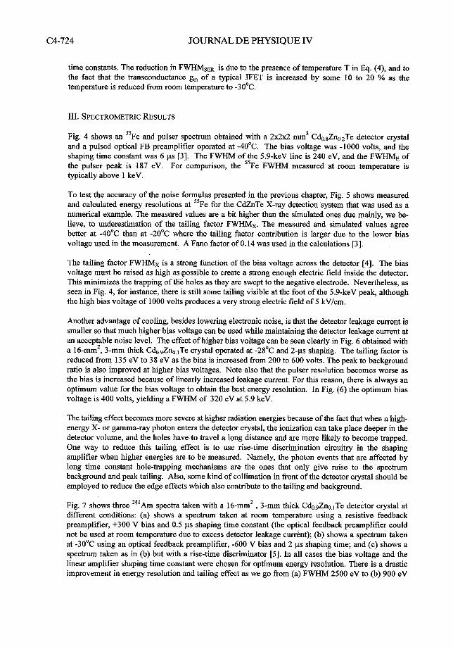
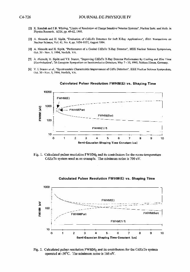
27 7! mAN, o, = g,/C, = 2 10' radfs, IG = 0.2 PA, Af = 10'15 v', Hf = A&, = 3.5 10- V F) and a feedback resistor Rf = 10 GO. The calculated FWHME with its contributors are displayed graphically in Fig. 1, where the minimum electronic noise of 700 eV is achieved at 0.25-p shaping time constant. As can be seen, the parallel noise contributor FWHMPm totally dominates the noise behavior of the system. Let us consider another case where the same system as above is used with a pulsed optical feedback preamplifier with the FET and detector cooled to -30°C (T = 243 K). The nurrierical values for this case are the same, except for: I' = 2 PA, IG = 0.02 pA and Rf = a, all present in the same contributor ENCPAR. The calculated values are presented in Fig. 2. Now the minimum electronic noise is only 166 eV and it is obtained with 5-ps shaping time constant due to the drastically reduced effect of the parallel noise contribution FWHMPm.
To demonstrate the effect of reduced temperature in real life, the pulser resolution FWHME of a 2 x 2 2 mm3 C d o . 8 Z ~ zTe detector crystal was measured at -20, -30 and -40°C with an optical FB preamplifier and a semi-gaussian linear amplifier operated at various shaping time constants. The results are presented in Fig. 3. Note that the parallel noise contribution FWHMPAR is reduced a great deal as we go down in temperature, but only a slight reduction is seen in the series noise FWHMsER at shorter shaping
C4-724 JOURNAL DE PHYSIQUE IV
time constants. The reduction in FWHMsER is due to the presence of temperature T in Eq. (4), and to the fact that the transconductance g, of a typical JFET is increased by some 10 to 20 % as the temperature is reduced from room temperature to -30°C.
Fig. 4 shows an " ~ e and pulser spectrum obtained with a 2 ~ 2 x 2 mm3 CdoBZno2Te detector crystal and a pulsed optical FB preamplifier operated at -40°C. The bias voltage was -1000 volts, and the shaping time constant was 6 ps [3]. The FWHM of the 5.9-keV line is 240 eV, and the FWHME of the pulser peak is 187 eV. For comparison, the " ~ e FWHM measured at room temperature is typically above 1 keV.
To test the accuracy of the noise formulas presented in the previous chapter, Fig. 5 shows measured and calculated energy resolutions at 5 5 ~ e for the CdZnTe X-ray detection system that was used as a numerical example. The measured values are a bit higher than the simulated ones due mainly, we be- lieve, to underestimation of the tailing factor F W x . The measured and simulated values agree better at -40°C than at -20°C where the tailing factor contribution is larger due to the lower bias voltage used in the measurement. A Fano factor of 0.14 was used in the calculations [3].
The tailing factor FWHMX is a strong function of the bias voltage across the detector [4]. The bias voltage must be raised as high as possible to create a strong enough electric field inside the detector. This minimizes the trapping of & holes as they are swept to the negative electrode. Nevertheless, as seen in Fig. 4, for instance, there is still some tailing visible at the foot of the 5.9-keV peak, although the high bias voltage of 1000 volts produces a very strong electric field of 5 kV1cm.
Another advantage of cooling, besides lowering electronic noise, is that the detector leakage current is smaller so that much higher bias voltage can be used while maintaining the detector leakage current at an acceptable noise level. The effect of higher bias voltage can be seen clearly in Fig. 6 obtained with a 16-mm2, 3-mm thick Cdo9Zno.lTe crystal operated at -2S°C and 2-ps shaping. The tailing factor is reduced from 135 eV to 38 eV as the bias is increased from 200 to 600 volts. The peak to background ratio is also improved at higher bias voltages. Note also that the pulser resolution becomes worse as the bias is increased because of linearly increased leakage current. For this reason, there is always an optimum value for the bias voltage to obtain the best energy resolution. In Fig. (6) the optimum bias voltage is 400 volts, yielding a FWHM of 320 eV at 5.9 keV.
The tailing effect becomes more severe at higher radiation energies because of the fact that when a high- energy X- or gamma-ray photon enters the detector crystal, the ionization can take place deeper in the detector volume, and the holes have to travel a long distance and are more likely to become trapped. One way to reduce this tailing effect is to use rise-time discrimination circuitry in the shaping amplifier when higher energies are to be measured. Namely, the photon events that are affected by long time constant hole-trapping mechanisms are the ones that only give raise to the spectrum background and peak tailing. Also, some kind of collimation in front of the detector crystal should be employed to reduce the edge effects which also contribute to the tailing and background.
Fig. 7 shows three 2 4 1 ~ m spectra taken with a 16-mm2 , 3-mm thick Cdo9Zno lTe detector crystal at different conditions: (a) shows a spectrum taken at room temperature using a resistive feedback preamplifier, +300 V bias and 0.5 ps shaping time constant (the optical feedback preamplifier could not be used at room temperature due to excess detector leakage c w h t ) ; (b) shows a spectrum taken at -30°C using an optical feedback preamplifier, -600 V bias and 2 ps shaping time; and (c) shows a spectrum taken as in (b) but with a rise-time discriminator [5]. In all cases the bias voltage and the linear amplifier shaping time constant were chosen for optimum energy resolution. There is a drastic improvement in energy resolution and tailing effect as we go from (a) FWHM 2500 eV to (b) 900 eV
to (c) 600 eV. However, the photopeak counting efficiency dropped to about 50% from (b) to (c) because of the counts rejected by the rise-time discriminator. Note that rise-time discriminator can also correct some more serious charge collection problems, like a localized trap center producing doublet peaks in the energy spectrum [5].
The rise-time discrimination circuitry that was used in the measurements was built around a commercially available gated integrator, in which the voltage pulses with fast rise times reach the flat-top level in a shorter time than pulses that have experienced charge trapping. The pulses with slow rise times are thus gated out of the amplifier output by the control logic. However, the system can also be operated in a correction mode where the slow rise-time pulses are analyzed and placed to the correct channel in the energy spectrum by correction logic circuitry. The operation of the rise- time discriminator is discussed in more detail in Ref. [6].
To demonstrate the high-energy gamma-ray detection performance of the system a 1 3 7 ~ s spectrum was measured with the rise-time discriminator turned off, Fig. 8 (a); and on, Fig. 8 (b). The FWHM of the 662-keV eak was improved from 35 keV to 4.4 keV by the rise-time discriminator. The detector was P a 16-mm ,3-mm thick Cdo9Zno ,Te detector operated at -30°C, -800 V of bias, and 1-ps shaping time constant.
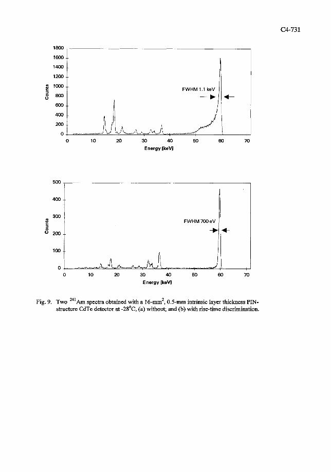
Fig. 9 shows two 2 4 1 ~ m spectra taken at - 2 8 ' ~ with a 16-mmz, 0.5-mm intrinsic layer thickness PIN- structure CdTe detector. The spectrum in Fig. 9 (a) was taken without the rise-time discriminator and Fig. 9 (b) with it. In both measurements the detector bias voltage was -140 volts and the linear amplifier was operated at 2-ps shaping time constant. The 2 4 1 ~ m 59.5-keV line FWHM improved from 1.1 keV to 700 eV, and once again, there is a clearly visible improvement in the peak tail.
IV. CONCLUSIONS
The performance of CdZnTe and CdTe detectors can be significantly improved by low-noise electronics and by cooling the detector and first stage of the preamplifier to a temperature around -30°C which is easily achieved, for example, with commercially available miniature Peltier coolers.
Currently available CdZnTe and CdTe material suffers from charge trappingtdetrapping mechanisms and low hole mobility-lifetime product. Because of this, there is a lot of rise time variations at the preamplifier output, and the slow rise-time pulses are seen lower than correct amplitude at the A D converter input. This increases background and peak tailing in the energy spectrum significantly. However, this effect can be corrected to some extent by applying a rise-time discriminator in the system, although a reduction in the counting efficiency is seen.
I would like to thank Bruce Glick and Kevin Parnharn of eV Products and Jack Butler of Aurora Technologies Corp. (presently Digirad) for supplying the CdZnTe detector crystals for this study, and Victor Ivanov of Baltic Scientific Instruments for supplying the CdTe detectors.
VI. REFERENCES
[ I ] P.F. Manfredi and V. Speziali, "High Density Monolithic Front-End Systems for Detectors without Charge Multiplication", Nuclear Instr. and Meth. in Physics Research, A279, pp. 152-168, 1989.
04-726 JOURNAL DE PHYSIQUE IV
[2] K. Kandiah and F.B. Whiting, "Limits of Resolution of Charge Sensitive Detector Systems", Nuclear Insh. and Meth. in Physics Research, A326, pp. 49-62, 1993.
[3] A. NiemelB and H. Sipilk "Evaluation of CdZnTe Detectors for Soft X-Ray Applications", IEEE Transactions on Nuclear Science, Vol. 41, No. 4, pp. 1054-1057, August 1994.
[4] A. NiemelB and H. Sipil& "Performance of a Cooled CdZnTe X-Ray Detector", IEEE Nuclear Science Symposium, Oct. 30 - Nov. 5, 1994, Norfolk, VA.
[5] A. Niemel&, H. SipilB and V.I. Ivanov, "Improving CdZnTe X-Ray Detector Performance by Cooling and Rise Time Discrimination", 7th European Symposium on Semiconductor Detectors, May 7 - 10, 1995, Schloss Elmau, Germany.
[6] V. I. Ivanov et al., "Spechometric Characteristic Improvement of CdTe Detectors", IEEE Nuclear Science Symposium, Oct. 30 - Nov. 5, 1994, Norfolk, VA.
Calculated Pulser Resolution FWHM(E) vs. Shaping Time
FWHM(1lfl
10 -7 0 1 2 3 4 5 6 7 8 9 10
Semi-Gaussian Shaping Time Constant [us1
Fig. 1. Calculated pulser resolution FWHME and its contributors for the room-temperature CdZnTe system used as an example. The minimum noise is 700 eV.
Calculated Pulser Resolution FWHM(E) vs. Shaping Time
10 J 0 1 2 3 4 5 6 7 8 9 10
Semi-Gaussian Shaping Time Constant [us]
Fig. 2. Calculated pulser resolution F m E and its contributors for the CdZnTe system operated at -30°C. The minimum noise is 166 eV.
Measured Pulser Resolution FWHM(E) vs. Shaping Time
Semi-Gaussian Shaping Time ConsTant [us1
Fig. 3. Measured pulser resolutions FWHME of a 2~2x2 mm3 Cdo8Zno.2Te detector crystal at -20°C, -30°C and -40°C.
Fe-55 and Test Pulser at -40 C
1 2000
loo00
8000 V) ,a FWHM 240 eV FWHM 187 eV 5 6cccJ S
4000
2000
0 0 1 2 3 4 5 6 7 8 9 1 0
Energy [keW
Fig. 4. Measured " ~ e and pulser spectrum taken at -40°C with a 2 ~ 2 x 2 mm3 Cdo sZno 2Te detector crystal r31.
JOURNAL DE PHYSIQUE IV
Measured and Simulated Resolutions at Fe-55
200 A 0 1 2 3 4 5 . 6 7 8 9 10
Semi-Gaussian Shaping Time Constant [us]
Fig. 5. Measured and calculated " ~ e FWHM at -20°C and -40°C taken with a 2 ~ 2 x 2 mm3 Cdo,8Zno,zTe detector crystal. At -20°C, -600 volts of bias was used, and at -40°C it was - 1000 volts.
Fe-55 and Pulser FWHM vs. Bias at -28 C
55 Fig. 6. Measured values of Fe FWHM, Pulser FWHME, Detector Contribution
~ ( F W H M ~ - FWHM:), and "tailing factor" FWHMX vs. bias voltage, [4].
I 11 FWHM 2.5 keV / \ 1
0 10 20 30 40 50 60 70
Energy IkeW
Fig. 7. Three 2 4 1 ~ m spectra obtained with a 16-mm2, 3-mm thick Cd,,,Z%,,Te detector at (a) room temperature; (b) at -30 OC; and (c) at -30 OC with rise- time discrimination [ 5 ] .
JOURNAL DE PHYSIQUE IV
Cs-137 at -30 C without R I D
0 100 200 300 400 500 600 700
Energy [keVl
Cs-137 at -30 C with RTD
600
500
400 w .. 5 300 S
200 FWHM 4.4 keV
1 0 0
0 0 100 200 300 400 500 600 700
Energy IkeVl
Fig. 8. Two ' 3 7 ~ s spectra obtained with a 16-mm2, 3-mm thick Cdo,9Zno.lTe detector crystal at -30°C (a) without; and (b) with rise-time discrimination.
0 10 20 30 40 50 60 70
Energy [keW
1600
1400
1200
2 a 800 -- 0
600 --
500
400
300 C FWHM 700 eV =l
4 200
100
0 0 10 20 30 40 50 60 70
Energy [keW
--
--
--
-- FWHM 1.1 keV
+
Fig. 9. Two 2 4 1 ~ m spectra obtained with a 16-mm2, 0.5-mm intrinsic layer thickness P M - structure CdTe detector at -28OC, (a) without; and (b) with rise-time discrimination.