NAT I OWL LAB 0 RAT0 RY / BNL-7 9253-2007 -CP Optimization of virtual Frisch-grid CdZnTe detector designs for imaging and spectroscopy of gamma rays A. E. Bolotnikov", N. M. Abdul-Jabbarb, S. Babalola', G. S. Camarda", Y. Cui", A. Hossaina, E. Jackson", H. Jacksonc, J. R. Jamesd, A. L. Luryie, andR. B. Jamesa aBrookhaven National Laboratory, Upton, NY 1 1973 bUniversity of Michigan, Ann Arbor, MI 48 104 'Vanderbilt University, Nashville, TN 37235 dTennesseeTechnological University, Cookeville, TN 38505 eCornellUniversity, Ithaca, NY 14853 SPIE - Optics & Photonics The International Society for Optical Engineering, 2007 Nonproliferation and National Security Department Detector Development and Testing Division Brookhaven National Laboratory P.O. Box 5000 Upton, NY 1 1973-5000 www. bn I .qov Notice: This manuscript has been authored by employees of Brookhaven Science Associates, LLC under Contract No. DE-AC02-98CH10886 with the U.S. Department of Energy. The publisher by accepting the manuscript for publication acknowledges that the United States Government retains a non-exclusive, paid-up, irrevocable, world-wide license to publish or reproduce the published form of this manuscript, or allow others to do so, for United States Government purposes. This preprint is intended for publication in ajournal or proceedings. Since changes may be made before publication, it may not be cited or reproduced without the author's permission.
Transcript
NAT I O W L LAB 0 R A T 0 RY /
BNL-7 9253-2007 -CP
Optimization of virtual Frisch-grid CdZnTe detector designs for imaging and spectroscopy of gamma rays
A. E. Bolotnikov", N. M. Abdul-Jabbarb, S. Babalola', G. S. Camarda", Y. Cui", A. Hossaina,
E. Jackson", H. Jacksonc, J. R. Jamesd, A. L. Luryie, andR. B. Jamesa
aBrookhaven National Laboratory, Upton, NY 1 1973 bUniversity of Michigan, Ann Arbor, MI 48 104
SPIE - Optics & Photonics The International Society for Optical Engineering, 2007
Nonproliferation and National Security Department Detector Development and Testing Division
Brookhaven National Laboratory P.O. Box 5000
Upton, NY 1 1973-5000 www. bn I .qov
Notice: This manuscript has been authored by employees of Brookhaven Science Associates, LLC under Contract No. DE-AC02-98CH10886 with the U.S. Department of Energy. The publisher by accepting the manuscript for publication acknowledges that the United States Government retains a non-exclusive, paid-up, irrevocable, world-wide license to publish or reproduce the published form of this manuscript, or allow others to do so, for United States Government purposes. This preprint is intended for publication in ajournal or proceedings. Since changes may be made before publication, it may not be cited or reproduced without the author's permission.
DISCLAIMER
This report was prepared as an account of work sponsored by an agency of the United States Government. Neither the United States Government nor any agency thereof, nor any of their employees, nor any of their contractors, subcontractors, or their employees, makes any warranty, express or implied, or assumes any legal liability or responsibility for the accuracy, completeness, or any third party’s use or the results of such use of any information, apparatus, product, or process disclosed, or represents that its use would not infringe privately owned rights. Reference herein to any specific commercial product, process, or service by trade name, trademark, manufacturer, or otherwise, does not necessarily constitute or imply its endorsement, recommendation, or favoring by the United States Government or any agency thereof or its contractors or subcontractors. The views and opinions of authors expressed herein do not necessarily state or reflect those of the United States Government or any agency thereof
[6706-021 Optimization of virtual Frisch-grid CdZnTe detector designs for imaging and spectroscopy of gamma rays
A. E. Bolotnikov", N. M. Abdul-Jabbarb, S. Babalola', G. S. Camarda", Y. Cui", A. Hossain", E. Jackson', H. Jackson', J. R. Jamesd, A. L. Luryi', and R. B. James"
"Brookhaven National Laboratory, Upton, NY 1 1973 kniversity of Michigan, Ann Arbor, MI 48 104
In the past, various virtual Frisch-grid designs have been proposed for cadmium zinc telluride (CZT) and other compound semiconductor detectors. These include three-terminal, semi-spherical, CAPture, Frisch-ring, capacitive Frisch-grid and pixel devices (along with their modifications). Among them, the Frisch-grid design employing a non-contacting ring extended over the entire side surfaces of parallelepiped-shaped CZT crystals is the most promising. The defect-free parallelepiped-shaped crystals with typical dimensions of 5x5~12 mm3 are easy to produce and can be arranged into large arrays used for imaging and gamma-ray spectroscopy. In this paper, we report on further advances of the virtual Frisch- grid detector design for the parallelepiped-shaped CZT crystals. Both the experimental testing and modeling results are described.
Keywords: CdZnTe, gamma ray detectors, Frisch-grid
1. INTRODUCTION
The arrays of CdZnTe (CZT) detectors have been proposed to overcome the current size limitations of CZT crystals. Employed in large area position sensitive gamma-ray detectors such arrays can be used for spectroscopy and imaging of gamma rays produced by weak radiation sources. Perhaps, the most prominent example of such arrays is the gamma-ray burst telescope developed by NASA for the Swift mission [l]. The detector plane used in this instrument consists of 32,768 pieces of 4 x 4 s mm3 CZT crystals arranged into sixteen arrays which make up an entire detector area of -5 m2. This simple hierarchical structure of thin planar detectors ensured high reliability and good performance in the X- and low-energy gamma-ray range. However, an approach based on the tailing together of relatively thin planar detectors is not suitable for the high-energy gamma rays, which require much thicker CZT crystals to achieve high detection efficiency. Another complicating factor is that gamma-rays can interact at any depth inside a crystal resulting in strong dependence of the output signals on the locations of interaction points unless. The latter effect is due to low mobility of the holes that cannot be entirely collected. Thus, a design of individual detectors should provide an effective way to minimize influence of the uncollected holes which otherwise degrade the energy resolution and reduce photopeak efficiency of the device.
There are two approaches to minimize the holes contribution into the output signal: the holes can be electrostatically shielded by placing the grounded electrodes around the collecting electrode (anode) or the charge signals induced by the uncollected holes can be electronically subtracted from the total output signal readout from the anodes. The latter approach is employed in the coplanar-grid devices [2], while the former is used in the virtual Frisch-grid detectors-mainly, two-terminal [3], hemispherical [4], CAPture [5], Frisch-ring [6], capacitive Frisch-grid [7], pixelated [8] and others.
Among different detector geometries, parallelepiped-shaped virtual Frisch-grid (with a geometrical aspect ratio of >2) and large volume pixelated detectors represent the most suitable building blocks for the
1
position sensitive gamma-ray detectors. Both approaches can employ Compton reconstruction and background rejection techniques while providing excellent spectral performance and high detection effciency. The pixelated detectors are more advantageous (but more costly) because they can potentially provide better spatial resolution (limited by -1 mm due to a large broadening of an electron cloud in the long-drift detectors) and, theoretically, higher photopeak efficiency because of their thinner “unshielded” layer located near the anode. Nevertheless, since the performance of the current CZT detectors is mainly determined on the material quality, there will always be a tradeoff between cost and extra functionality that determines the choice of the particular type and geometry of the individual detectors. With the current available CZT, high-quality bar-shaped crystals with a typical area of 4 x 5 mm2 and thicknesses up to 20 mm are less expensive and easier to produce than the large crystals (e. g., 15x15~10 mm3) proposed for the large volume 3D pixel detectors.
Two designs of virtual Frisch-grid detector have been proposed specifically for the bar-shaped crystals with large aspect ratios. In the first design, known as CAPture device [ 5 ] , the cathode contact is extended to cover approximately one half of the crystal side surfaces to form a shielding cap above the anode. This simple device works well for low energy gamma rays that normally interact close to the cathode. However, since the side surfaces are not hlly covered by the metal, the area near the anode is not properly shielded causing observed peaks in the pulse-height spectra to have a low energy tail. To improve shielding efficiency for the entire device McGregor and Rojeski [6] and independently Montemont et al. [7] introduced the shielding electrode which is physically separated from the semiconductor surfaces by a thin layer of insulating material. This electrode, called the non-contacting Frisch-ring [6], can be used to cover the whole body of the device. Kargar et al. [9] and Bolotnikov et al. [ 101 investigated the optimal geometry and performance limits of the Frisch-ring design. They found theoretically and confirmed experimentally that such devices with geometrical aspect ratios (the width-to-thickness ratio) <0.7 can potentially attain an energy resolution of <1% FWHM at 662 keV and a peak-to-Compton ratio of -5. In a practical realization of this device, the non-contacted electrode was an extension of the cathode. The disadvantage of this design is that a common high-voltage bias (with respect to the anode) is applied to the cathode and the ring, while the output signal is read out from the anode. This requires a -2-mm gap of insulating material between the Frisch-ring and the anode’s contact to prevent high leakage current or even possible discharge in the area between the two electrodes. As a result, an electrostatically unshielded area of the surface exists near the anode which results in low energy tailing effect. To shield this area, one can reverse the geometry and keep the Frisch-ring at the same potential as the anode. In this case, the insulating (unshielded) gap would be required near the cathode.
To overcome the technical problems related to fabrication of the Frisch-ring detectors, we proposed several improvements that allowed us to employ the rise-time correction technique to minimize the effect of electron trapping. The latter has a great practical importance because it allows one to use thicker CZT crystals or material with reduced requirements to the puz-product. The rise-time (also called bi-parametric) correction is a standard technique for improving performance of CZT detectors and was previously applied to coplanar-grid and pixel devices.
2. DEVICE DESIGN AND MODELING
The new detector design takes advantages of the old CAPture [5 ] and Frisch-ring [6] devices. As illustrated in Fig. 1, the cathode is extended 2-3 mm down to the side surfaces. The insulating layer covers the device’s side surfaces. The shielding electrode (Frisch-ring) is disconnected fiom the cathode and extended to the very edge of the anode. A negative voltage bias is applied to the cathode, while the shielding electrode is kept at the ground potential. A 2-mm wide area ring of the insulator is sufficient to block the leakage current between the cathode and shielding electrodes. This design provides a means for decoupling the shielding electrode from the cathode and at the same time, ensures that the detector is properly shielded. Also, it allows for keeping the shielding and anode electrodes at the same potential which is important for assembling arrays of such detectors.
Fig. 1 . Schematics of the designs used for parallepiped-shaped virtual Frisch-grid CZT detectors: (a) CAPture, (b) Frisch-ring and (c) "combined" design. In the case (c), a shielding electrode is decoupled from the cathode and extended up to the anode.
The use of the parallelepiped-shaped CZT crystals with a large aspect ratio is important to achieve the efficient shielding and minimize the variations of the device response in lateral and depth directions. As an example, Fig. 2 shows the lateral variations of the responses calculated for a 5x5~14 mm3 device (close to optimal geometry) at four distances, 8-, 4-, 2-, and -1 mm above the anode. The z-axis of the coordinate system is located in the middle the device. In the calculations, we simulated the weighing potentials and electron loss due to trapping. The pr product and the cathode bias were assumed to be ~ x I O - ~ cm2N and 2000 V, respectively. Only one quarter of the device is actually shown. For the upper half of the device above the anode, the response is flat and changes slightly with interaction depth due electron trapping. Only for interactions that are close to the anode (both the lateral and depth-variations of the weighing potential) are significant; meaning that some fraction of the device's volume is not properly shielded.
0 0 0 0
Fig. 2. Lateral variations of the 5x5~14 mm3 Frisch-ring detector's response calculated for events interacting at (a) 8 mm, (b) 4 mm, (c) 2 mm, and, (d) 1 mm above the anode. The coordinate system is located in the center of the detector. Only a quarter of the device is shown, and the x- and y-axis represent distances, in mm, from the device's center. The z-axis represents the relative changes of the anode signal. The pr product and the cathode bias were assumed to be 2x 1 0-2 cmzN and 2000 V, correspondingly.
3
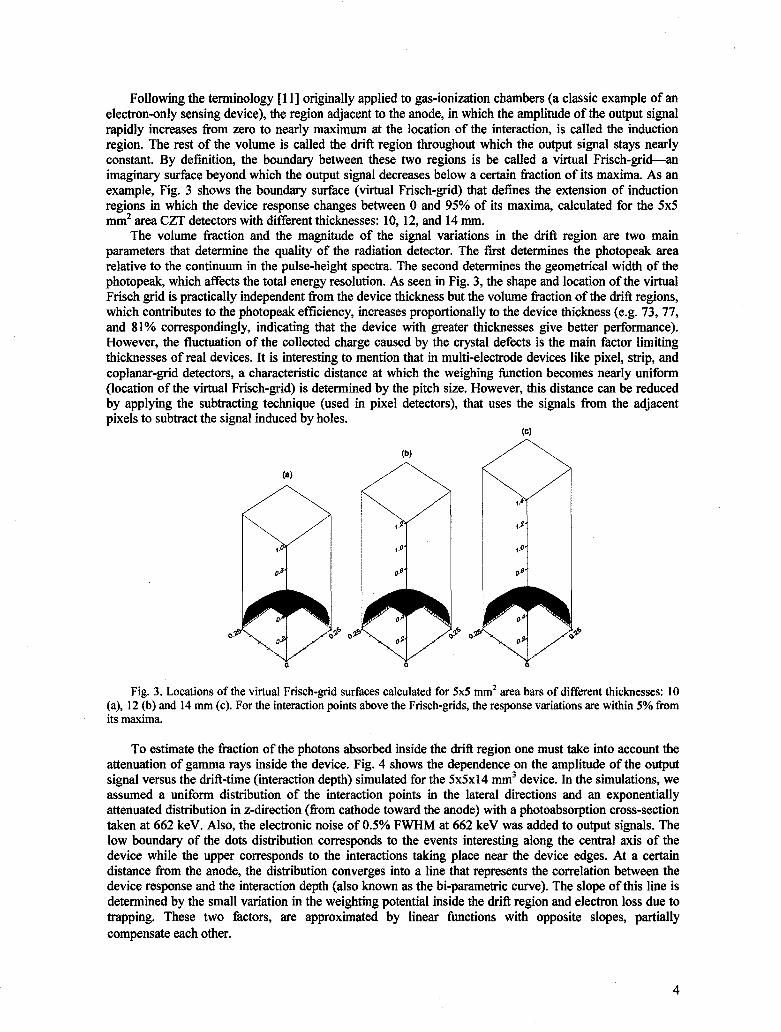
Following the terminology [ 113 originally applied to gas-ionization chambers (a classic example of an electron-only sensing device), the region adjacent to the anode, in which the amplitude of the output signal rapidly increases from zero to nearly maximum at the location of the interaction, is called the induction region. The rest of the volume is called the drift region throughout which the output signal stays nearly constant. By definition, the boundary between these two regions is be called a virtual Frisch-grid-an imaginary surface beyond which the output signal decreases below a certain fraction of its maxima. As an example, Fig. 3 shows the boundary surface (virtual Frisch-grid) that defines the extension of induction regions in which the device response changes between 0 and 95% of its maxima, calculated for the 5x5 mm2 area CZT detectors with different thicknesses: 10, 12, and 14 mm.
The volume fraction and the magnitude of the signal variations in the drift region are two main parameters that determine the quality of the radiation detector. The first determines the photopeak area relative to the continuum in the pulse-height spectra. The second determines the geometrical width of the photopeak, which affects the total energy resolution. As seen in Fig. 3, the shape and location of the virtual Frisch grid is practically independent from the device thickness but the volume fraction of the drift regions, which contributes to the photopeak efficiency, increases proportionally to the device thickness (e.g. 73,77, and 81% correspondingly, indicating that the device with greater thicknesses give better performance). However, the fluctuation of the collected charge caused by the crystal defects is the main factor limiting thicknesses of real devices. It is interesting to mention that in multi-electrode devices like pixel, strip, and coplanar-grid detectors, a characteristic distance at which the weighing function becomes nearly uniform (location of the virtual Frisch-grid) is determined by the pitch size. However, this distance can be reduced by applying the subtracting technique (used in pixel detectors), that uses the signals from the adjacent pixels to subtract the signal induced by holes.
(C)
0 0
Fig. 3. Locations of the virtual Frisch-grid surfaces calculated for 5x5 mm2 area bars of different thicknesses: 10 (a), 12 (b) and 14 mm (c). For the interaction points above the Frisch-grids, the response variations are within 5% from its maxima.
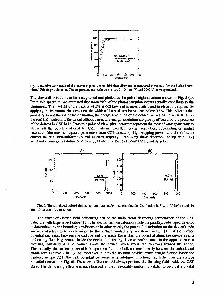
To estimate the fraction of the photons absorbed inside the drift region one must take into account the attenuation of gamma rays inside the device. Fig. 4 shows the dependence on the amplitude of the output signal versus the drift-time (interaction depth) simulated for the 5x5~14 mm3 device. In the simulations, we assumed a uniform distribution of the interaction points in the lateral directions and an exponentially attenuated distribution in z-direction (from cathode toward the anode) with a photoabsorption cross-section taken at 662 keV. Also, the electronic noise of 0.5% FWHM at 662 keV was added to output signals. The low boundary of the dots distribution corresponds to the events interesting along the central axis of the device while the upper corresponds to the interactions taking place near the device edges. At a certain distance from the anode, the distribution converges into a line that represents the correlation between the device response and the interaction depth (also known as the bi-parametric curve). The slope of this line is determined by the small variation in the weighting potential inside the drift region and electron loss due to trapping. These two factors, are approximated by linear hctions with opposite slopes, partially compensate each other.
4
Fig. 4. Relative amplitude of the output signals versus drift-time distribution measured simulated for the 5x5~14 mm3 virtual Frisch-grid detector. The pr-product and cathode bias are 2x10" cm2N and 2000 V, correspondently.
500
400
300
200
100 0
The above distribution can be histogramed and plotted as the pulse-height spectrum shown in Fig. 5 (a). From this spectrum, we estimated that more 90% of the photoabsorption events actually contribute to the photopeak. The FWHM of the peak is -1.5% at 662 keV and is mostly attributed to electron trapping. By applying the bi-parametric correction, the width of the peak can be reduced below 0.5%. This indicates that geometry in not the major factor limiting the energy resolution of the device. As we will discuss latter, in the real CZT detectors, the actual effective area and energy resolution are greatly affected by the presence of the defects in CZT bulk. From this point of view, pixel detectors represent the most advantageous way to utilize all the benefits offered by CZT material: excellent energy resolution, sub-millimeter spatial resolution (the most anticipated parameters from CZT detectors), high stopping power, and the ability to correct material non-uniformities and electron trapping. Employing these detectors, Zhang et a1 [12] achieved an energy resolution of 4 % at 662 keV for a 15x15~10 mm3 CZT pixel detector.
. . . , . . , . . .
150
100 6
50
0:
-
1
- d I -
1.5% : FWHM I
2 L' -
Channels Channels
Fig. 5. The simulated pulse-height spectrum obtained by histograming the distribution in Fig. 4: (a) before and (b) after bi-parametric correction.
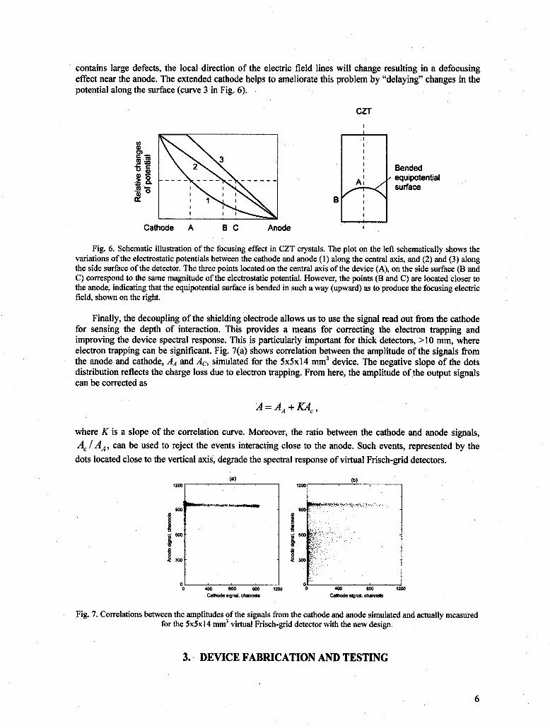
The effect of electric field defocusing can be the main factor degrading performance of the CZT detectors with large aspect ratios [ 101. The electric field distribution inside the parallepiped-shaped detector is determined by the boundary conditions or in other words, the potential distribution on the device's side surfaces which in turn is determined by the surface conductivity. As shown in Ref. [lo], if the surface potential decreases between the cathode and the anode faster than the potential along the device axis, a defocusing field is generated inside the device diminishing detector performance. In the opposite case, a focusing drift-field will be formed inside the device which steers the electrons toward the anode. Theoretically, the surface potential is independent from the bulk changes linearly between the cathode and anode levels (curve 2 in Fig. 6). Moreover, due to the uniform positive space charge formed inside the depleted n-type CZT, the bulk potential decreases as a sub-linear function, i.e., faster than the surface potential (curve 1 in Fig. 6). These two effects should always produce the focusing field inside the CZT slabs. The defocusing effect was not observed in the high-quality uniform crystals, however, if a crystal
5
contains large defects, the local direction of the electric field lines will change resulting in a defocusing effect near the anode. The extended cathode helps to ameliorate this problem by “delaying” changes in the potential along the surface (curve 3 in Fig. 6).
CZT I
Cathode A B C Anode
Bended equipotential surface
Fig. 6. Schematic illustration of the focusing effect in CZT crystals. The plot on the left schematically shows the variations of the electrostatic potentials between the cathode and anode (1) along the central axis, and (2) and (3) along the side surface of the detector. The three points located on the central axis of the device (A), on the side surface (B and C) correspond to the same magnitude of the electrostatic potential. However, the points (B and C) are located closer to the anode, indicating that the equipotential surface is bended in such a way (upward) as to produce the focusing electric field, shown on the right.
Finally, the decoupling of the shielding electrode allows us to use the signal read out from the cathode for sensing the depth of interaction. This provides a means for correcting the electron trapping and improving the device spectral response. This is particularly important for thick detectors, >lo mm, where electron trapping can be significant. Fig. 7(a) shows correlation between the amplitude of the signals from the anode and cathode, AA and Ac, simulated for the 5x5~14 mm3 device. The negative slope of the dots distribution reflects the charge loss due to electron trapping. From here, the amplitude of the output signals can be corrected as
where K is a slope of the correlation curve. Moreover, the ratio between the cathode and anode signals, A, / A , , can be used to reject the events interacting close to the anode. Such events, represented by the dots located close to the vertical axis, degrade the spectral response of virtual Frisch-grid detectors.
Fig. 7. Correlations between the amplitudes of the signals from the cathode and anode simulated and actually measured for the 5x5~14 mm3 virtual Frisch-grid detector with the new design.
3. DEVICE FABRICATION AND TESTING
6
More than 50 ready-to-use parallelepiped-shaped CZT detectors (bars) with dimensions 5x5~10, 5x5~12, and 5x5~14 mm3 and with planar contacts deposited the on top and bottom surfaces were obtained form several vendors. Eventually, these crystals will be assembled in 4x4 detector modules for the handheld gamma-ray imaging cameraunder development at BNL [ 131. The bars were first configured as conventional Frisch-ring detectors by using a Teflon tape and tested as described in Ref. [ 141.
After completing the tests the detectors were disassembled and prefabricated according to a new design. The cathode contacts were “extended” by partially deepening the detectors in a gold chloride solution. Then the detector were encapsulated by used the high dielectric-strength, ultra-thin polyester shr ink tubes, manufactured by Advanced Polymers, Inc. [15]. This method obviates the numerous overlapping layers of Teflon or Kapton required for reliable insulation (Ref [ 141) that make the insulating layer too thick; a thin insulating layer is a critical parameter for achieving the effective shielding in the devices.
The encapsulation process includes two steps. First, the rectangular polyester shells were pre-formed by using an aluminum mandrel and a heat treatment (Fig. 8). Then a detector is inserted inside the shell where the open ends are closed by two aluminum mandrels with small grooves to ensure tight encapsulation near the ends of the crystal. The above assembly is self-supported and self-aligning. Finally, a heating step up to 75-80 C is applied to form a thin seamless encapsulating layer that follows the exact shape of the crystal without damaging the surface or adversely affecting the device’s electrical or mechanical properties. The tube is cut with a razor, and the mandrels are pulled away.
,
Step 1
65-70 C ___)
step 2
Aluminum Preformed CZT mandrd shrink tuba ClYStal
Cut tube here with a razor
\
Pull aluminum 1 mandrels
Fig. 8. Crystal encapsulation steps: (1) pre-form a polyester shrink tube, (2) insert the crystal between two mandrels inside the preformed tube, (3) apply heat, (4) cut with tube with a razor, and (5 ) remove the mandrels.
Two flexible wires were glued to the electrodes with conductive epoxy and secured with a thin layer of RTV adhesive. The fabricated devices were mounted on small substrates with three pin connectors that could be plugged into the PC board of a test box. The anode and cathode signals were read out with the standard eV Products preamplifiers. A negative bias was applied to the cathode while the shielding electrode was grounded. We used standard spectroscopy electronics to generate pulse-height spectra fiom
Am, I3’Cs and %o sources. We also applied digital pulse shape methods and coincidence measurements described elsewhere [16]. In this work, the output signals fiom the preamplifiers were digitized with a 24 1
7
LeCroy 6050 Waverunner. For the coincidence measurements, we employed a small, -3 cm3, BaF2 detector and the 51 1-keV annihilation photons emitted by the 68Ge source to produce signals in the CZT device under the test and BaF2 detector. Fast signals generated by the BaFz detector were used as triggers to locate the interaction moment of an incident photon. X-ray scans were performed to study the device response uniformities as described in Ref. [ 161.
4. RESULTS AND DISCUSSION
The main advantage of the new design is that it provides better shielding efficiency for parallepiped- shaped virtual Frisch-grid detectors. Fig. 9 compares the correlation curves evaluated for a 5x5~14 mm3 CZT bar implementing the new and old designs. In detectors using the new design, the drift regions extend closer to the anode while the shapes of the correlation curve approached the theoretical limits as illustrated in Fig. 10. The solid lines represent the theoretical curves calculated for the central regions for 12 and 14- mm long crystals. In our calculations, we adjusted the p-product to 2.5x10-* cm2N and used 770 cm2Ns for the electron mobility to make a better fit.
Fig. 9. The correlation curves evaluated for detectors using the new and old designs made from the same 5x5~14 mm3 CZT bar. Cathode bias is 2800 V.
Fig. 10. Measured and simulated correlations curves for (a) 5x5~12 and (b) 5x5~14 mm3 virtual Frisch-grid detectors. The ps-product and electron mobility were adjusted to 2.5~10‘~ cm2N and 770 cm2Ns, while the cathode biases were 1500 V and 2000 V for 12 and 14-mm detectors respectively.
On the other hand, if one compares the above curve measured for the 14-mm detector with the simulated distribution shown in Fig. 4, it becomes clear that events interacting near the device edges and near the anode (in the comers) are missing in the measured plots. We believe that the dots representing those events are shifted down to form a wide track of dots that bends toward the beginning of the coordinate system. This fact indicates that the -100-pm insulating layer that separates the shielding electrode from the CZT surface is not sufficiently thin to provide the effective shielding in the comers near the anode. Those events interacting close to the anode that correspond to the bended part of the correlation curve contribute to the low energy tail of the photopeak often seen in the pulse-height spectra. The negative slope of the correlation curve results in a broadening of the peak. Both effects degrade the device spectral
a
response but they can be corrected by using the cathode signal as described in Section 2. As an example, the measured correlation between the cathode and anode signals is shown in Fig. 7(b).
Fig. 1 1 illustrates the application of the correction technique to the 68Ge pulse-height spectrum and the corresponding correlation curve measured for a 5x5~14 mm3 device. The data was evaluated by measuring the waveforms from preamplifiers and applying the pulse-shape analysis described previously. As seen, the low energy tail seen in the original spectrum can also be substantially reduced without losing of photopeak counts by selecting the events with an &/AA ratio greater than 0.005. As a result, the energy resolution improves from 2.8 to 2.1% at 5 1 1 keV for this particular device.
1Mo
wo-
800-
3w-
. I , . I , . .
Raba >O OC5 150 -
loo -
0 0 120 240 360 4M BM) 720 840 884 1080 12W
1
0 -
50 i- 0 sw lOO0 1sw m
I ZOO0
Fig. 11. Pulse-height spectra measured from an uncollimated I3’Cs source with a 14-mm long detector before (top) and after (middle and bottom) correction.
Similarly, Fig. 12 illustrates the application of the correction technique to improve I3’Cs spectrum measured for a 14-mm long device. In principle, the signal read out from the Frisch-ring can be used to substitute for the cathode signal. In this case, the correlation between the anode and sum of the anode and Frisch-ring signals should be used.
9
(a) . . . , _ . . , . . . , . , . .
Before c o d o n 100
80
80
40
20
0 0 300 600 900 1200 ISM)
I Aftetcaredion 'I 80
80
40
20
0 0 s M ) B M g a O l M o
I 1500
Fig. 12. Pulse-height spectra measured from an uncollimated I3'Cs source with a 14-mm long detector before (a) and after (b) correction.
The new design of the virtual Frisch-grid detector should potentially provide an energy resolution better than 0.7% at 662 keV and a large fraction of detected events contributing to the photopeak. This was confirmed with several fabricated devices but not all the fabricated and tested detectors showed such good spectral responses. Unfortunately, for rare exceptions, the performance of real devices is determined by the quality of the CZT material. By testing of more than 50 CZT crystals we confirmed findings by other researchers [17,18] that large-scale crystal defects like twins and dislocations change the local electric field lines distributions and affect charge transport properties of the material. All of these distort the pulse-height spectra by increasing the continuum and reducing a number of the counts under the peak. We also observed the broadening of the photopeaks correlated with the higher concentration and larger size of Te inclusions, seen with transmission IR microscopy. Figs. 13 and 14 illustrate the effects of both the large structural defects and Te inclusions on the performance of thick CZT detectors. Fig. 13 represents the detectors fabricated from a 5x5~12 cm3 crystal that does not have large defects but contains -lo5 cm-3 Te inclusions with dimensions in the range 1-20 pm. As seen, the device exhibits an excellent pulse-height spectrum of I3'Cs with a narrow photopeak, 1.3% FWHM at 662 keV, and low-level continuum. For this detector, a high spatial resolution X-ray map shows a uniform response over the entire area of the device. However, several Te inclusion located near the cathode can be identified as small dark spots on the 2D image and shallow deeps in the 3D plot. Previously, we demonstrated [19,20] that the cumulative effect of such inclusions over the long drift distances can result in the peak broadening and can account for the energy resolution measured for this detector. In contrast, the detector represented in Fig. 14, in addition to Te inclusions, has several large defects that change the local distribution of the electric field lines. Due to the small lateral dimensions of the detector there is a large probability that bended field lines touch or intersect side surfaces of the crystal. As a result, for some regions near the device's edges, the electrons produced by the incident photons will be driven to the surface and are lost due to the surface recombination. In the X-ray maps, such regions are seen as dark areas in the 2D image or "chipped" edges in the 3D image. Because of the significant charge loss, these events do not affect the FWHM of the photopeak but affect the overall shape of the pulse-height spectrum (e.g. increase the continuum in expenditure of the photopeak area). These same events also result in the low energy tail that extends between the photopeak and the Compton edge.
10
Fig. 13. The 13'Cs pulse-height spectrum and 25-keV x-ray maps measured for 5x5~12 mm3 detector without large structural defects. The spatial resolution of the x-ray map is 25x25 pm'.
em
% - rm
0 I rm em r2m ,em zom
Fig.14. The 13'Cs pulse-height spectrum and 25-keV x-ray maps measured for 5x5~10 mm3 detector with large structural defects. The spatial resolution of the x-ray map is 50x50 pm'.
5. CONCLUSION
We evaluated the performance of the basic designs of CZT detectors from the viewpoint of the residual effect of the uncollected holes in CZT detectors.
Although a great variety of the designs have been proposed for CZT and other semiconductor detectors operating in an electron-collection mode, they utilize only two ways for minimizing the effect of the uncollected holes; namely, electrostatically shielding the collecting electrodes from the effect of the hole or electronically subtracting the charge signals induced by the hole. In practice, it is impossible to completely shield (or subtract) the charge induced by the uncollected holes over the device's entire active volume.
In some designs for CZT detectors, the variation of the output signals in the drift region can be corrected while rejecting the interaction events from the induction region (improving the device's preformance). Furthermore, fluctuations of the output signals caused by smooth variations of the electron mobility-lifetime product can be corrected in designs that provide coordinate information on the interaction points.
The device's side surfaces play important role in CZT detectors. The drift-lines can be terminated by the side surfaces before reaching the collecting electrodes resulting in a signal loss for interacting events
11
near the edges. To avoid this effect, the electrostatic potential on the surfaces should decrease more slowly than that in the bulk; this will ensure that the field lines are focused towards the collecting electrodes.
Finally, the efficiency of designs always depends on the boundary conditions. While other conducting electrodes can be placed near the side surfaces and the collecting electrodes, the contacting or non- contacting shielding electrodes must always be sited on the device’s side surfaces to improve the efficiency of shieldinghbtraction.
ACKNOWLEDGEMENTS
This work was supported by U.S. Department of Energy, Office of Nonproliferation Research and Engineering, NA-22. The manuscript has been authored by Brookhaven Science Associates, LLC under Contract No. DE-AC02-98CH1-886 with the U.S. Department of Energy. The United States Government retains, and the publisher, by accepting the article for publication, acknowledges, a world-wide license to publish or reproduce the published form of this manuscript, or allow others to do so, for the United States Government purposes.
REFERENCES
[ 13 NASA Swift Mission, http://www.nasa.gov/missionqages/swift/main/index.html. [2] P. N. Luke, “Single-polarity charge sensing in ionization detectors using coplanar electrodes”, Appl.
Phys. Lett. 65 (22), pp. 2884-2886, 1995. Also see US Patent 5,530,249 by P. N. Luke (1996). [3] K. Parnham, C. Szeles, K.G. Lynn, R. Tjossem, “Performance Improvement of CdZnTe Detectors
Using Modified Two-Terminal Electrode Geometry,” accepted for publication in Hard x-ray, Gamma- Ray and Neutron Detector Physics, Proceedings of SPIE, 1999.
[4] Ritec, Inc., Riga, Latvia, http://www.ritec.lv/HtmVpub.html. [5] Csaba Szeles, Derek Bale, Joseph Grosholz, Jr., Gary L. Smith, Michael Blostein, and John Eger,
“Fabrication of High Performance CdZnTe Quasi-Hemispherical Gamma-ray CAPtureTM Plus Detectors”, Hard X-Ray and Gamma-Ray Detector Physics VIII, edited by Larry A. Franks, Arnold Burger, and Ralph B. James, Proceedings of SPIE Vol. 63 19 (SPIE, Bellingham, WAY 2006).
[6] D.S. McGregor and R.A. Rojeski, U.S. Patent 6,175,120. [7] G. Montemont, M. Arques, L. Verger, and J. Rustique, “A Capacitive Frisch Grid Structure for
[SI H. H. Barrett, J. D. Eskin, and H. B. Barber, Phys. Rev. Lett. 75 (l), p. 156,1995. [9] A. Kargar, A.M. Jones, W.J. McNeil, and D.S. McGregor, “CdZnTe Frisch Ring Detectors for Low-
Energy Gamma Ray Spectroscopy,” Nuclear Instruments and Methods, A558 (2006) pp. 487-503. [10]A. E. Bolotnikov, G. S. Camarda, G. A. Carini, M. Fiederle, L. Li, D. S. McGregor, W. McNeil, G. W.
Wright, R. B. James, “Performance Characteristics of Frisch-Ring CdZnTe Detectors”, IEEE Trans. Nucl. Sci., vol. 53 (2), pp. 607-614,2006.
[ 1 11 0. Buneman, T.E. Cranshaw, and J.A. Harvey, “Design of Grid Ionization Chambers,” Can. J Res.,
[12]F. Zhang, Z. He, D. Xu, G. F. Knoll, D. K. Wehe, and J. E. Berry, “Improved resolution for 3D position sensitive CdZnTe spectrometers,” IEEE Trans. Nucl. Sci., Vol. 5 1, pp. 2427-243 1,2004.
[13]Y. Cui, A. E. Bolotnikov, G. S. Camarda, G. A. Carini, G. De Geronimo, P. O’Connor, R. B. James, A. Kargar, M. J. Harrison, and D. S. McGregor, “Readout System for Arrays of Frisch-Ring CdZnTe Detectors”, IEEE Transactions on Nuclear Science, in press, August, 2007.
[14]A. E. Bolotnikov, G. S. Camarda, G. A. Carini, G. W. Wright, R. B. James, D.S. McGregor, W. McNeil, “New Results from Performance Studies of Frisch-Grid CdZnTe Detectors”, SPIE, 5540, pp.
CdZnTe Detectors”,IEEE Trans. Nucl. Sci., Vol. 48, pp. 278-281,2001.
A27 (1949) pp. 191-206.
33-45,2004. [ 151 Advanced Polymers, Inc., Salem, NH 03079, http://www.advpoly.com [ 161 A. E. Bolotnikov, G. S. Camarda, G. A. Carini, M. Fiederle, L. Li, G. W. Wright, and R. B. James, “Performance Studies of
CdZnTe Detector by Using a Pulse-Shape Analysis”, in Proceedings of SPIE Hard X-Ray and Gamma-Ray Detector Physics VII, edited by R. B. James, L. A. Franks, and A. Burger (SPIE, Bellingham, WA, 2005), 592OOK-1- 59200K-12.
12
[17]B. H. Parker, C. M. Stahle, D. Roth, S. Babu, J. Tueller, “Effect of twin boundaries on the spectroscopic performance of CdZnTe detectors,” in Hard X-Ray and Gamma-Ray Detector Physics 111, R. James ed., Proc. SPIE 4508, p. 68-78,2001.
[18]S. A. Soldner, A. J. Narvett, D. E. Covalt, and C. Szeles, “Characterization of the charge transport uniformity of CdZnTe crystals for large-volume nuclear detector applications, ZEEE Trans. Nucl. Sci., Vol. 51, n. 5pp. 2443-2447,2004.
[19]A. E, Bolotnikov, G. S. Camarda, G. A. Carini, Y, Cui, L. Li and R. B. James, “Cumulative Effects of Te Precipitates in CdZnTe Radiation Detectors”, Nucl. Instruments and Methods A571, 687-698 (2007).
[20] G. S. Camarda, A. E. Bolotnikov, Y. Cui, K. T. Kohman, and R. B. James, “CdZnTe room-temperature semiconductor gamma-ray detector for national-security applications”, IEEE Trans. on Nuclear Science, submitted.