Page 1
CMOSedu.com Nano Memory Module – by R. Jacob Baker
IEEE SSCS Lehigh/Princeton/Columbia Chapters Present
Distinguished Lecture Colloquia, October 2014
R. Jacob Baker
[email protected]
Overview: This work proposes a novel DRAM module and interconnect architectures in an
attempt to improve computing energy use and performance. A low cost advanced packaging
technology is used to propose an 8 die and 32-die memory module. The 32-die memory module
measures less than 2 cm3. The size and packaging technique allow the memory module to consume
less power than conventional module designs. A 4 Gb DRAM architecture utilizing 64 data pins is
proposed. The DRAM architecture is inline with ITRS roadmaps and can consume 50% less power
while increasing bandwidth by 100%. The large number of data pins are supported by a low power
capacitive-coupled interconnect. The receivers developed for the capacitive interface were
fabricated in 0.5 µm and 65 nm CMOS technologies. The 0.5 µm design operated at 200 Mbps,
used a coupling capacitor of 100 fF, and consumed less than 3 pJ/bit of energy. The 65 nm design
operated at 4 Gbps, used a coupling capacitor of 15 fF, and consumed less than 15 fJ/bit and order
of magnitude smaller consumptions than previously reported receiver designs.
Low-Power, High-Bandwidth, and Ultra-Small
Memory Module Design
1
Page 2
CMOSedu.com Nano Memory Module – by R. Jacob Baker
IEEE SSCS Lehigh/Princeton/Columbia Chapters Present
Distinguished Lecture Colloquia, October 2014
Why is Power Such a Big Deal? • Let’s say that at any given time there are, at least,
1,000,000 people playing World of Warcraft (WoW, a
very reasonable assumption)
• Further let’s say that the power consumed by each of
these players for: processor, memory (DRAM), computer
fan, hard disk drive, monitor(s), modem, remote servers,
communication channels (e.g., satellites links), cooling,
etc. is 1000 Watts (again a very reasonable assumption)
• More than 1 GW of power is needed at any time for
people to play WoW. This is the amount of power
generated by a small nuclear power plant!
Page 3
CMOSedu.com Nano Memory Module – by R. Jacob Baker
IEEE SSCS Lehigh/Princeton/Columbia Chapters Present
Distinguished Lecture Colloquia, October 2014
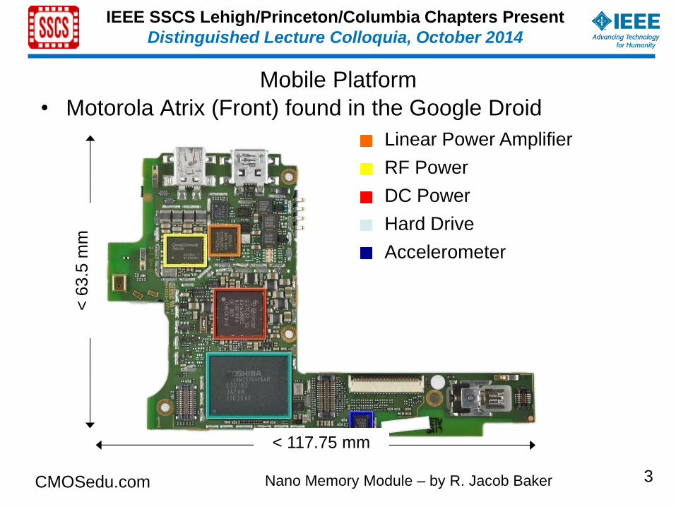
Mobile Platform
• Motorola Atrix (Front) found in the Google Droid
< 117.75 mm
< 6
3.5
mm
Linear Power Amplifier
RF Power
Management DC Power
Management Hard Drive
Accelerometer
3
Page 4
CMOSedu.com Nano Memory Module – by R. Jacob Baker
IEEE SSCS Lehigh/Princeton/Columbia Chapters Present
Distinguished Lecture Colloquia, October 2014
Mobile Platform
• Motorola Atrix (Back)
Memory (DSP)
Memory & CPU
HSPA+ DSP
802.11n & Bluetooth
Compass
4
Page 5
CMOSedu.com Nano Memory Module – by R. Jacob Baker
IEEE SSCS Lehigh/Princeton/Columbia Chapters Present
Distinguished Lecture Colloquia, October 2014
Server Platform • Intel Server Board S5502UR
Memory Slots
5
Page 6
CMOSedu.com Nano Memory Module – by R. Jacob Baker
IEEE SSCS Lehigh/Princeton/Columbia Chapters Present
Distinguished Lecture Colloquia, October 2014
Organization
• Main Memory Limitations
• Nano-Module
• Wide I/O DRAM Architecture
• High Bandwidth Interconnect
• Hybrid Memory Cube
6
Page 7
CMOSedu.com Nano Memory Module – by R. Jacob Baker
IEEE SSCS Lehigh/Princeton/Columbia Chapters Present
Distinguished Lecture Colloquia, October 2014
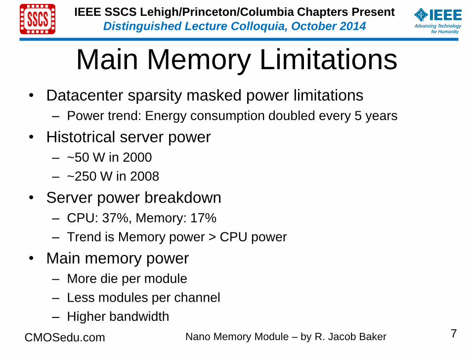
Main Memory Limitations • Datacenter sparsity masked power limitations
– Power trend: Energy consumption doubled every 5 years
• Histotrical server power
– ~50 W in 2000
– ~250 W in 2008
• Server power breakdown
– CPU: 37%, Memory: 17%
– Trend is Memory power > CPU power
• Main memory power
– More die per module
– Less modules per channel
– Higher bandwidth
7
Page 8
CMOSedu.com Nano Memory Module – by R. Jacob Baker
IEEE SSCS Lehigh/Princeton/Columbia Chapters Present
Distinguished Lecture Colloquia, October 2014
Main Memory Limitations
8
Page 9
CMOSedu.com Nano Memory Module – by R. Jacob Baker
IEEE SSCS Lehigh/Princeton/Columbia Chapters Present
Distinguished Lecture Colloquia, October 2014
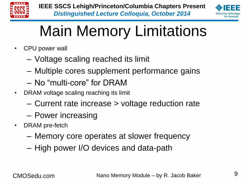
Main Memory Limitations • CPU power wall
– Voltage scaling reached its limit
– Multiple cores supplement performance gains
– No “multi-core” for DRAM • DRAM voltage scaling reaching its limit
– Current rate increase > voltage reduction rate
– Power increasing • DRAM pre-fetch
– Memory core operates at slower frequency
– High power I/O devices and data-path
9
Page 10
CMOSedu.com Nano Memory Module – by R. Jacob Baker
IEEE SSCS Lehigh/Princeton/Columbia Chapters Present
Distinguished Lecture Colloquia, October 2014
Main Memory Limitations
10
Page 11
CMOSedu.com Nano Memory Module – by R. Jacob Baker
IEEE SSCS Lehigh/Princeton/Columbia Chapters Present
Distinguished Lecture Colloquia, October 2014
Main Memory Limitations • DRAM inefficiencies increase cost and power
– Processor cache increasing
– Intel Nehalem processor
– DRAM would need to have L3 BW and latency
– “…create the illusion of a large memory that we can access as
fast as a very small memory.” – Patterson & Hennessy
Local L1 L2 L3 RAM
Read BW [GB/s] 45.6 31.1 26.2 10.1
Write BW [GB/s] 45.6 28.8 19.9 8.4
Latency [ns]
(cycles)
1.3 (4) 3.4 (10) 13.0 (38) 65.1
(191)
11
Page 12
CMOSedu.com Nano Memory Module – by R. Jacob Baker
IEEE SSCS Lehigh/Princeton/Columbia Chapters Present
Distinguished Lecture Colloquia, October 2014
Main Memory Limitations • DRAM efficiencies increase performance
• Capacity versus Performance
• Capacity costs power
– Multiple memory channels
– Each additional module increases power
12
Page 13
CMOSedu.com Nano Memory Module – by R. Jacob Baker
IEEE SSCS Lehigh/Princeton/Columbia Chapters Present
Distinguished Lecture Colloquia, October 2014
Main Memory Limitations • Bandwidth versus performance
• Bandwidth costs power
– Buffer on board
– Multiple channels
13
Page 14
CMOSedu.com Nano Memory Module – by R. Jacob Baker
IEEE SSCS Lehigh/Princeton/Columbia Chapters Present
Distinguished Lecture Colloquia, October 2014
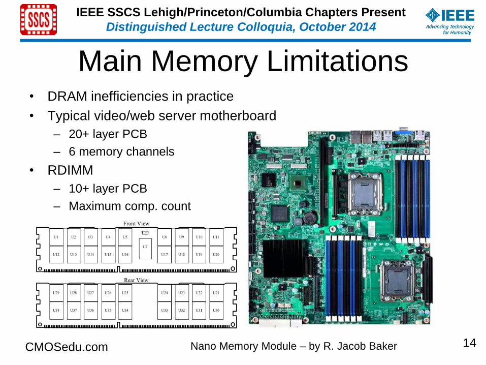
Main Memory Limitations • DRAM inefficiencies in practice
• Typical video/web server motherboard
– 20+ layer PCB
– 6 memory channels
• RDIMM
– 10+ layer PCB
– Maximum comp. count
14
Page 15
CMOSedu.com Nano Memory Module – by R. Jacob Baker
IEEE SSCS Lehigh/Princeton/Columbia Chapters Present
Distinguished Lecture Colloquia, October 2014
Main Memory Limitations • 12 RDIMM
– Termination
• 36 components per DIMM
• 8 I/O per component
• 2.7 W of termination power for a read/write per module
• 32.4 W total termination power
– Wordline firing
• 100 ns activation rate
• 8126 page size
• 200 fF per bitline
• 11.2 W total bitline sense amplifier power
• Sustaining performance gains through capacity and bandwidth
increases power and cost – innovation required.
15
Page 16
CMOSedu.com Nano Memory Module – by R. Jacob Baker
IEEE SSCS Lehigh/Princeton/Columbia Chapters Present
Distinguished Lecture Colloquia, October 2014
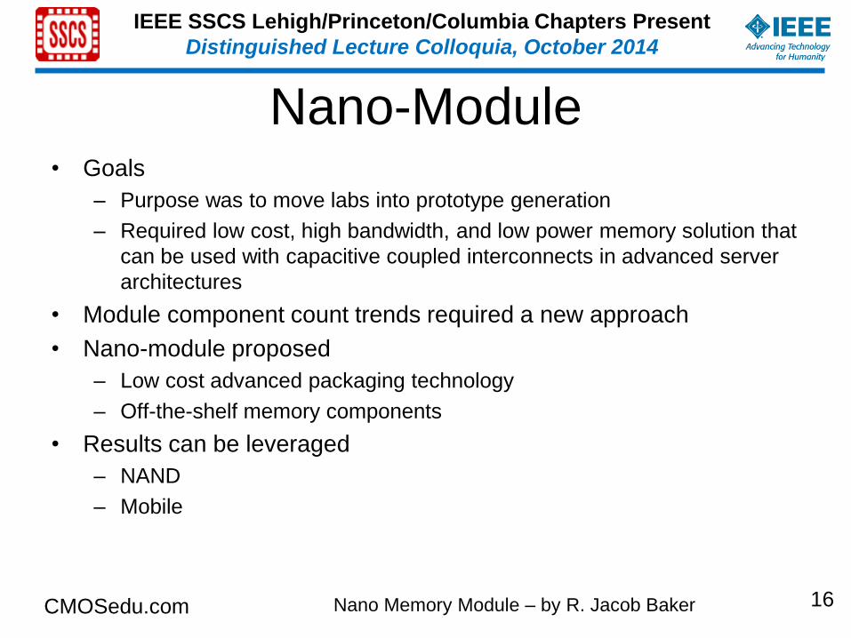
Nano-Module • Goals
– Purpose was to move labs into prototype generation
– Required low cost, high bandwidth, and low power memory solution that
can be used with capacitive coupled interconnects in advanced server
architectures
• Module component count trends required a new approach
• Nano-module proposed
– Low cost advanced packaging technology
– Off-the-shelf memory components
• Results can be leveraged
– NAND
– Mobile
16
Page 17
CMOSedu.com Nano Memory Module – by R. Jacob Baker
IEEE SSCS Lehigh/Princeton/Columbia Chapters Present
Distinguished Lecture Colloquia, October 2014
Nano-Module • Literature review of high capacity memory stacks
• 1990’s
– Multichip Modules
• Realized planar space limitations
– Val & Lemione
– Irvine Sensors
• Solutions proposed in research
– No industry due to memory hierarchy effectiveness
17
Page 18
CMOSedu.com Nano Memory Module – by R. Jacob Baker
IEEE SSCS Lehigh/Princeton/Columbia Chapters Present
Distinguished Lecture Colloquia, October 2014
Nano-Module • Memory stack technology gaining new attention
• Proposed in 2010 (more later about developments)
– Samsung quad die with TSV
• 80 µm pitch, 30 µm diameter, 300 TSV
• RTSV = 5 Ω, CTSV = 300 fF
• Pros:
– Lower power, higher bandwidth
• Cons:
– Cost, integration
PCB Primary Chip
Secondary Chips
TSV (~300)
Rank 0
Rank 1
Rank 2
Rank 3
DRAM Core
DRAM Core
DRAM Core
DRAM Core
RD/WR I/O PAD
Core Test Logic
Core Test Logic
Core Test Logic
18
Page 19
CMOSedu.com Nano Memory Module – by R. Jacob Baker
IEEE SSCS Lehigh/Princeton/Columbia Chapters Present
Distinguished Lecture Colloquia, October 2014
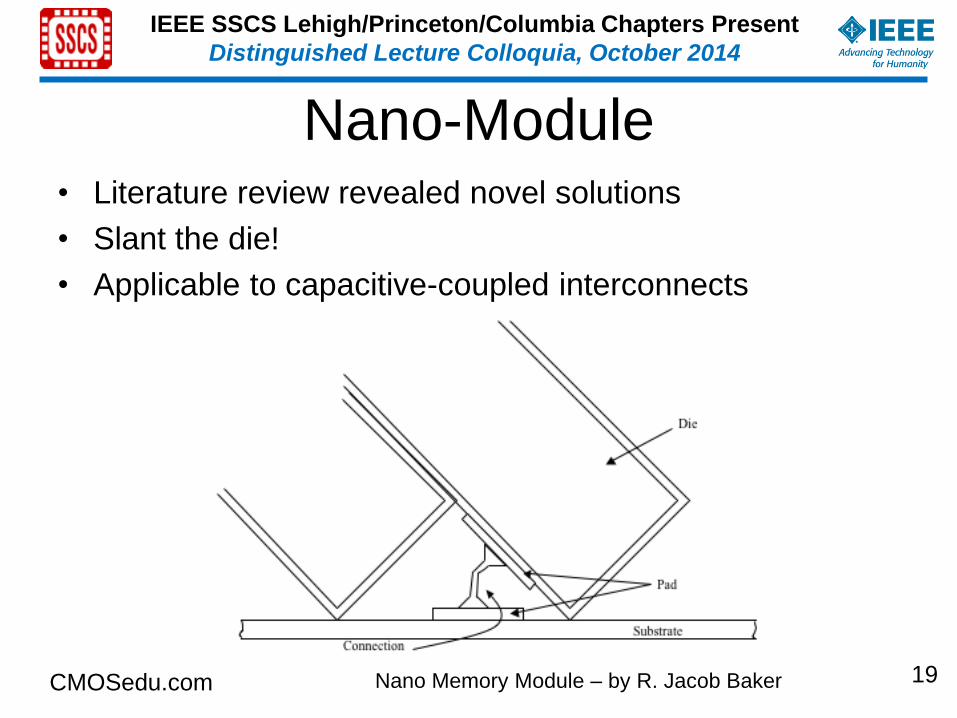
Nano-Module • Literature review revealed novel solutions
• Slant the die!
• Applicable to capacitive-coupled interconnects
19
Page 20
CMOSedu.com Nano Memory Module – by R. Jacob Baker
IEEE SSCS Lehigh/Princeton/Columbia Chapters Present
Distinguished Lecture Colloquia, October 2014
Nano-Module • Not the first to try it:
20
Page 21
CMOSedu.com Nano Memory Module – by R. Jacob Baker
IEEE SSCS Lehigh/Princeton/Columbia Chapters Present
Distinguished Lecture Colloquia, October 2014
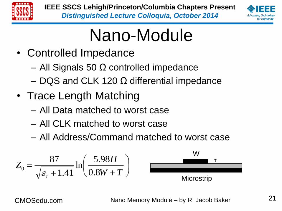
Nano-Module • Controlled Impedance
– All Signals 50 Ω controlled impedance
– DQS and CLK 120 Ω differential impedance
• Trace Length Matching
– All Data matched to worst case
– All CLK matched to worst case
– All Address/Command matched to worst case
TW
HZ
r8.0
98.5ln
41.1
870
W T
Microstrip
21
Page 22
CMOSedu.com Nano Memory Module – by R. Jacob Baker
IEEE SSCS Lehigh/Princeton/Columbia Chapters Present
Distinguished Lecture Colloquia, October 2014
Nano-Module • Size calculations
22
Page 23
CMOSedu.com Nano Memory Module – by R. Jacob Baker
IEEE SSCS Lehigh/Princeton/Columbia Chapters Present
Distinguished Lecture Colloquia, October 2014
Nano-Module • Thermal option
– Thermal conductivity • Silicon, Metals >> Mold Compound
• Hot spots
• Temperature gradient
23
Page 24
CMOSedu.com Nano Memory Module – by R. Jacob Baker
IEEE SSCS Lehigh/Princeton/Columbia Chapters Present
Distinguished Lecture Colloquia, October 2014
Nano-Module
• Thermal option
– Heat plate
24
Page 25
CMOSedu.com Nano Memory Module – by R. Jacob Baker
IEEE SSCS Lehigh/Princeton/Columbia Chapters Present
Distinguished Lecture Colloquia, October 2014
Wide I/O DRAM Architecture • 4 Gb DRAM
– Meets ITRS predictions
• Edge aligned pads
• Page size reduction
• Low cost process
– < 4 levels of metal
– No impact to die size
– No impact to array efficiency
• Move to 64 data pins
– Report challenges
– Propose innovations
25
Page 26
CMOSedu.com Nano Memory Module – by R. Jacob Baker
IEEE SSCS Lehigh/Princeton/Columbia Chapters Present
Distinguished Lecture Colloquia, October 2014
Wide I/O DRAM Architecture • 4 Gb Edge DRAM
– Centralized Row and Column
– Smaller die
– Higher efficiency
– < 4 levels of metal
26
Page 27
CMOSedu.com Nano Memory Module – by R. Jacob Baker
IEEE SSCS Lehigh/Princeton/Columbia Chapters Present
Distinguished Lecture Colloquia, October 2014
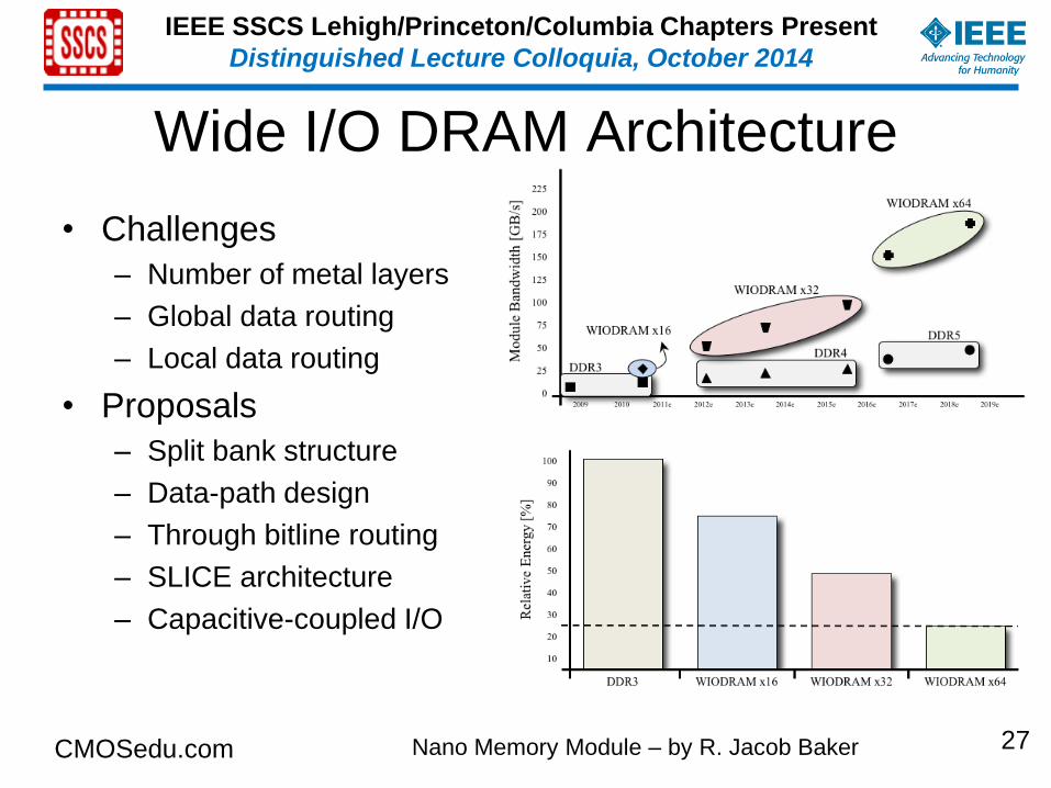
Wide I/O DRAM Architecture
• Challenges
– Number of metal layers
– Global data routing
– Local data routing
• Proposals
– Split bank structure
– Data-path design
– Through bitline routing
– SLICE architecture
– Capacitive-coupled I/O
27
Page 28
CMOSedu.com Nano Memory Module – by R. Jacob Baker
IEEE SSCS Lehigh/Princeton/Columbia Chapters Present
Distinguished Lecture Colloquia, October 2014
High Bandwidth Interconnect • Capacitive-coupling
– Increased bandwidth • Reduced ESD capacitance
• Smaller I/O channel = more I/O
• Removal of inductive channel
– Low power • Reduced ESD capacitance
• Low power Tx & Rx
– Low cost • Simple
– Alignment required
• Literature review – Revealed inefficiencies and lack of
application
28
Page 29
CMOSedu.com Nano Memory Module – by R. Jacob Baker
IEEE SSCS Lehigh/Princeton/Columbia Chapters Present
Distinguished Lecture Colloquia, October 2014
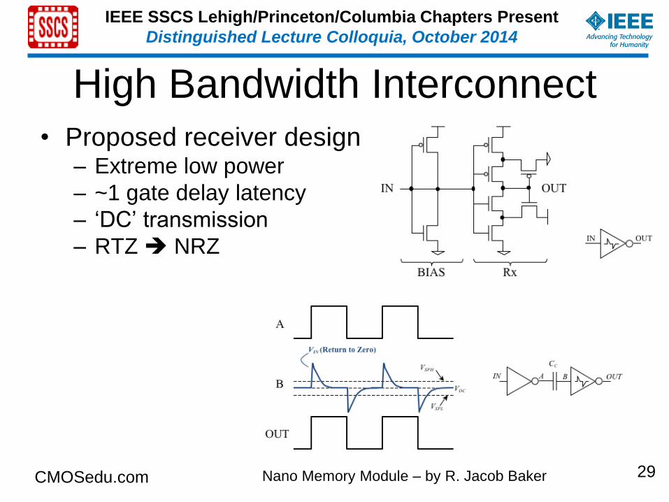
High Bandwidth Interconnect • Proposed receiver design
– Extreme low power
– ~1 gate delay latency
– ‘DC’ transmission
– RTZ NRZ
29
Page 30
CMOSedu.com Nano Memory Module – by R. Jacob Baker
IEEE SSCS Lehigh/Princeton/Columbia Chapters Present
Distinguished Lecture Colloquia, October 2014
High Bandwidth Interconnect 0.5 µm CMOS design (proof
of concept)
5.0 V process
50 fF poly-poly capacitor
200 Mbps
3 – 8 pJ/bit
325 Gb/mm2
30
Page 31
CMOSedu.com Nano Memory Module – by R. Jacob Baker
IEEE SSCS Lehigh/Princeton/Columbia Chapters Present
Distinguished Lecture Colloquia, October 2014
High Bandwidth Interconnect
• Chip micrograph – 1.5 mm x 1.5 mm
– 9 structures
• Experimental results – Operate at VTX = 2.0 V
– 3 pJ/bit at 200 Mbps
Output CC = 100 fF, VTX = 2.0 V
Input
31
Page 32
CMOSedu.com Nano Memory Module – by R. Jacob Baker
IEEE SSCS Lehigh/Princeton/Columbia Chapters Present
Distinguished Lecture Colloquia, October 2014
High Bandwidth Interconnect • 65 nm CMOS
design (proof of
scalability) – 1.2 V process
– 15 fF metal-metal
capacitor
– 4 Gbps
– 17 µm2
– 227 Tbps/mm2
32
Page 33
CMOSedu.com Nano Memory Module – by R. Jacob Baker
IEEE SSCS Lehigh/Princeton/Columbia Chapters Present
Distinguished Lecture Colloquia, October 2014
High Bandwidth Interconnect • Die micrograph
– 2 mm x 2 mm
• Experimental results – 2 Gbps @ 0.9V
– 50 fF coupling capacitor
2.0 Gbps – 0.9 V 1.0 Gbps – 1.2 V
33
Page 34
CMOSedu.com Nano Memory Module – by R. Jacob Baker
IEEE SSCS Lehigh/Princeton/Columbia Chapters Present
Distinguished Lecture Colloquia, October 2014
High Bandwidth Interconnect
34
Page 35
CMOSedu.com Nano Memory Module – by R. Jacob Baker
IEEE SSCS Lehigh/Princeton/Columbia Chapters Present
Distinguished Lecture Colloquia, October 2014
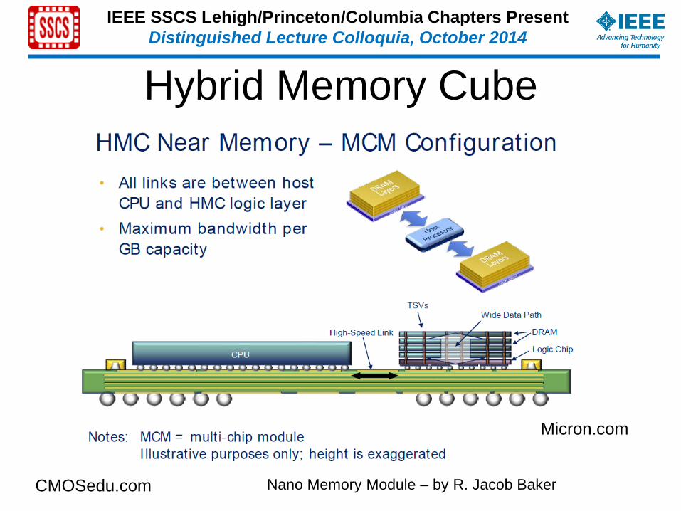
So What is the Industry Moving Towards?
• Hybrid Memory Cube
Micron.com
Page 36
CMOSedu.com Nano Memory Module – by R. Jacob Baker
IEEE SSCS Lehigh/Princeton/Columbia Chapters Present
Distinguished Lecture Colloquia, October 2014
Hybrid Memory Cube
Micron.com
Page 37
CMOSedu.com Nano Memory Module – by R. Jacob Baker
IEEE SSCS Lehigh/Princeton/Columbia Chapters Present
Distinguished Lecture Colloquia, October 2014
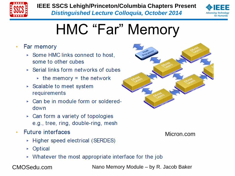
HMC “Far” Memory
Micron.com
Page 38
CMOSedu.com Nano Memory Module – by R. Jacob Baker
IEEE SSCS Lehigh/Princeton/Columbia Chapters Present
Distinguished Lecture Colloquia, October 2014
Micron.com
Page 39
CMOSedu.com Nano Memory Module – by R. Jacob Baker
IEEE SSCS Lehigh/Princeton/Columbia Chapters Present
Distinguished Lecture Colloquia, October 2014
Conclusions • Nano-Module
– Developed a new research direction for industry research
labs
– Developed initial motivation
– Developed initial prototype
• DRAM Architecture
– Demonstrated benefits of wide I/O topologies
– Proposed several low power innovations
– Provided application for novel interconnect technologies
• Capacitive-Coupled Receiver
– Demonstrated low power receiver designs
– Achieved 2 Gbps at < 15 fJ/bit in 65 nm
• Summarized industry direction – Hybrid Memory Cube
39
Page 40
CMOSedu.com Nano Memory Module – by R. Jacob Baker
IEEE SSCS Lehigh/Princeton/Columbia Chapters Present
Distinguished Lecture Colloquia, October 2014
Questions
?
40
Page 41
CMOSedu.com Nano Memory Module – by R. Jacob Baker
IEEE SSCS Lehigh/Princeton/Columbia Chapters Present
Distinguished Lecture Colloquia, October 2014
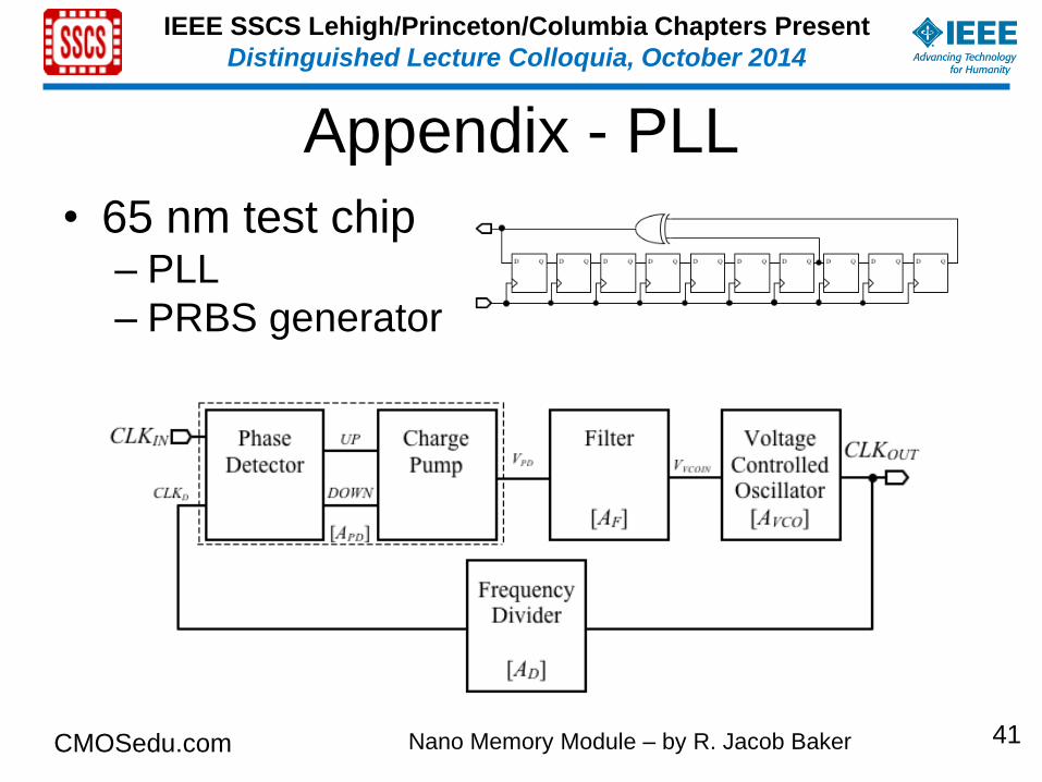
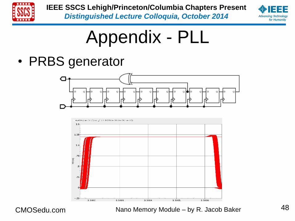
Appendix - PLL
• 65 nm test chip – PLL
– PRBS generator
41
Page 42
CMOSedu.com Nano Memory Module – by R. Jacob Baker
IEEE SSCS Lehigh/Princeton/Columbia Chapters Present
Distinguished Lecture Colloquia, October 2014
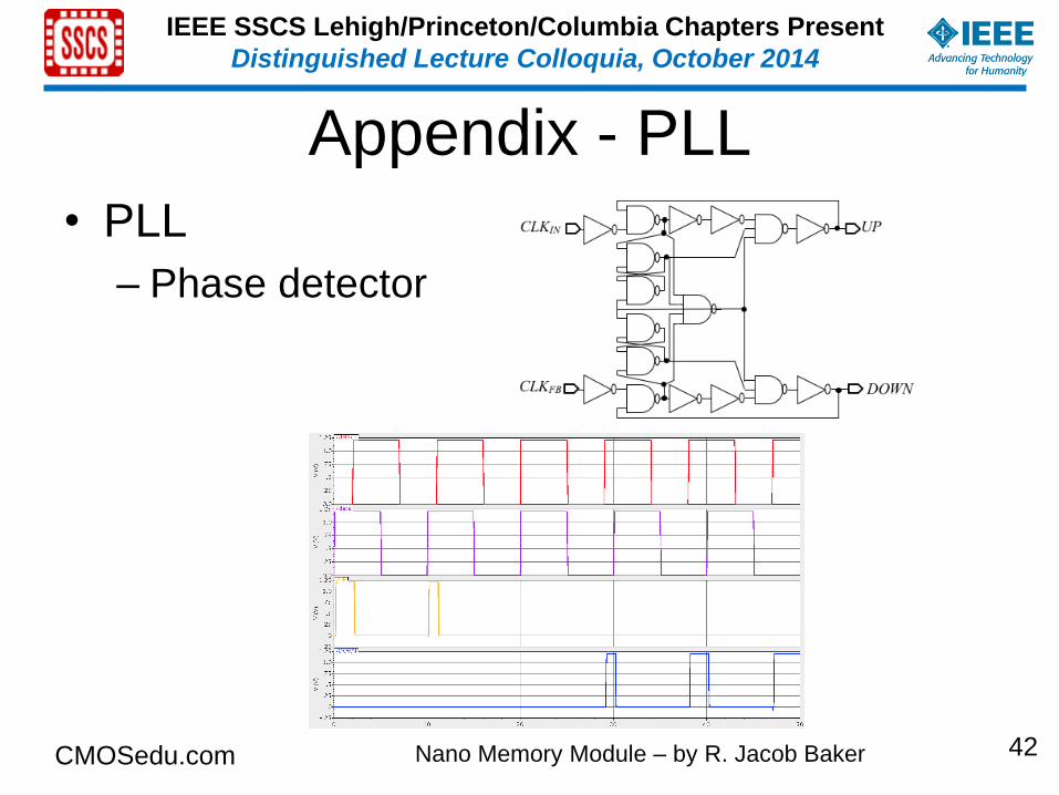
Appendix - PLL
• PLL
– Phase detector
42
Page 43
CMOSedu.com Nano Memory Module – by R. Jacob Baker
IEEE SSCS Lehigh/Princeton/Columbia Chapters Present
Distinguished Lecture Colloquia, October 2014
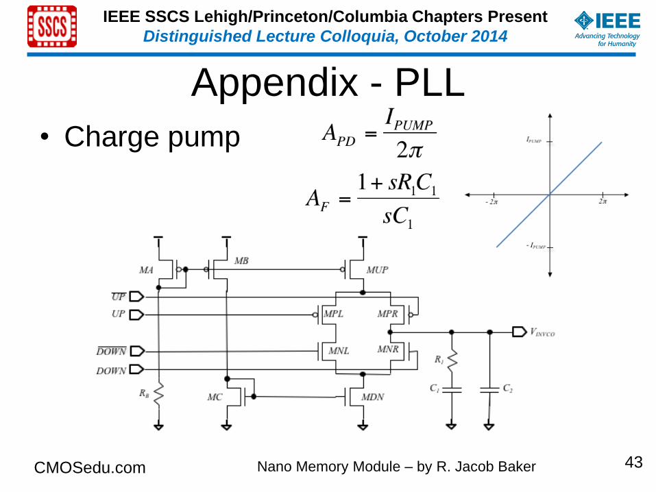
Appendix - PLL
• Charge pump
43
Page 44
CMOSedu.com Nano Memory Module – by R. Jacob Baker
IEEE SSCS Lehigh/Princeton/Columbia Chapters Present
Distinguished Lecture Colloquia, October 2014
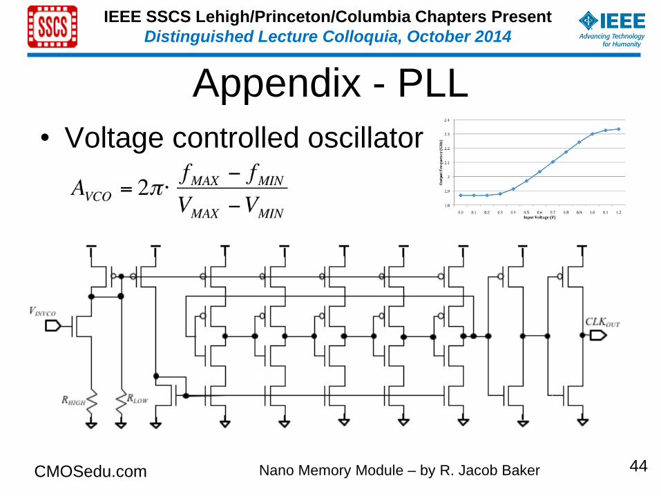
Appendix - PLL
• Voltage controlled oscillator
44
Page 45
CMOSedu.com Nano Memory Module – by R. Jacob Baker
IEEE SSCS Lehigh/Princeton/Columbia Chapters Present
Distinguished Lecture Colloquia, October 2014
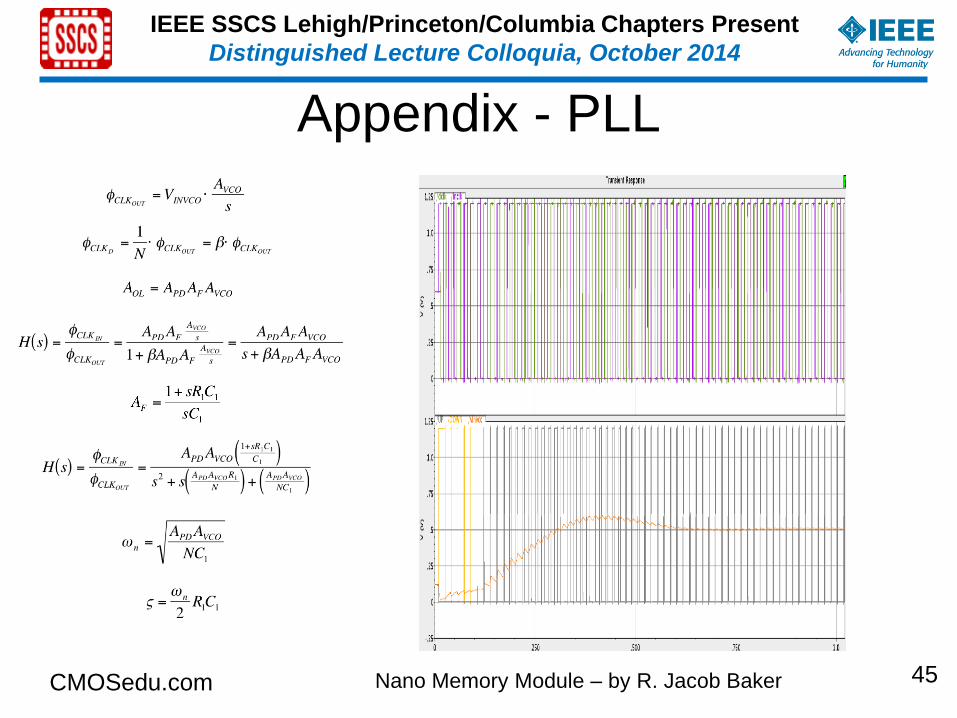
Appendix - PLL
45
Page 46
CMOSedu.com Nano Memory Module – by R. Jacob Baker
IEEE SSCS Lehigh/Princeton/Columbia Chapters Present
Distinguished Lecture Colloquia, October 2014
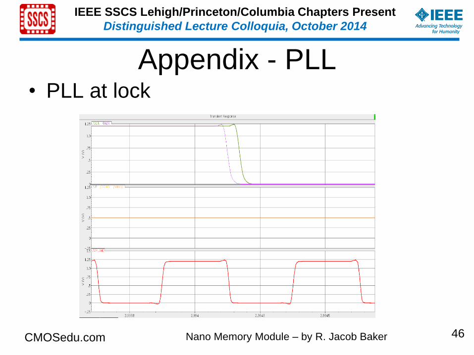
Appendix - PLL • PLL at lock
46
Page 47
CMOSedu.com Nano Memory Module – by R. Jacob Baker
IEEE SSCS Lehigh/Princeton/Columbia Chapters Present
Distinguished Lecture Colloquia, October 2014
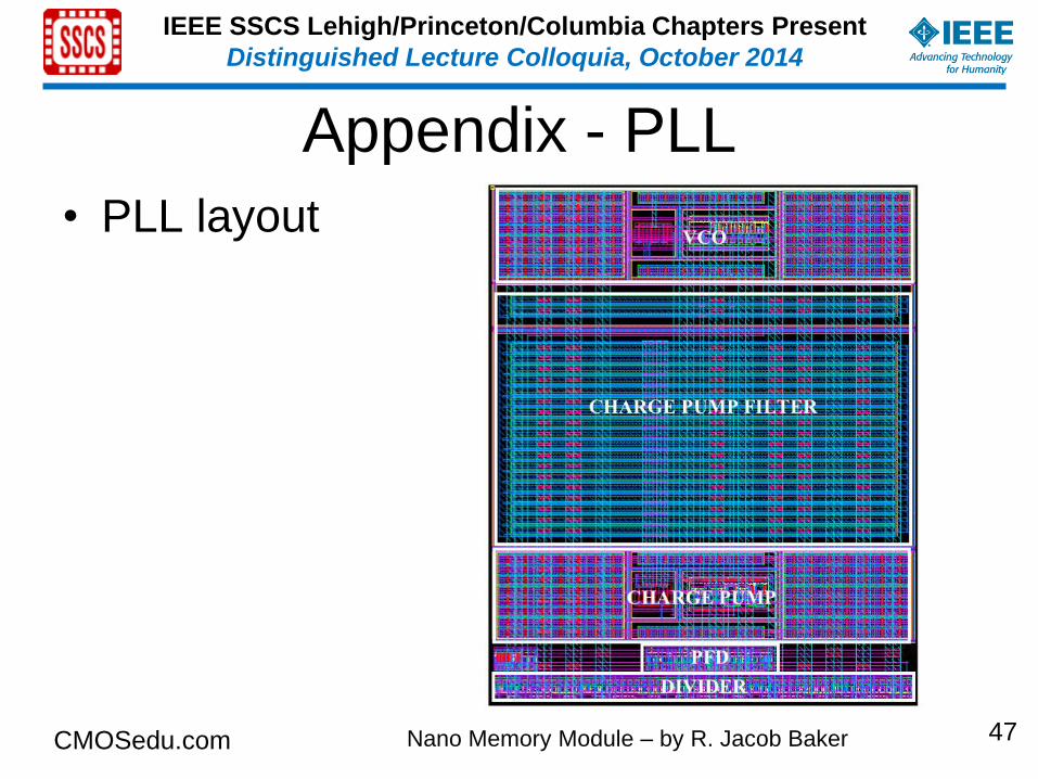
Appendix - PLL
• PLL layout
47
Page 48
CMOSedu.com Nano Memory Module – by R. Jacob Baker
IEEE SSCS Lehigh/Princeton/Columbia Chapters Present
Distinguished Lecture Colloquia, October 2014
Appendix - PLL
• PRBS generator
48
Page 49
CMOSedu.com Nano Memory Module – by R. Jacob Baker
IEEE SSCS Lehigh/Princeton/Columbia Chapters Present
Distinguished Lecture Colloquia, October 2014
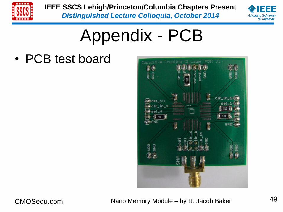
Appendix - PCB
• PCB test board
49
Page 50
CMOSedu.com Nano Memory Module – by R. Jacob Baker
IEEE SSCS Lehigh/Princeton/Columbia Chapters Present
Distinguished Lecture Colloquia, October 2014
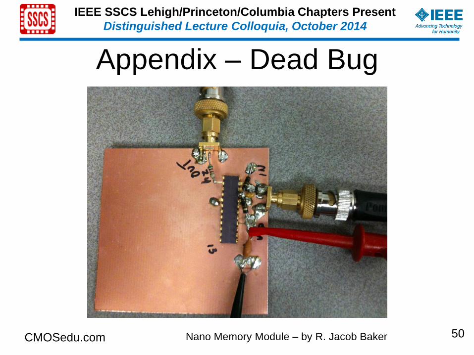
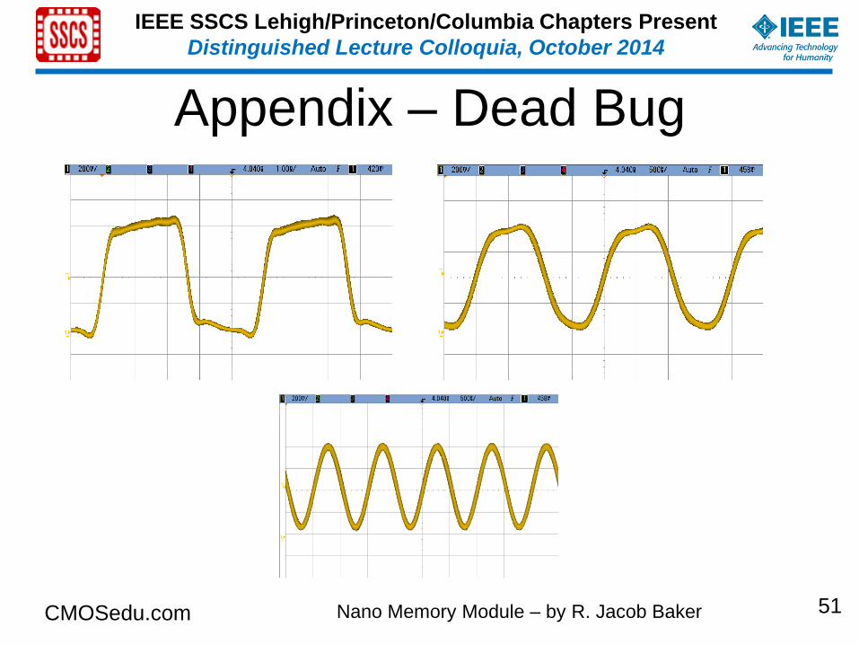
Appendix – Dead Bug
50
Page 51
CMOSedu.com Nano Memory Module – by R. Jacob Baker
IEEE SSCS Lehigh/Princeton/Columbia Chapters Present
Distinguished Lecture Colloquia, October 2014
Appendix – Dead Bug
51
Page 52
CMOSedu.com Nano Memory Module – by R. Jacob Baker
IEEE SSCS Lehigh/Princeton/Columbia Chapters Present
Distinguished Lecture Colloquia, October 2014
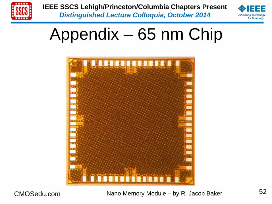
Appendix – 65 nm Chip
52
Page 53
CMOSedu.com Nano Memory Module – by R. Jacob Baker
IEEE SSCS Lehigh/Princeton/Columbia Chapters Present
Distinguished Lecture Colloquia, October 2014
References [1] Val, C.; Lemoine, T.; , "3-D interconnection for ultra-dense multichip modules," Components, Hybrids, and Manufacturing
Technology, IEEE Transactions on , vol.13, no.4, pp.814-821, Dec 1990
[2] Bertin, C.L.; Perlman, D.J.; Shanken, S.N.; , "Evaluation of a three-dimensional memory cube system," Components,
Hybrids, and Manufacturing Technology, IEEE Transactions on , vol.16, no.8, pp.1006-1011, Dec 1993
[3] Uksong Kang; Hoe-Ju Chung; Seongmoo Heo; Duk-Ha Park; Hoon Lee; Jin Ho Kim; Soon-Hong Ahn; Soo-Ho Cha; Jaesung
Ahn; DukMin Kwon; Jae-Wook Lee; Han-Sung Joo; Woo-Seop Kim; Dong Hyeon Jang; Nam Seog Kim; Jung-Hwan Choi;
Tae-Gyeong Chung; Jei-Hwan Yoo; Joo Sun Choi; Changhyun Kim; Young-Hyun Jun; , "8 Gb 3-D DDR3 DRAM Using
Through-Silicon-Via Technology," Solid-State Circuits, IEEE Journal of , vol.45, no.1, pp.111-119, Jan. 2010
[4] Matthias, T.; Kim, B.; Burgstaller, D.; Wimplinger, M.; Lindner, P., “State-of-the-art Thin Wafer Processing,” Chip Scale
Review, vol. 14, no. 4, pp. 26, July 2010.
[5] U.S. Enviornmental Protection Agency, “Report to Congress on Server and Data Center Energy Efficiency Public Law 109-
431,” 2007.
[6] L. Minask, B. Ellison, “The Problem of Power Consumption in Servers,” Intel Press, 2009,
http://www.intel.com/intelpress/articles/rpcs1.htm
[7] D. Patterson, J. Hennessy, Computer Organization and Design, 4th ed., Morgan Kaufmann Publishers, San Francisco, 2009.
[8] Karp, J.; Regitz, W.; Chou, S.; , "A 4096-bit dynamic MOS RAM," Solid-State Circuits Conference. Digest of Technical
Papers. 1972 IEEE International , vol.XV, no., pp. 10- 11, Feb 1972
[9] Micron Technology Inc. Various Datasheets: http://www.micron.com/products/dram/
[10] B. Gervasi, “ Time to Rethink DDR4,” MEMCON 2010,
http://discobolusdesigns.com/personal/20100721a_gervasi_rethinking_ddr4.pdf
[11] Various IBM datasheets. www.ibm.com
[12] “Power-Efficiency with 2, 4, 6, and 8 Gigabytes of Memory for Intel and AMD Servers,” Neal Nelson & Associates, White
Paper 2007.
[13] Rambus, “Challenges and Solutions for Future Main Memory,”
http://www.rambus.com/assests/documents/products/future_main_memory_whitepaper.pdf, May 2009.
[14] Intel AMB Datasheet, http://www.intel.com/assets/pdf/datasheet/313072.pdf, pg 38.
53
Page 54
CMOSedu.com Nano Memory Module – by R. Jacob Baker
IEEE SSCS Lehigh/Princeton/Columbia Chapters Present
Distinguished Lecture Colloquia, October 2014
References [15] “Intel Server Board S5520UR and SS5520URT, Technical Product Specification” Rev. 1.6, July 2010, Intel Corporation.
[16] D. Klein, “The Future of Memory and Storage: Closing the Gap,” Microsoft WinHEC 2007, May 2007.
[17] Cotues, “Stepped Electronic Device Package,” U.S. Patent 5,239,447, Aug. 24, 1993.
[18] G. Rinne, P. Deane, “Microelectronic Packaging Using Arched Solder Columns,” U.S. Patent 5,963,793, Oct. 5, 1999.
[19] R. Plieninger, “Challenges and New Solutions for High Integration IC Packaging,” ESTC, July 2006,
http://141.30.122.65/Keynotes/6-Plieninger-ESTC_Keynote_20060907.pdf
[20] Harvard, Q., "Wide I/O Dram Architecture Utilizing Proximity Communication" (2009). Boise State University Theses and
Dissertations. Paper 72.
[21] International Technology Roadmap for Semiconductor, 2007 Edition, http://www.itrs.net/Links/2007ITRS/Home2007.htm,
2007.
[22] K. Kilbuck, “Main Memory Technology Direction,” Microsoft WinHEC 2007, May 2007.
[23] R. Drost, R. Hopkins, I. Sutherland, “Proximity Communication,” Proceedings of the IEEE 2003 Custom Integrated Circuits
Conference, vol. 39, issue 9, pp. 469-472, September 2003.
[24] Saltzman, D.; Knight, T., Jr., "Capacitive coupling solves the known good die problem," Multi-Chip Module Conference,
1994. MCMC-94, Proceedings., 1994 IEEE , vol., no., pp.95-100, 15-17 Mar 1994
[25] Salzman, D.; Knight, T., Jr.; Franzon, P., "Application of capacitive coupling to switch fabrics," Multi-Chip Module
Conference, 1995. MCMC-95, Proceedings., 1995 IEEE , vol., no., pp.195-199, 31 Jan-2 Feb 1995
[26] Wilson, J.; Mick, S.; Jian Xu; Lei Luo; Bonafede, S.; Huffman, A.; LaBennett, R.; Franzon, P.D.; , "Fully Integrated AC
Coupled Interconnect Using Buried Bumps," Advanced Packaging, IEEE Transactions on , vol.30, no.2, pp.191-199, May
2007
[27] Luo, L.; Wilson, J.M.; Mick, S.E.; Jian Xu; Liang Zhang; Franzon, P.D.; , "3 gb/s AC coupled chip-to-chip communication
using a low swing pulse receiver," Solid-State Circuits, IEEE Journal of , vol.41, no.1, pp. 287- 296, Jan. 2006
[28] R. Baker, CMOS: Circuit Design, Layout, and Simulation, Third Edition, Wiley-IEEE, 2010
[29] O. Schwartsglass, “PRBS Work,” The Hebrew University of Jerusalem, VLSI class notes, 2002.
http://www.cs.huji.ac.il/course/2002/vlsilab/files/prbs/PRBS.pdf
54


![ITRS Winter Conference 2007 Makuhara, Japan 1 International Technology Roadmap for Semiconductors 2007 ITRS ORTC [12/5 Makuhari Japan ITRS Public Conference]](https://static.documents.pub/doc/80x56/5514961d550346b0158b62f5/itrs-winter-conference-2007-makuhara-japan-1-international-technology-roadmap-for-semiconductors-2007-itrs-ortc-125-makuhari-japan-itrs-public-conference.jpg)


