122
UNIVERSIDADE NOVA DE LISBOA
Faculdade de Ciências e Tecnologia
Departamento de Engenharia Electrotécnica e de Computadores
Low Power Low Voltage Quadrature RC
Oscillators For Modern RF Receivers
Por
Hugo Filipe da Rocha Lopes
Dissertação apresentada na Faculdade de Ciências e Tecnologia da
Universidade Nova de Lisboa para a obtenção do grau de
Mestre em Engenharia Electrotécnica e de Computadores
Orientador: Doutor Luís Augusto Bica Gomes de Oliveira
Lisboa
2010


Acknowledgements
I would like to show my gratitude to several people for helping during the implementation
and writing of this thesis.
First, I would like to thank the main contributor for this dissertation Prof. Luís Oliveira,
for his support, availability and patience. I want to thank João Casaleiro for giving
the idea for a method in this thesis and for the help during the layout implementation. I
would also like to acknowledge the doctoral students for helping me solving some problems
related to the software.
I want also to thank my oce mates for their support and patient for my allergies.
Finally, I want to a special gratitude to my family and friends for unconditional support
since the beginning of this dissertation and some pressure exerted to nish.
3

UNIVERSIDADE NOVA DE LISBOA
Abstract
Faculdade de Ciências e Tecnologia
Departamento de Engenharia Electrotécnica e de Computadores
Mestre em Engenharia Electrotécnica e de Computadores
by Hugo Filipe da Rocha Lopes
This thesis proposes a study of three dierent RC oscillators, two relaxation and a ring
oscillator. All the circuits are implemented using UMC 130 nm CMOS technology with a
supply voltage of 1.2 V.
We present a wideband MOS current/voltage controlled quadrature oscillator consti-
tuted by two multivibrators. Two dierent forms of coupling named, soft (traditional)
and hard (proposed) are dierentiated and investigated. It is found that hard coupling
reduces the quadrature error and results in a low phase-noise (about 2 dB improvement)
with respect to soft coupling. The behaviour of the singular and coupled multivibrators
is investigated, when an external synchronizing harmonic is applied.
We introduce a new RC relaxation oscillator with pulse self biasing, to reduce power
consumption, and with harmonic ltering and resistor feedback, to reduce phase-noise.
The designed circuit has a very low phase-noise, -132.6 dBc/Hz @ 10 MHz oset, and
the power consumption is only 1 mW, which leads to a gure of merit (FOM) of -159.1
dBc/Hz.
The nal circuit is a two integrator fully implemented in CMOS technology, with low
power consumption. The respective layout is made and occupies a total area of 5.856x10⁻³
mm2, post-layout simulation is also done.

UNIVERSIDADE NOVA DE LISBOA
Resumo
Faculdade de Ciências e Tecnologia
Departamento de Engenharia Electrotécnica e de Computadores
Mestre em Engenharia Electrotécnica e de Computadores
by Hugo Filipe da Rocha Lopes
Nesta tese é proposto um estudo de três distintos osciladores RC, dois de relaxação e
um oscilador em anel. Todos os circuitos são implementados usando a tecnologia UMC
130 nm com uma tensão de alimentação de 1,2 V.
Apresentamos um oscilador em quadratura controlado por corrente/tensão constituído
por dois osciladores de relaxação. Duas formas distintas de acopulamento, soft (tradi-
cional) e hard (proposta), são investigadas e comparadas. O acopulamento hard reduz
erros de quadratura e obtém uma melhoria do ruído de fase (à volta de 2 dB), em com-
paração com o acopulamento soft. O comportamento do oscilador individual e acopulado
é investigado ao ser aplicado uma harmónica externa.
Propomos um novo oscilador RC de relaxação com pulse self biasing, para reduzir o
consumo e também harmonic filtering e resistor feedback, para reduzir o ruído de fase.
O circuito desenvolvido possui um ruído de fase baixo, -132,6 dBc/Hz @ 10 MHz, e um
consumo de apenas 1 mW, que conduz a uma gura de mérito de -159,1 dBc/Hz.
O último circuito é um two integrator totalmente implementado na tecnologia CMOS,
com um consumo reduzido. Foi feito e simulado o layout deste circuito, que ocupa uma
área de 5.856x10⁻³ mm2.

Contents
Acknowledgements 3
Abstract 5
List of Figures 11
List of Tables 13
Abbreviations 15
1 Introduction 19
1.1 Background . . . . . . . . . . . . . . . . . . . . . . . . . . . . . . . . . . . 19
1.2 Motivation . . . . . . . . . . . . . . . . . . . . . . . . . . . . . . . . . . . . 20
1.3 Thesis Organization . . . . . . . . . . . . . . . . . . . . . . . . . . . . . . . 21
1.4 Main Contributions . . . . . . . . . . . . . . . . . . . . . . . . . . . . . . . 22
2 Receivers Architectures and Quadrature Signals Generation 23
2.1 Introduction . . . . . . . . . . . . . . . . . . . . . . . . . . . . . . . . . . . 23
2.2 Receivers . . . . . . . . . . . . . . . . . . . . . . . . . . . . . . . . . . . . . 24
2.2.1 Heterodyne or IF Receivers . . . . . . . . . . . . . . . . . . . . . . 24
2.2.2 Homodyne or Zero IF Receivers . . . . . . . . . . . . . . . . . . . . 26
2.2.3 Low-IF receivers . . . . . . . . . . . . . . . . . . . . . . . . . . . . 28
2.3 Quadrature Signal . . . . . . . . . . . . . . . . . . . . . . . . . . . . . . . 30
2.3.1 RC-CR Network . . . . . . . . . . . . . . . . . . . . . . . . . . . . 30
2.3.2 Havens' Technique . . . . . . . . . . . . . . . . . . . . . . . . . . . 32
2.3.3 Frequency Division . . . . . . . . . . . . . . . . . . . . . . . . . . . 33
3 Oscillators 35
3.1 Introduction . . . . . . . . . . . . . . . . . . . . . . . . . . . . . . . . . . . 35
3.2 Oscillator Basics . . . . . . . . . . . . . . . . . . . . . . . . . . . . . . . . 36
3.2.1 Barkhausen Criteron . . . . . . . . . . . . . . . . . . . . . . . . . . 36
3.2.2 Phase Noise . . . . . . . . . . . . . . . . . . . . . . . . . . . . . . . 37
9
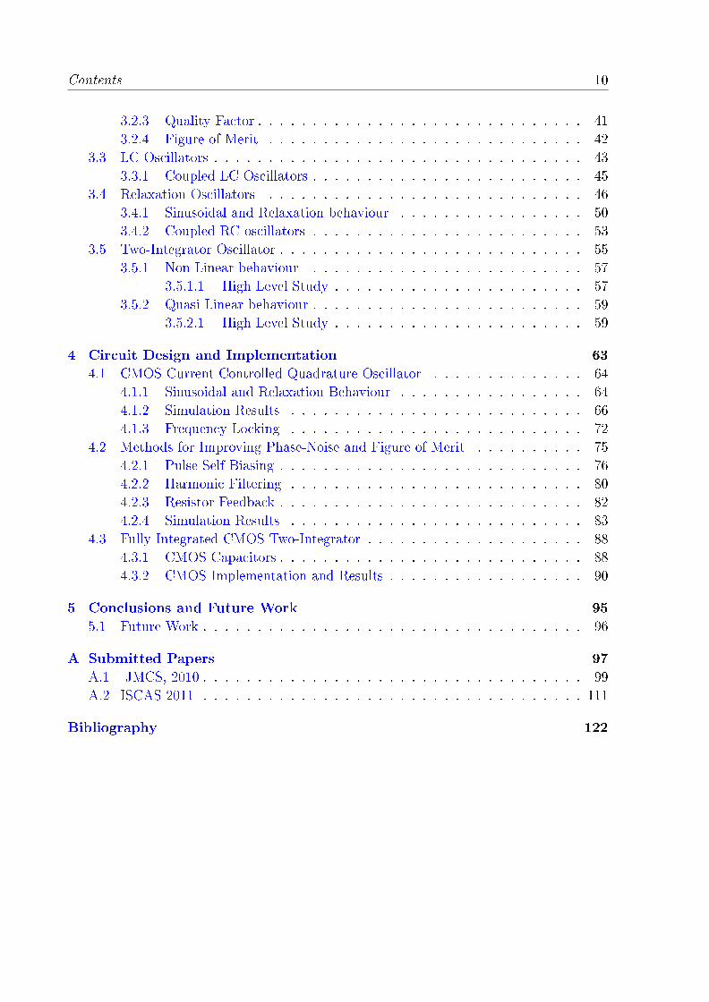
Contents 10
3.2.3 Quality Factor . . . . . . . . . . . . . . . . . . . . . . . . . . . . . . 41
3.2.4 Figure of Merit . . . . . . . . . . . . . . . . . . . . . . . . . . . . . 42
3.3 LC Oscillators . . . . . . . . . . . . . . . . . . . . . . . . . . . . . . . . . . 43
3.3.1 Coupled LC Oscillators . . . . . . . . . . . . . . . . . . . . . . . . . 45
3.4 Relaxation Oscillators . . . . . . . . . . . . . . . . . . . . . . . . . . . . . 46
3.4.1 Sinusoidal and Relaxation behaviour . . . . . . . . . . . . . . . . . 50
3.4.2 Coupled RC oscillators . . . . . . . . . . . . . . . . . . . . . . . . . 53
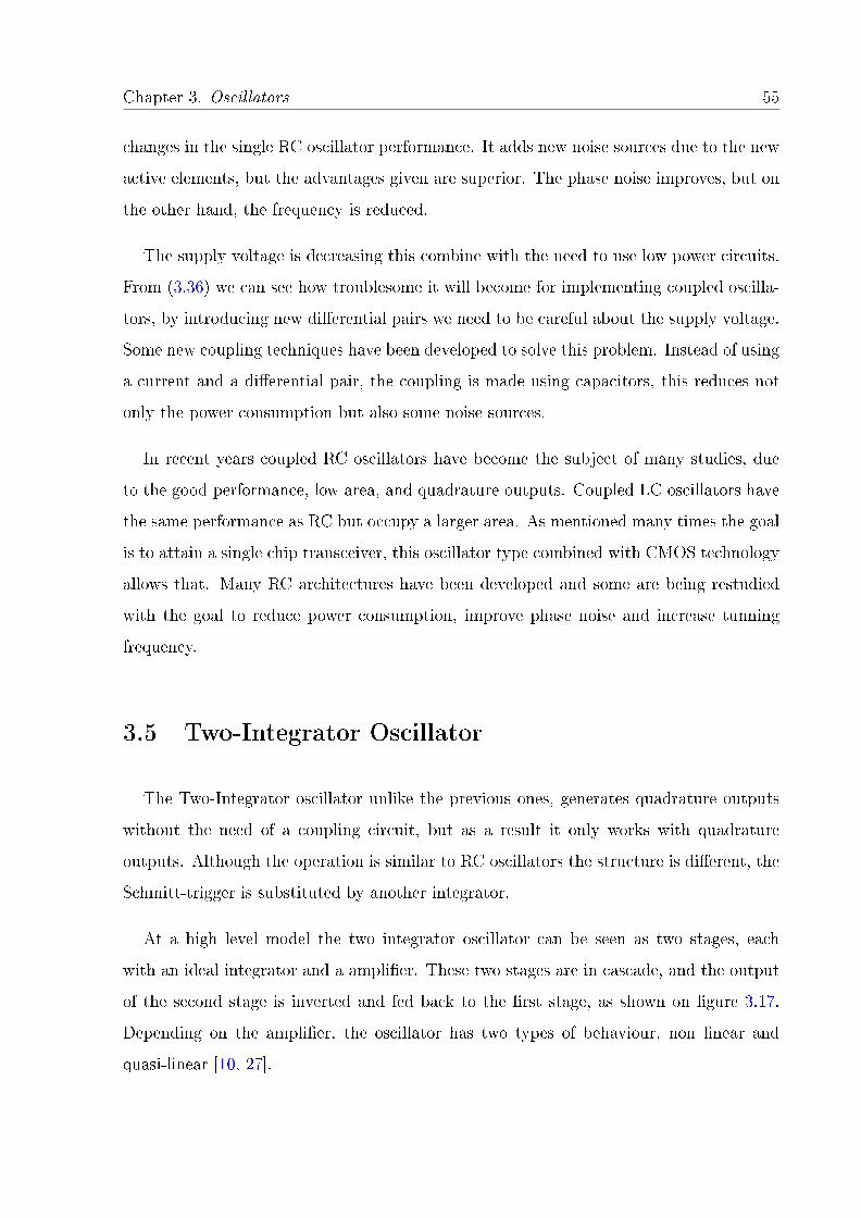
3.5 Two-Integrator Oscillator . . . . . . . . . . . . . . . . . . . . . . . . . . . . 55
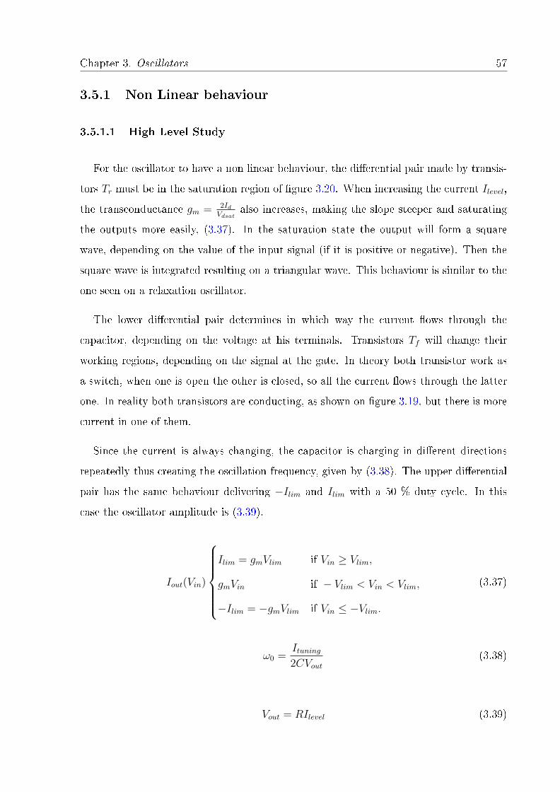
3.5.1 Non Linear behaviour . . . . . . . . . . . . . . . . . . . . . . . . . 57
3.5.1.1 High Level Study . . . . . . . . . . . . . . . . . . . . . . . 57
3.5.2 Quasi Linear behaviour . . . . . . . . . . . . . . . . . . . . . . . . . 59
3.5.2.1 High Level Study . . . . . . . . . . . . . . . . . . . . . . . 59
4 Circuit Design and Implementation 63
4.1 CMOS Current Controlled Quadrature Oscillator . . . . . . . . . . . . . . 64
4.1.1 Sinusoidal and Relaxation Behaviour . . . . . . . . . . . . . . . . . 64
4.1.2 Simulation Results . . . . . . . . . . . . . . . . . . . . . . . . . . . 66
4.1.3 Frequency Locking . . . . . . . . . . . . . . . . . . . . . . . . . . . 72
4.2 Methods for Improving Phase-Noise and Figure of Merit . . . . . . . . . . 75
4.2.1 Pulse Self Biasing . . . . . . . . . . . . . . . . . . . . . . . . . . . . 76
4.2.2 Harmonic Filtering . . . . . . . . . . . . . . . . . . . . . . . . . . . 80
4.2.3 Resistor Feedback . . . . . . . . . . . . . . . . . . . . . . . . . . . . 82
4.2.4 Simulation Results . . . . . . . . . . . . . . . . . . . . . . . . . . . 83
4.3 Fully Integrated CMOS Two-Integrator . . . . . . . . . . . . . . . . . . . . 88
4.3.1 CMOS Capacitors . . . . . . . . . . . . . . . . . . . . . . . . . . . . 88
4.3.2 CMOS Implementation and Results . . . . . . . . . . . . . . . . . . 90
5 Conclusions and Future Work 95
5.1 Future Work . . . . . . . . . . . . . . . . . . . . . . . . . . . . . . . . . . . 96
A Submitted Papers 97
A.1 JMCS, 2010 . . . . . . . . . . . . . . . . . . . . . . . . . . . . . . . . . . . 99
A.2 ISCAS 2011 . . . . . . . . . . . . . . . . . . . . . . . . . . . . . . . . . . . 111
Bibliography 122
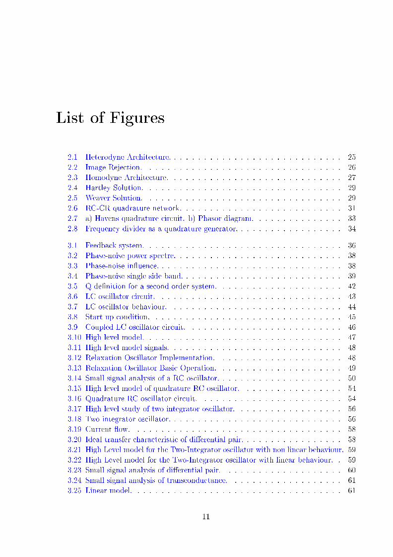
List of Figures
2.1 Heterodyne Architecture. . . . . . . . . . . . . . . . . . . . . . . . . . . . . 25
2.2 Image Rejection. . . . . . . . . . . . . . . . . . . . . . . . . . . . . . . . . 26
2.3 Homodyne Architecture. . . . . . . . . . . . . . . . . . . . . . . . . . . . . 27
2.4 Hartley Solution. . . . . . . . . . . . . . . . . . . . . . . . . . . . . . . . . 29
2.5 Weaver Solution. . . . . . . . . . . . . . . . . . . . . . . . . . . . . . . . . 29
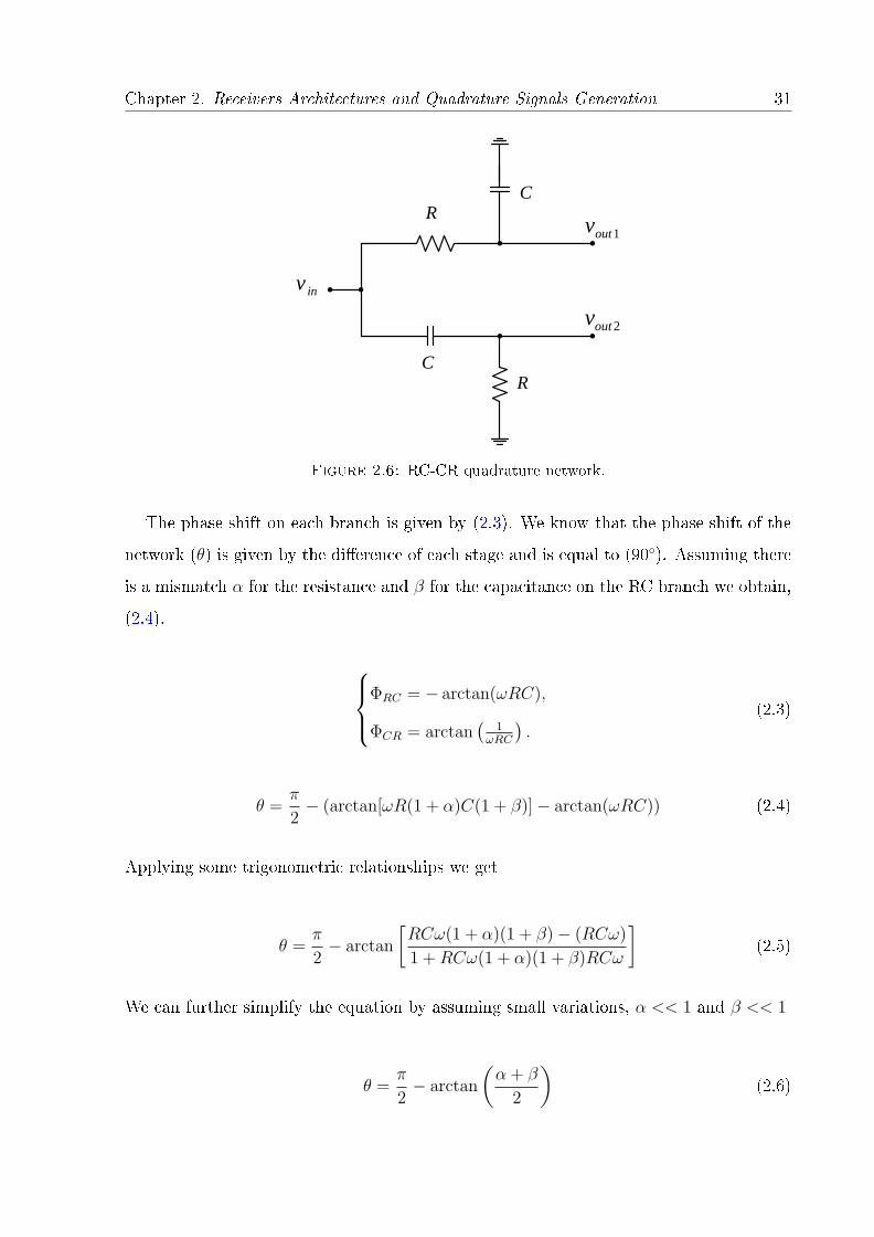
2.6 RC-CR quadrature network. . . . . . . . . . . . . . . . . . . . . . . . . . . 31
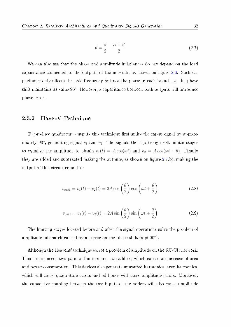
2.7 a) Havens quadrature circuit. b) Phasor diagram. . . . . . . . . . . . . . . 33
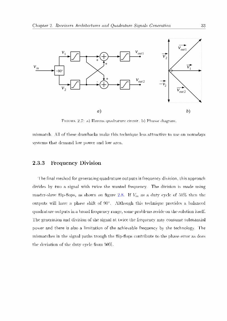
2.8 Frequency divider as a quadrature generator. . . . . . . . . . . . . . . . . . 34
3.1 Feedback system. . . . . . . . . . . . . . . . . . . . . . . . . . . . . . . . . 36
3.2 Phase-noise power spectre. . . . . . . . . . . . . . . . . . . . . . . . . . . . 38
3.3 Phase-noise inuence. . . . . . . . . . . . . . . . . . . . . . . . . . . . . . . 38
3.4 Phase-noise single side band. . . . . . . . . . . . . . . . . . . . . . . . . . . 39
3.5 Q denition for a second order system. . . . . . . . . . . . . . . . . . . . . 42
3.6 LC oscillator circuit. . . . . . . . . . . . . . . . . . . . . . . . . . . . . . . 43
3.7 LC oscillator behaviour. . . . . . . . . . . . . . . . . . . . . . . . . . . . . 44
3.8 Start up condition. . . . . . . . . . . . . . . . . . . . . . . . . . . . . . . . 45
3.9 Coupled LC oscillator circuit. . . . . . . . . . . . . . . . . . . . . . . . . . 46
3.10 High level model. . . . . . . . . . . . . . . . . . . . . . . . . . . . . . . . . 47
3.11 High level model signals. . . . . . . . . . . . . . . . . . . . . . . . . . . . . 48
3.12 Relaxation Oscillator Implementation. . . . . . . . . . . . . . . . . . . . . 48
3.13 Relaxation Oscillator Basic Operation. . . . . . . . . . . . . . . . . . . . . 49
3.14 Small signal analysis of a RC oscillator. . . . . . . . . . . . . . . . . . . . . 50
3.15 High level model of quadrature RC oscillator. . . . . . . . . . . . . . . . . 54
3.16 Quadrature RC oscillator circuit. . . . . . . . . . . . . . . . . . . . . . . . 54
3.17 High level study of two integrator oscillator. . . . . . . . . . . . . . . . . . 56
3.18 Two integrator oscillator. . . . . . . . . . . . . . . . . . . . . . . . . . . . . 56
3.19 Current ow. . . . . . . . . . . . . . . . . . . . . . . . . . . . . . . . . . . 58
3.20 Ideal transfer characteristic of dierential pair. . . . . . . . . . . . . . . . . 58
3.21 High Level model for the Two-Integrator oscillator with non linear behaviour. 59
3.22 High Level model for the Two-Integrator oscillator with linear behaviour. . 59
3.23 Small signal analysis of dierential pair. . . . . . . . . . . . . . . . . . . . 60
3.24 Small signal analysis of transconductance. . . . . . . . . . . . . . . . . . . 61
3.25 Linear model. . . . . . . . . . . . . . . . . . . . . . . . . . . . . . . . . . . 61
11
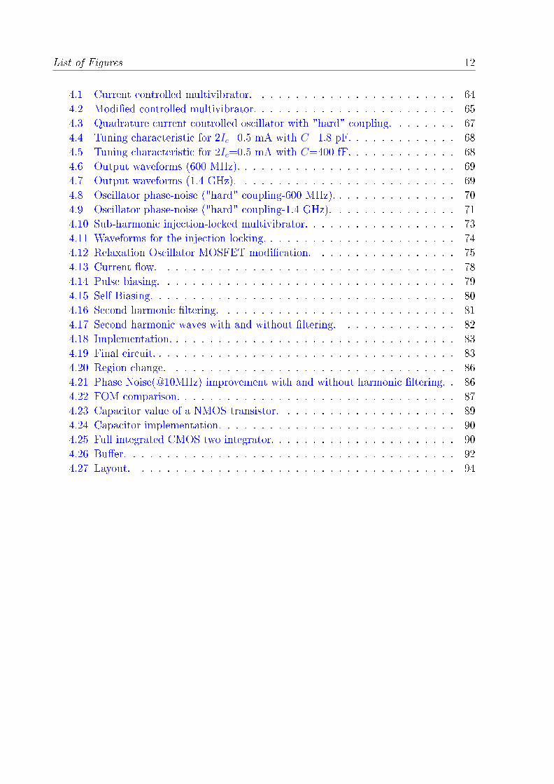
List of Figures 12
4.1 Current controlled multivibrator. . . . . . . . . . . . . . . . . . . . . . . . 64
4.2 Modied controlled multivibrator. . . . . . . . . . . . . . . . . . . . . . . . 65
4.3 Quadrature current controlled oscillator with "hard" coupling. . . . . . . . 67
4.4 Tuning characteristic for 2Ic=0.5 mA with C=1.8 pF. . . . . . . . . . . . . 68
4.5 Tuning characteristic for 2Ic=0.5 mA with C=400 fF. . . . . . . . . . . . . 68
4.6 Output waveforms (600 MHz). . . . . . . . . . . . . . . . . . . . . . . . . . 69
4.7 Output waveforms (1.4 GHz). . . . . . . . . . . . . . . . . . . . . . . . . . 69
4.8 Oscillator phase-noise ("hard" coupling-600 MHz). . . . . . . . . . . . . . . 70
4.9 Oscillator phase-noise ("hard" coupling-1.4 GHz). . . . . . . . . . . . . . . 71
4.10 Sub-harmonic injection-locked multivibrator. . . . . . . . . . . . . . . . . . 73
4.11 Waveforms for the injection locking. . . . . . . . . . . . . . . . . . . . . . . 74
4.12 Relaxation Oscillator MOSFET modication. . . . . . . . . . . . . . . . . 75
4.13 Current ow. . . . . . . . . . . . . . . . . . . . . . . . . . . . . . . . . . . 78
4.14 Pulse biasing. . . . . . . . . . . . . . . . . . . . . . . . . . . . . . . . . . . 79
4.15 Self Biasing. . . . . . . . . . . . . . . . . . . . . . . . . . . . . . . . . . . . 80
4.16 Second harmonic ltering. . . . . . . . . . . . . . . . . . . . . . . . . . . . 81
4.17 Second harmonic waves with and without ltering. . . . . . . . . . . . . . 82
4.18 Implementation. . . . . . . . . . . . . . . . . . . . . . . . . . . . . . . . . . 83
4.19 Final circuit. . . . . . . . . . . . . . . . . . . . . . . . . . . . . . . . . . . . 83
4.20 Region change. . . . . . . . . . . . . . . . . . . . . . . . . . . . . . . . . . 86
4.21 Phase Noise(@10MHz) improvement with and without harmonic ltering. . 86
4.22 FOM comparison. . . . . . . . . . . . . . . . . . . . . . . . . . . . . . . . . 87
4.23 Capacitor value of a NMOS transistor. . . . . . . . . . . . . . . . . . . . . 89
4.24 Capacitor implementation. . . . . . . . . . . . . . . . . . . . . . . . . . . . 90
4.25 Full integrated CMOS two integrator. . . . . . . . . . . . . . . . . . . . . . 90
4.26 Buer. . . . . . . . . . . . . . . . . . . . . . . . . . . . . . . . . . . . . . . 92
4.27 Layout. . . . . . . . . . . . . . . . . . . . . . . . . . . . . . . . . . . . . . 94
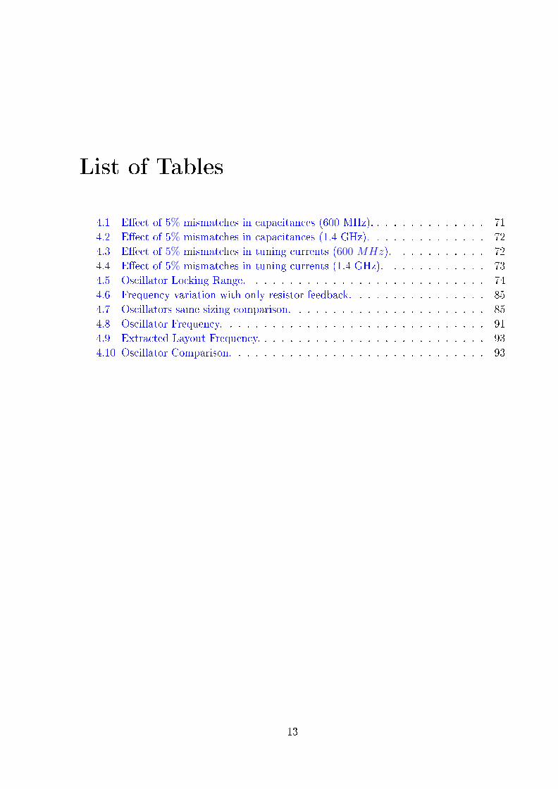
List of Tables
4.1 Eect of 5% mismatches in capacitances (600 MHz). . . . . . . . . . . . . . 71
4.2 Eect of 5% mismatches in capacitances (1.4 GHz). . . . . . . . . . . . . . 72
4.3 Eect of 5% mismatches in tuning currents (600 MHz). . . . . . . . . . . 72
4.4 Eect of 5% mismatches in tuning currents (1.4 GHz). . . . . . . . . . . . 73
4.5 Oscillator Locking Range. . . . . . . . . . . . . . . . . . . . . . . . . . . . 74
4.6 Frequency variation with only resistor feedback. . . . . . . . . . . . . . . . 85
4.7 Oscillators same sizing comparison. . . . . . . . . . . . . . . . . . . . . . . 85
4.8 Oscillator Frequency. . . . . . . . . . . . . . . . . . . . . . . . . . . . . . . 91
4.9 Extracted Layout Frequency. . . . . . . . . . . . . . . . . . . . . . . . . . . 93
4.10 Oscillator Comparison. . . . . . . . . . . . . . . . . . . . . . . . . . . . . . 93
13

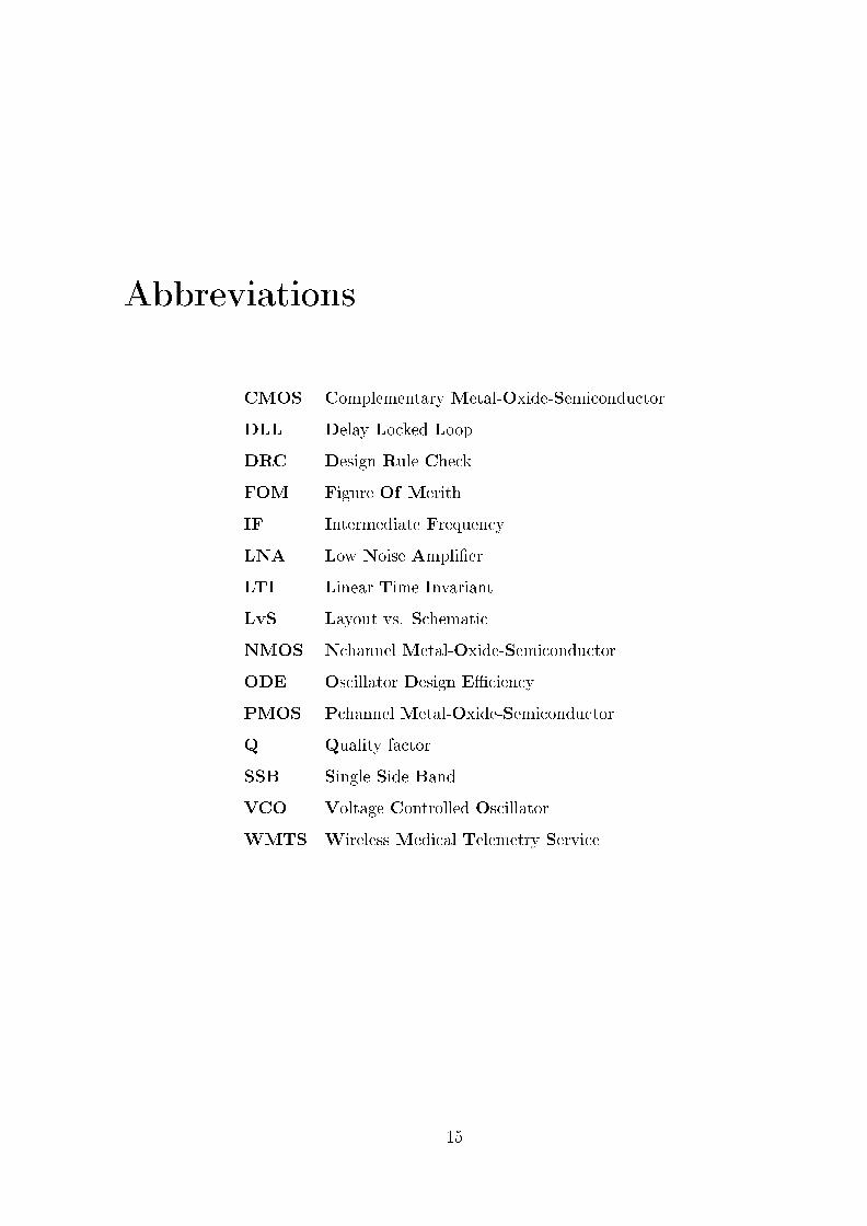
Abbreviations
CMOS Complementary Metal-Oxide-Semiconductor
DLL Delay Locked Loop
DRC Design Rule Check
FOM Figure Of Merith
IF Intermediate Frequency
LNA Low Noise Amplier
LTI Linear Time Invariant
LvS Layout vs. Schematic
NMOS Nchannel Metal-Oxide-Semiconductor
ODE Oscillator Design Eciency
PMOS Pchannel Metal-Oxide-Semiconductor
Q Quality factor
SSB Single Side Band
VCO Voltage Controlled Oscillator
WMTS Wireless Medical Telemetry Service
15


Dedicated to my Family. . .
17

Chapter 1
Introduction
1.1 Background
Wireless communication evolution through out the years have been inuenced by many
factors like power consumption, size, cost, and noise. Nowadays, the boom on wireless
communications led to new requirements such as: low supply voltage, low cost, and small
area circuits. The use of CMOS technologies is a way to attain these objectives, by
adapting old architectures or by implementing new circuit designs.
The RF front-end is generally dened as the circuits between the antenna and the
digital part. The receiver front-end has the most crucial role in communications, their
blocks have very demanding specications. There are two basic architectures: heterodyne
and homodyne, the rst converts the signal to a intermediate frequency (IF) and the
latter downconverts directly to the baseband. The Low-IF receiver is a modied version
of the homodyne and is becoming a good alternative, because it combines the advantages
of both basic architectures.
Modern receivers demand quadrature outputs, so the oscillator must be able to gener-
ate wave signals with a 90 phase shift, so the outputs must be stable in frequency and
phase otherwise any deviation may compromise the system. One way to obtain accu-
rate quadratures outputs is cross coupling two symmetric oscillators. Due to this, new
19
Chapter 1. Introduction 20
architectures have emerged using RC and LC oscillators, some of them have inherent
quadrature outputs, for example the two integrator oscillator.
When comparing a single LC and RC oscillator, the rst one has a better phase-noise.
To reduce the discrepancy new techniques have been develop for this purpose. With new
market requirements and the study of cross coupled oscillators the RC oscillators have
proved to be a good choice for quadrature outputs, coupled LC oscillators on the contrary
have a higher phase-noise, due to the degradation of the quality factor (Q), [10]. There are
other advantages such as fast synchronization, wide frequency tuning range, and low area.
Recent studies of RC oscillators in CMOS technology, have demonstrated the possibility
to integrate other receiver blocks within the oscillator circuit, [10]. The main objective of
this thesis is to show the advantages mentioned through three dierent RC circuits.
1.2 Motivation
The main motivation is the study of quadrature oscillators with reduced area, power,
and low phase noise, for modern low-IF and direct conversion receivers. In this thesis we
present three dierent approaches to this matter. In the rst part we will simulate the
behaviour of a coupled RC oscillator when some of his components are mismatched, we
will also see how much time a single and coupled oscillator takes to synchronize when
an external current source with a frequency equal to an odd multiple of the oscillation
frequency. Then we will apply some methods to a simple RC oscillator with the objective
of improving power consumption and noise. These segments serve to prove the advan-
tages of RC oscillators and how some of their disadvantages can be surpassed. We have
implemented a fully integrated CMOS two integrator to reinforce the idea of a small area
circuit, the total area occupied is 5.856x10⁻³ mm2.

Chapter 1. Introduction 21
1.3 Thesis Organization
This thesis is organized in ve chapters. The current one gives an introduction to the
work done, the motivation, the structure of this thesis, and the main contributions.
The second chapter focus on receiver architectures, their dierences and features. We
will also discuss conventional quadrature signal generators.
In chapter three we present some oscillator basics and analyse three dierent oscillators
architectures. The rst is a LC oscillator known for its low noise, the second is RC
oscillators that have been the focus of many studies in recent years, the last is the two
integrator oscillator, a oscillator that has quadrature outputs. We also discuss how RC
and LC oscillators can produce quadrature outputs.
The main chapter of this thesis is the fourth one. Here we discuss, analyse and im-
plement dierent oscillators. These circuits are designed with the objective of obtaining
reduced noise, power and area circuits. First, we tested a RC oscillator for component
mismatches and how they aect the behaviour of the oscillator. In the second part we
implement some methods to reduce phase noise, and nally, we present a fully integrated
CMOS two integrator with the respective layout and post-layout simulations. All oscilla-
tors were implemented in Cadence software using 0.13 µm CMOS technology.
In the fth chapter we present some conclusions and indicate some future research work
that can be done concerning the topics of this thesis.
Chapter 1. Introduction 22
1.4 Main Contributions
The main contributions for this thesis are:
− The study and simulation of numerous techniques to reduce phase noise applied on
a simple relaxation oscillator is made. One of them is unique and only possible
on CMOS. A paper was submitted, at the moment of writing this thesis we were
waiting for approval.
− The study of a multivibrator for CMOS technology. The utilization of that oscil-
lator for a cross coupled version using both soft and rigid coupling, and comparing
both. The study of frequency locking at a sub-harmonic frequency when an external
current source is applied. This work lead to a article [1] for the MIXDES conference,
where it received one of the awards for outstanding paper, and it was invited for an
extended version for a magazine.
− The creation of a fully integrated CMOS two integrator oscillator, by substituting
the capacitors and resistors for CMOS transistors, making it a low cost, low power
and small area oscillator. A layout was made for a future test-chip, at the present
this chip was submitted for fabrication. If the chip results are satisfactory, then this
work may have a future publication.
Chapter 2
Receivers Architectures and
Quadrature Signals Generation
2.1 Introduction
In this chapter we present a brief introduction to some receiver architectures and the
last part will focus on some conventional quadrature signal generators.
Receivers are used for demodulation of a signal sent by a transmitter, rst the received
signal in the antenna is amplied and then downconverted to a lower frequency at the
end we obtain the demodulated signal at the output. The transmitter performs the op-
posite actions, it modulates the signal, then upconverts and nally amplies and sends it
through the antenna. Both transmitter and receivers can be classied as in two basic ar-
chitectures: homodyne or heterodyne [10, 13]. In heterodyne the signal is downconverted
to intermediate frequencies (IF), in the homodyne the conversion is done directly to the
baseband. Nowadays the homodyne architecture is preferred because of its simplicity,
lower power and low cost [10]. New architectures have appeared in recent years based on
the ones mentioned, one of them is being used on FM receivers it is called low IF receiver
[13].
23
Chapter 2. Receivers Architectures and Quadrature Signals Generation 24
The signal received in the antenna goes through many stages in the receiver, each one
with a specic role. The amplier is the rst main block and has a crucial inuence on
the overall noise that why the LNA as to amplify the signal without introducing noise.
Another block is the oscillator, this block generates a frequency, which combined with the
mixer will change the signal frequency.
Modern receivers require quadrature outputs, due to this the oscillator must be able to
generate two waveforms with a 90 dierence between them. The last part of this chap-
ter presents some methods to generate quadrature outputs without feedback topologies.
First, we discuss a basic circuit using known electronic components, then more complex
architectures such as Havens' technique and frequency division.
2.2 Receivers
There are three popular architectures of receivers heterodyne, homodyne and low-IF,
[10, 13]. The rst one is widely used, in a rst stage the signal goes from RF to IF
and on a second stage from IF to the baseband. The second receiver translates the signal
directly from the RF to the baseband, that is why they are also called direct IF or Zero-IF
architectures. The low-If receiver is based on the heterodyne, the signal goes from RF to
a low-IF frequency and only after its conversion to the digital domain, is brought to the
baseband.
2.2.1 Heterodyne or IF Receivers
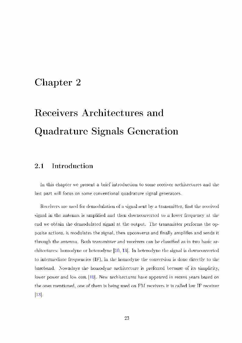
The block diagram of a modern heterodyne is shown gure 2.1. The incoming signal
is rst passed through a band pass lter, which isolates the wanted frequencies, then it
is amplied by the LNA. The image reject lter attenuates the signals at image band
frequencies from the LNA. With the mixer and the oscillator, the signal goes to IF then
another band pass lter is applied to obtain the IF band of interest and reject the others
and nally is amplied. The downconversion requires both in-phase (I) and quadrature
Chapter 2. Receivers Architectures and Quadrature Signals Generation 25
(Q) components of the signal so the mixer can bring it to the baseband. After that, the
signal goes through a low pass lter and then is converted to digital. All lters used must
be implemented o-chip to obtain a high quality factor (Q), this is one of the reasons why
this architecture is not used in nowadays technology. There are two main drawbacks of
this architecture, the need for a high performance oscillator and the image frequency.
A/D
A/D
DSPLO2
-90°LO1
LNA Image
reject
BPF
Channel
select
BPF
Figure 2.1: Heterodyne Architecture.
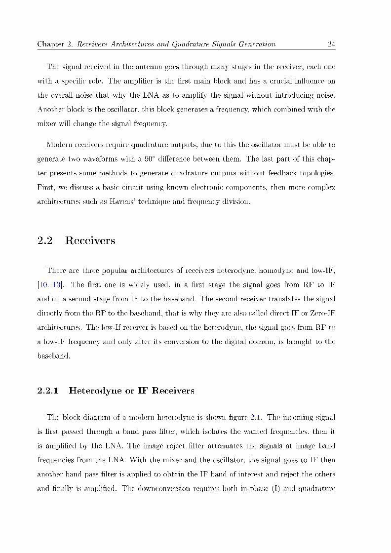
The image frequency problem is caused by the mixer, it moves both sum and dierence
frequencies, converting two frequencies at the same IF. We want to downconvert a signal
with a frequency ωRF to ωIF , but the image frequency at ωIM , as shown on gure 2.2 is
also downconverted. Even after the image reject lter there is still a small signal at that
frequency. When the signal goes through the mixer both frequency are downconverted to
ωIF . Let us give a practical example, assuming that ωIM is 6 GHz, ωLO is 4 GHz and ωRF
is 2 GHz, when both frequencies pass the mixer both end up at 2 GHz.
There is a trade-o in this architecture related to the IF frequency. The value chosen
inuences some blocks of the receiver. With higher value it becomes easier to design an
image rejection lter, because the image is far away from the desired frequency. At a
lower value the band pass lter next to the mixer is less demanding making it easier to
implement, the same goes for the IF signal amplier.
Chapter 2. Receivers Architectures and Quadrature Signals Generation 26
LO1
LNA Image
reject
BPF
Channel
select
BPF
RF LO IM
RF LO IMIF
RF IF
Figure 2.2: Image Rejection.
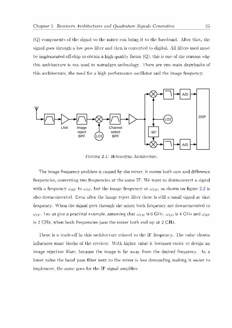
2.2.2 Homodyne or Zero IF Receivers
In homodyne receivers the signal is directly translated from the RF to baseband. The
most obvious dierence between homodyne and heterodyne is the absence of a mixer stage,
which is why the band ltering is only made before the LNA and after the downconvertion.
In the heterodyne, as seen before, the rst mixer causes a overlap between two signals
on IF, in this case since the IF is zero the desired frequency is its own image, so there
is no need for a image reject lter. Other advantage is amplication, since it is done on
baseband the power consumption is reduced. Furthermore there is no need to use a band
pass lter, instead, only a low pass lter is used after the downconversion. Since there is
no image reject lter the LNA does not need to match 50 ohm. This architecture as less
blocks, as shown on gure 2.3, thus, consuming less power than the heterodyne receiver.
There are some disadvantages when compared with the heterodyne, but this archi-
tecture is still in research for more demanding applications [10]. Those disadvantages
are:
− Local oscillator leakage, normally, there will be a imperfect isolation between the
local oscillator and the input port of the mixer and LNA, this leakage mixes with
the original wave from the oscillator producing DC osets in the mixer output.
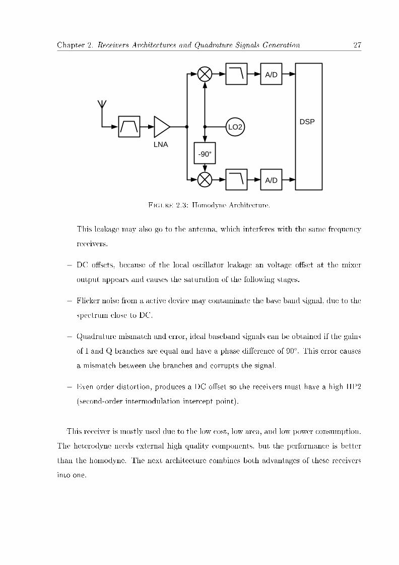
Chapter 2. Receivers Architectures and Quadrature Signals Generation 27
A/D
A/D
DSPLO2
-90°
LNA
Figure 2.3: Homodyne Architecture.
This leakage may also go to the antenna, which interferes with the same frequency
receivers.
− DC osets, because of the local oscillator leakage an voltage oset at the mixer
output appears and causes the saturation of the following stages.
− Flicker noise from a active device may contaminate the base band signal, due to the
spectrum close to DC.
− Quadrature mismatch and error, ideal baseband signals can be obtained if the gains
of I and Q branches are equal and have a phase dierence of 90. This error causes
a mismatch between the branches and corrupts the signal.
− Even order distortion, produces a DC oset so the receivers must have a high IIP2
(second-order intermodulation intercept point).
This receiver is mostly used due to the low cost, low area, and low power consumption.
The heterodyne needs external high quality components, but the performance is better
than the homodyne. The next architecture combines both advantages of these receivers
into one.
Chapter 2. Receivers Architectures and Quadrature Signals Generation 28
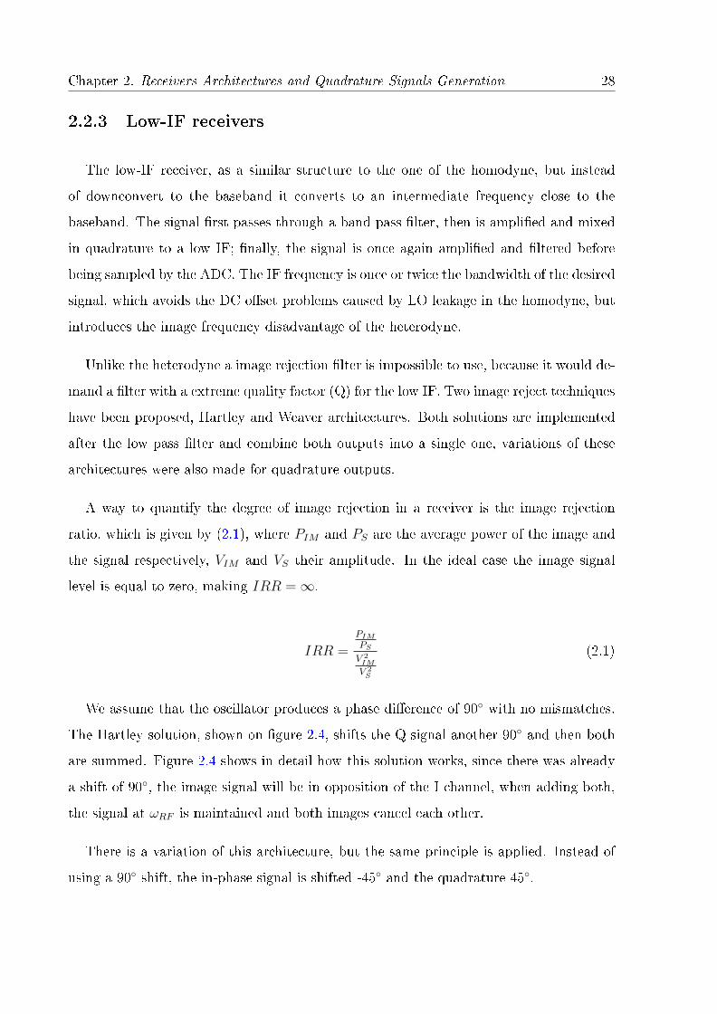
2.2.3 Low-IF receivers
The low-IF receiver, as a similar structure to the one of the homodyne, but instead
of downconvert to the baseband it converts to an intermediate frequency close to the
baseband. The signal rst passes through a band pass lter, then is amplied and mixed
in quadrature to a low IF; nally, the signal is once again amplied and ltered before
being sampled by the ADC. The IF frequency is once or twice the bandwidth of the desired
signal, which avoids the DC oset problems caused by LO leakage in the homodyne, but
introduces the image frequency disadvantage of the heterodyne.
Unlike the heterodyne a image rejection lter is impossible to use, because it would de-
mand a lter with a extreme quality factor (Q) for the low IF. Two image reject techniques
have been proposed, Hartley and Weaver architectures. Both solutions are implemented
after the low pass lter and combine both outputs into a single one, variations of these
architectures were also made for quadrature outputs.
A way to quantify the degree of image rejection in a receiver is the image rejection
ratio, which is given by (2.1), where PIM and PS are the average power of the image and
the signal respectively, VIM and VS their amplitude. In the ideal case the image signal
level is equal to zero, making IRR =∞.
IRR =
PIM
PS
V 2IM
V 2S
(2.1)
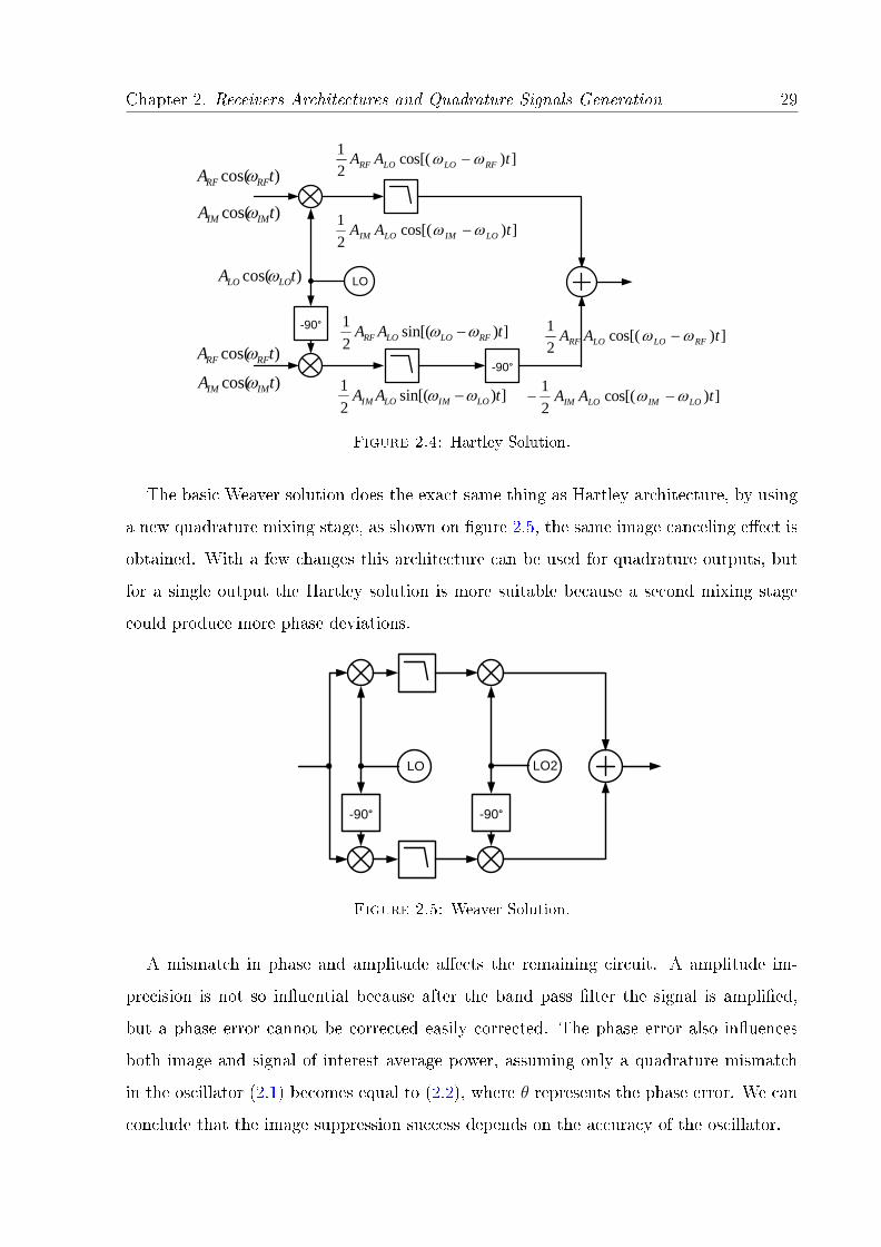
We assume that the oscillator produces a phase dierence of 90 with no mismatches.
The Hartley solution, shown on gure 2.4, shifts the Q signal another 90 and then both
are summed. Figure 2.4 shows in detail how this solution works, since there was already
a shift of 90, the image signal will be in opposition of the I channel, when adding both,
the signal at ωRF is maintained and both images cancel each other.
There is a variation of this architecture, but the same principle is applied. Instead of
using a 90 shift, the in-phase signal is shifted -45 and the quadrature 45.
Chapter 2. Receivers Architectures and Quadrature Signals Generation 29
LO
-90°
)cos( tA LOLO
)cos( tA RFRF
)cos( tA RFRF
)cos( tA IMIM
)cos( tA IMIM
])cos[(2
1tAA RFLOLORF
])cos[(2
1tAA LOIMLOIM
])sin[(2
1tAA RFLOLORF
])sin[(2
1tAA LOIMLOIM
-90°
])cos[(2
1tAA RFLOLORF
])cos[(2
1tAA LOIMLOIM
Figure 2.4: Hartley Solution.
The basic Weaver solution does the exact same thing as Hartley architecture, by using
a new quadrature mixing stage, as shown on gure 2.5, the same image canceling eect is
obtained. With a few changes this architecture can be used for quadrature outputs, but
for a single output the Hartley solution is more suitable because a second mixing stage
could produce more phase deviations.
LO
-90° -90°
LO2
Figure 2.5: Weaver Solution.
A mismatch in phase and amplitude aects the remaining circuit. A amplitude im-
precision is not so inuential because after the band pass lter the signal is amplied,
but a phase error cannot be corrected easily corrected. The phase error also inuences
both image and signal of interest average power, assuming only a quadrature mismatch
in the oscillator (2.1) becomes equal to (2.2), where θ represents the phase error. We can
conclude that the image suppression success depends on the accuracy of the oscillator.
Chapter 2. Receivers Architectures and Quadrature Signals Generation 30
IRR =θ2
4(2.2)
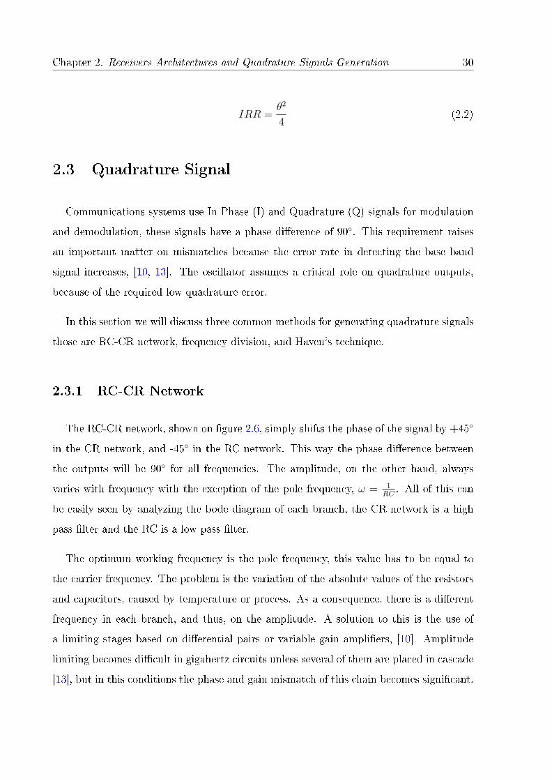
2.3 Quadrature Signal
Communications systems use In-Phase (I) and Quadrature (Q) signals for modulation
and demodulation, these signals have a phase dierence of 90. This requirement raises
an important matter on mismatches because the error rate in detecting the base band
signal increases, [10, 13]. The oscillator assumes a critical role on quadrature outputs,
because of the required low quadrature error.
In this section we will discuss three common methods for generating quadrature signals
those are RC-CR network, frequency division, and Haven's technique.
2.3.1 RC-CR Network
The RC-CR network, shown on gure 2.6, simply shifts the phase of the signal by +45
in the CR network, and -45 in the RC network. This way the phase dierence between
the outputs will be 90 for all frequencies. The amplitude, on the other hand, always
varies with frequency with the exception of the pole frequency, ω = 1RC
. All of this can
be easily seen by analyzing the bode diagram of each branch, the CR network is a high
pass lter and the RC is a low pass lter.
The optimum working frequency is the pole frequency, this value has to be equal to
the carrier frequency. The problem is the variation of the absolute values of the resistors
and capacitors, caused by temperature or process. As a consequence, there is a dierent
frequency in each branch, and thus, on the amplitude. A solution to this is the use of
a limiting stages based on dierential pairs or variable gain ampliers, [10]. Amplitude
limiting becomes dicult in gigahertz circuits unless several of them are placed in cascade
[13], but in this conditions the phase and gain mismatch of this chain becomes signicant.
Chapter 2. Receivers Architectures and Quadrature Signals Generation 31
R
RC
C
inv
1outv
2outv
Figure 2.6: RC-CR quadrature network.
The phase shift on each branch is given by (2.3). We know that the phase shift of the
network (θ) is given by the dierence of each stage and is equal to (90). Assuming there
is a mismatch α for the resistance and β for the capacitance on the RC branch we obtain,
(2.4).
ΦRC = − arctan(ωRC),
ΦCR = arctan(
1ωRC
).
(2.3)
θ =π
2− (arctan[ωR(1 + α)C(1 + β)]− arctan(ωRC)) (2.4)
Applying some trigonometric relationships we get
θ =π
2− arctan
[RCω(1 + α)(1 + β)− (RCω)
1 +RCω(1 + α)(1 + β)RCω
](2.5)
We can further simplify the equation by assuming small variations, α << 1 and β << 1
θ =π
2− arctan
(α + β
2
)(2.6)
Chapter 2. Receivers Architectures and Quadrature Signals Generation 32
θ =π
2− α + β
2(2.7)
We can also see that the phase and amplitude imbalances do not depend on the load
capacitance connected to the outputs of the network, as shown on gure 2.6. Such ca-
pacitance only aects the pole frequency but not the phase in each branch, so the phase
shift maintains its value 90. However, a capacitance between both outputs will introduce
phase error.
2.3.2 Havens' Technique
To produce quadrature outputs this technique rst splits the input signal by approx-
imately 90, generating signal v1 and v2. The signals then go trough soft-limiter stages
to equalize the amplitude to obtain v1(t) = A cos(ωt) and v2 = A cos(ωt + θ). Finally
they are added and subtracted making the outputs, as shown on gure 2.7.b), making the
output of this circuit equal to :
vout1 = v1(t) + v2(t) = 2A cos
(θ
2
)cos
(ωt+
θ
2
)(2.8)
vout1 = v1(t)− v2(t) = 2A sin
(θ
2
)sin
(ωt+
θ
2
)(2.9)
The limiting stages located before and after the signal operations solve the problem of
amplitude mismatch caused by an error on the phase shift (θ 6= 90).
Although the Heavens' technique solves a problem of amplitude on the RC-CR network.
This circuit needs two pairs of limiters and two adders, which causes an increase of area
and power consumption. This devices also generate unwanted harmonics, even harmonics,
which will cause quadrature errors and odd ones will cause amplitude errors. Moreover,
the capacitive coupling between the two inputs of the adders will also cause amplitude
Chapter 2. Receivers Architectures and Quadrature Signals Generation 33
~90°inv
1v
2v
++
+-
1outv
2outv
1v
2v
2v
1outv
2outv
)a )b
Figure 2.7: a) Havens quadrature circuit. b) Phasor diagram.
mismatch. All of these drawbacks make this technique less attractive to use on nowadays
systems that demand low power and low area.
2.3.3 Frequency Division
The nal method for generating quadrature outputs is frequency division, this approach
divides by two a signal with twice the wanted frequency. The division is made using
master-slave ip-ops, as shown on gure 2.8. If Vin as a duty cycle of 50% then the
outputs will have a phase shift of 90. Although this technique provides a balanced
quadrature outputs in a broad frequency range, some problems reside on the solution itself.
The generation and division of the signal at twice the frequency may consume substantial
power and there is also a limitation of the achievable frequency by the technology. The
mismatches in the signal paths trough the ip-ops contribute to the phase error as does
the deviation of the duty cycle from 50%.
Chapter 2. Receivers Architectures and Quadrature Signals Generation 34
Latch
Latch
1outv2outvinv
Figure 2.8: Frequency divider as a quadrature generator.
There are also other techniques that measure the phase imbalance of the quadrature
outputs and correct them, [24]. Some use a delay-locked loop (DLL), where the input
signal is split in two paths, one of them delayed by 90, then a phase detector controls
the current in the phase shifter and adjusts the phase dierent between two split paths.
Another calibration is a rst order phase shifter with a self-calibration loop to tune each
branch of the phase shifter.
In modern communications, voltage controlled oscillator (VCO) architectures with in-
herent quadrature outputs provide a alternative to the techniques mentioned. This can
be accomplished using two cross coupled VCO or a oscillator that has inherent IQ signals,
such as, the two integrator oscillator.
Chapter 3
Oscillators
3.1 Introduction
In the rst part of this chapter, we review the basics for designing a oscillator. Some
important features such as noise and quality factor determine the overall quality and
eciency of a oscillator. It is important to note that, the Barkhausen criterion and the
quality factor denition, can only be applied to oscillators with a linear behaviour. We
will only discuss basic concepts and how they are aected.
This chapter also introduces dierent architectures: LC oscillators, RC oscillators and,
the Two-Integrator. LC oscillators are known for their low phase noise as opposed to the
RC oscillators, but some disadvantages, such as, area and cost make the choice of which
architecture to use more dicult.
As mentioned before quadrature outputs are important in nowadays communications,
but single LC and RC oscillators cannot produce them. We will discuss how two of these
oscillators can generate quadrature outputs, and also, why the two-integrator has inherent
quadrature outputs.
35
Chapter 3. Oscillators 36
3.2 Oscillator Basics
3.2.1 Barkhausen Criteron
A oscillator generates a output signal without an external source. To accomplish that
we need a natural oscillator such as a quartz crystal, or a unstable system where his own
noise creates a periodic signal.
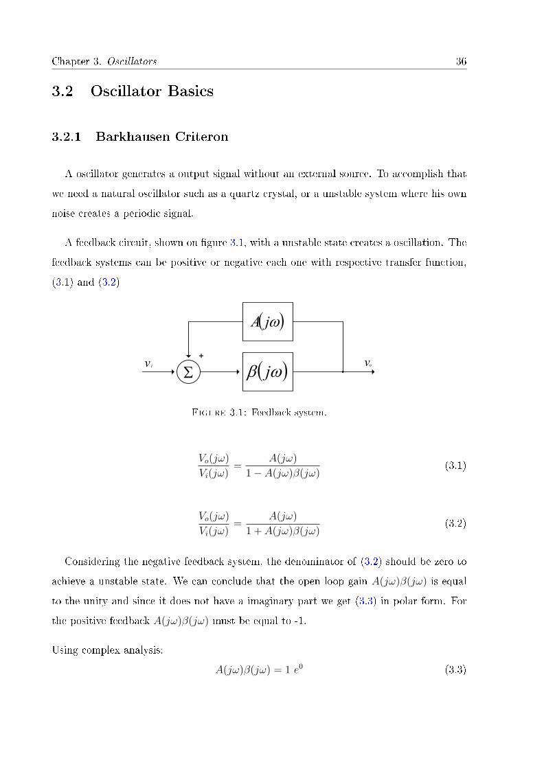
A feedback circuit, shown on gure 3.1, with a unstable state creates a oscillation. The
feedback systems can be positive or negative each one with respective transfer function,
(3.1) and (3.2)
+
Viv i vo
jA
j
Figure 3.1: Feedback system.
Vo(jω)
Vi(jω)=
A(jω)
1− A(jω)β(jω)(3.1)
Vo(jω)
Vi(jω)=
A(jω)
1 + A(jω)β(jω)(3.2)
Considering the negative feedback system, the denominator of (3.2) should be zero to
achieve a unstable state. We can conclude that the open loop gain A(jω)β(jω) is equal
to the unity and since it does not have a imaginary part we get (3.3) in polar form. For
the positive feedback A(jω)β(jω) must be equal to -1.
Using complex analysis:
A(jω)β(jω) = 1 e0 (3.3)
Chapter 3. Oscillators 37
These are the basis for the Barkhausen criterion conditions, which guarantee a stable
oscillation:
|A(jω)β(jω)| = 1 (3.4)
Considering positive feedback
∠A(jω)β(jω) = 0 + 2kπ, k = 0..n, n ∈ N (3.5)
and negative feedback
∠A(jω)β(jω) = π (3.6)
These conditions are not enough for the system to start oscillating. For the oscillator
start-up, the open loop gain initially must be larger than the unity, (3.7).
|A(jω)β(jω)| > 1 (3.7)
After the start-up the feedback and the internal noise will allow the oscillator to reach
a stable state, when the open loop gain complies the rst Barkhausen condition.
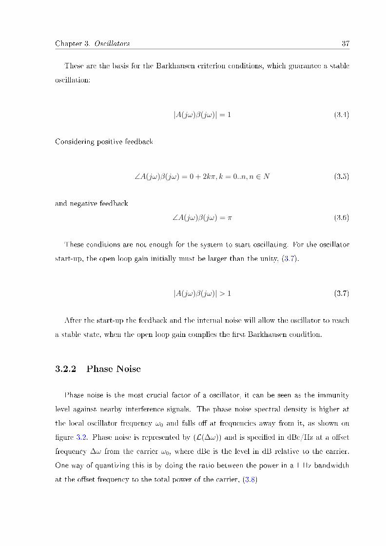
3.2.2 Phase Noise
Phase noise is the most crucial factor of a oscillator, it can be seen as the immunity
level against nearby interference signals. The phase noise spectral density is higher at
the local oscillator frequency ω0 and falls o at frequencies away from it, as shown on
gure 3.2. Phase noise is represented by (L(∆ω)) and is specied in dBc/Hz at a oset
frequency ∆ω from the carrier ω0, where dBc is the level in dB relative to the carrier.
One way of quantizing this is by doing the ratio between the power in a 1 Hz bandwidth
at the oset frequency to the total power of the carrier, (3.8)
Chapter 3. Oscillators 38
Figure 3.2: Phase-noise power spectre.
L(∆ω) =P (∆ω)
P (ω0)(3.8)
Phase noise in the time domain is called jitter noise. We can see how this noise acts
by comparing a noisy sinewave with a relative time grid set by a noiseless sinewave. At
the zero crossing baseline we can see the deviations from the rising edges caused by the
noise. This serves as basis to a time variant approximation of the phase-noise that will
be mentioned, we will also discuss the time invariant approximation of Leeson.
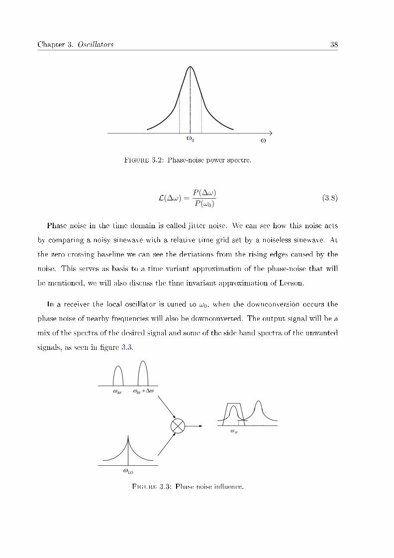
In a receiver the local oscillator is tuned to ω0, when the downconversion occurs the
phase noise of nearby frequencies will also be downconverted. The output signal will be a
mix of the spectra of the desired signal and some of the side band spectra of the unwanted
signals, as seen in gure 3.3.
RF RF
LO
IF
Figure 3.3: Phase-noise inuence.
Chapter 3. Oscillators 39
Passive and active elements of other blocks of the receiver introduce noise, also voltage
and current noise sources through the system inuence noise. All this factors make phase
noise very dicult to predict. However, the noise sources within the oscillator loop have
more inuence on phase noise, [25]. They may be enhanced by the sharp frequency
selectivity of the loop, and become the dominant source of phase noise. The noise on the
loop may also modulate the oscillation frequency.
In an oscillator, phase noise is best described in the frequency domain, where the
spectral density is characterized by measuring the noise sidebands on either side of the
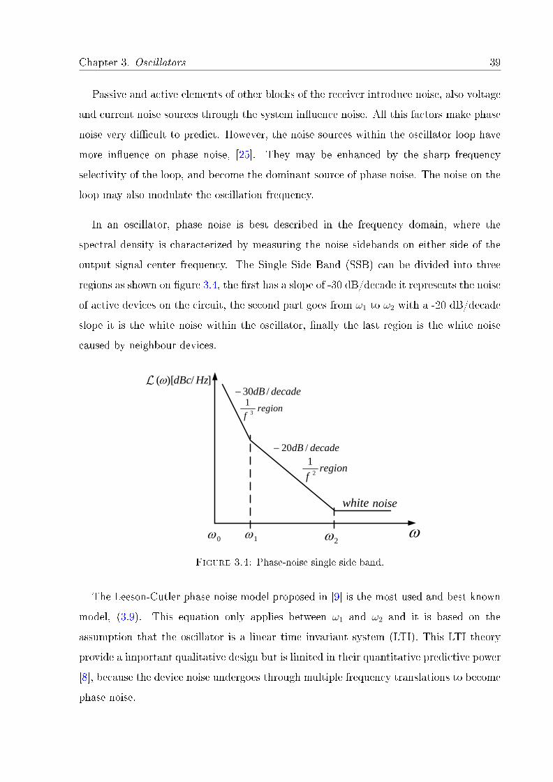
output signal center frequency. The Single Side Band (SSB) can be divided into three
regions as shown on gure 3.4, the rst has a slope of -30 dB/decade it represents the noise
of active devices on the circuit, the second part goes from ω1 to ω2 with a -20 dB/decade
slope it is the white noise within the oscillator, nally the last region is the white noise
caused by neighbour devices.
decadedB /30
decadedB /20
regionf 3
1
regionf 2
1
white noise
0 12
]/)[( HzdBc
Figure 3.4: Phase-noise single side band.
The Leeson-Cutler phase noise model proposed in [9] is the most used and best known
model, (3.9). This equation only applies between ω1 and ω2 and it is based on the
assumption that the oscillator is a linear time invariant system (LTI). This LTI theory
provide a important qualitative design but is limited in their quantitative predictive power
[8], because the device noise undergoes through multiple frequency translations to become
phase noise.
Chapter 3. Oscillators 40
L(∆ω) = 10 log
FkT
2Ps
[1 +
(ω0
2Q∆ω
)2](
1 +∆ω1/f3
|∆ω|
)(3.9)
Where:
k - Boltzman constant;
T - Absolute temperature;
PS - Average power dissipated in the resistive part of the tank;
ω0 - Oscillation frequency;
Q - Quality factor;
∆ω - Oset from the carrier;
∆ω1/f3 - Corner frequency between 1/f 3 and 1/f 2 zones of the noise spectrum;
F - Empirical parameter called excess noise factor.
When comparing the equation to the spectre of the phase noise, shown on gure 3.4
one can conclude that the white noise and the icker noise are represented by (3.10). The
-20 dB/decade region starts at a frequency equal to half bandwidth of the oscillator, in
gure gure 3.4 corresponds to the ω2 frequency.
S(∆ω) =FkT
2Ps
1
∆ω2(3.10)
There have been considerations using oscillators as linear time-varying systems on
[8, 16], where the following equations were reached, (3.11).
L(∆ω) =
10 log
C20
q2max
i2n8∆f∆ω2
ω1/f
∆ω
for 1
f3 region
10 log
10 log[T 2
rms
q2max
i2n4∆f∆ω2
]for 1
f2 region
(3.11)
Where:
Chapter 3. Oscillators 41
i2n/∆f - Noise power spectral density;
∆f - Noise bandwidth;
Γ2rms = 1/π
∫ 2π
0|Γ(x)|2dx =
∑∞n=0C
2n - Root mean square value of Γ(x);
Γ(x) = C0/2 +∑∞
n=1 Cncos(nx+ θn - Impulse sensitivity function;
Cn - Fourier series coecient;
C0 - 0th order of the impulse sensitivity function (fourier series);
θn - phase of the nth harmonic;
ω1/f - Flicker corner frequency of the device;
qmax - Maximum charge stored across the capacitor in the resonator.
3.2.3 Quality Factor
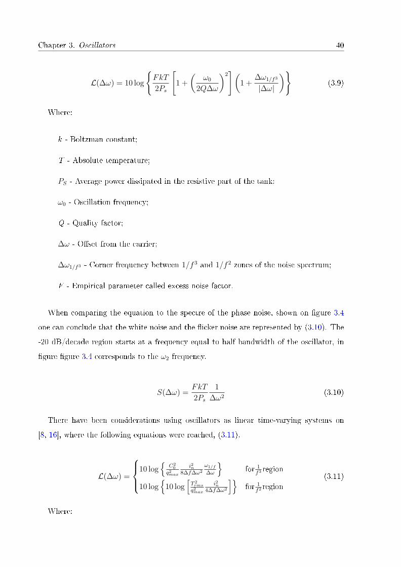
Quality factor is a important feature for a oscillator and is related to the phase noise.
The most general formula used is (3.12). This equation is normally applied to a RLC
resonator. The maximum energy stores is related to the L and C components and the
energy dissipated is associated with the resistor.
Q = 2πMaximum energy stored in a period
Energy dissipated in a period(3.12)
Leeson denes the Q factor, (3.13), considering a resonant circuit with a -3 dB band-
width B and a frequency ω0. In the Leeson-Cutler phase noise model, half bandwidth of
the oscillator is taken into account ω0/2Q. With a high Q factor the bandwidth will be
reduced, as seen in gure 3.5, and the inuence of the 1/f 2 noise on the phase noise will
decrease making the slope starting to disappear, [9, 16]. When this happens the slopes
1/f 3 and 1/f 2 will come close to the carrier frequency and reduces the phase noise.
Q =ω0
B(3.13)
Chapter 3. Oscillators 42
B
0
dB3|)(| sH
Figure 3.5: Q denition for a second order system.
3.2.4 Figure of Merit
Figure of Merit is a characteristic that gives a overall perspective of the oscillator
performance, it is usually used in literature for benchmark comparison. It takes into
account not only the phase noise but also power consumption and frequency, (3.14), Pref
is the reference power level equal to 1 mW and PDC the power consumption in mW. The
inclusion of all three aspects help the designer to achieve an optimal and balanced design,
[26, 27].
FOM = Lmeasured + 10 log
((∆ω
ω0
)2PDCPref
)(3.14)
There is also a gure of merit concerning the layout area, (3.15), where Aref is equal
to 1 mm2 and Achip the circuit area in mm2, [11, 27].
FOMA = Lmeasured + 10 log
((∆ω
ω0
)2PDCPref
AchipAref
)(3.15)
The FOM of an oscillator provides a qualitative insight on the relations between design
parameters, allowing a designer to further optimize the circuit.
There are other FOM that allow a more in depth analysis on the performance of the
oscillator, called Oscillator Design Eciency (ODE), [26, 27]. This benchmark compares
Chapter 3. Oscillators 43
the measure phase noise with a rst order estimation of the best phase noise case achiev-
able, (3.16). This equation is used for LC oscillators, but it as been modied specically
for N-stage ring oscillators [27], such as the Two Integrator (3.17).
ODELC = Lmeasured − 10 log
((kT
2PDC
1
Q2
∆ω
ω0
)2)
(3.16)
ODEring = Lmeasured − 10 log
((N2kT
4PDC
1
(π2)2
∆ω
ω0
)2)
(3.17)
3.3 LC Oscillators
LC oscillators are known for having a quasi linear behaviour and low phase noise, but
because of its elements the circuit area is larger when compared with RC oscillators.
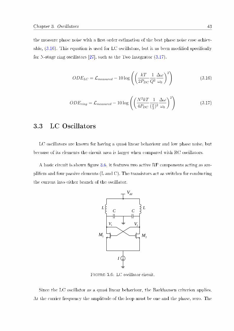
A basic circuit is shown gure 3.6, it features two active RF components acting as am-
pliers and four passive elements (L and C). The transistors act as switches for conducting
the current into either branch of the oscillator.
I
C
2M1M
1V2V
ddV
CL L
Figure 3.6: LC oscillator circuit.
Since the LC oscillator as a quasi linear behaviour, the Barkhausen criterion applies.
At the carrier frequency the amplitude of the loop must be one and the phase, zero. The
Chapter 3. Oscillators 44
last condition is complied because the capacitors give a -90 and the inductors a 90,
giving a total of 0. To understand how the rst condition is attained we can use the
behaviour model of this oscillator presented in gure 3.7.
mg
R L C
Figure 3.7: LC oscillator behaviour.
The open loop gain can be extracted using the impedances of the circuits, the transfer
function A(jω) comes from the transconductance gm of the transistors. The feedback
transfer function (3.18) is formed by the RLC impedance, where R represent losses. At
ω0 the B(jω0) equation only as the real part so the open loop gain |A(jω0)B(jω0)| is equal
to gmR and by the rst Barkhausen condition, gmR = 1. Since the gm cancels R we can
calculate the frequency of this oscillator considering only a LC resonator, (3.20). The Q
factor is given by (3.19)
B(jω) =R
1 + j(ωω0− ω0
ω
)Q
(3.18)
Q = R
√C
L(3.19)
ω0 =1√LC
(3.20)
Although the condition gm = 1/R is sucient for a steady-state oscillation, we need a
small dierence between them for the oscillator start-up. Figure 3.8 shows the eect for
Chapter 3. Oscillators 45
a gm value dierent than 1/R, the transconductance must be higher than 1/R, making
|A(jω0)B(jω0)| > 1 thus complying with the condition mentioned before.
Figure 3.8: Start up condition.
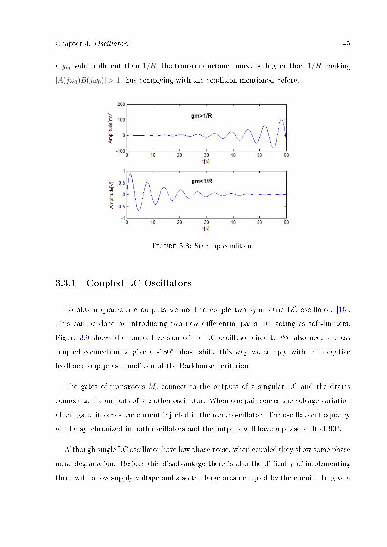
3.3.1 Coupled LC Oscillators
To obtain quadrature outputs we need to couple two symmetric LC oscillator, [15].
This can be done by introducing two new dierential pairs [10] acting as soft-limiters.
Figure 3.9 shows the coupled version of the LC oscillator circuit. We also need a cross
coupled connection to give a -180 phase shift, this way we comply with the negative
feedback loop phase condition of the Barkhausen criterion.
The gates of transistors Mc connect to the outputs of a singular LC and the drains
connect to the outputs of the other oscillator. When one pair senses the voltage variation
at the gate, it varies the current injected in the other oscillator. The oscillation frequency
will be synchronized in both oscillators and the outputs will have a phase shift of 90.
Although single LC oscillator have low phase noise, when coupled they show some phase
noise degradation. Besides this disadvantage there is also the diculty of implementing
them with a low supply voltage and also the large area occupied by the circuit. To give a
Chapter 3. Oscillators 46
I
C
2M1M
1V2V
ddV
CL L
I
C
4M3M
3V4V
CL L
SLI SLI
SLMSLM SLM SLM
Figure 3.9: Coupled LC oscillator circuit.
perspective of how large the circuit is lets say a RC oscillator can occupy the same layout
area as an inductor.
LC oscillators need a strong coupling to be able to synchronize both outputs with a 90.
To increase the coupling, the gates size of the coupling transistors should be increased.
When doing that we are also increasing the parasitics on those transistors, making the
oscillation frequency decrease and degrading the phase noise. Due to this disadvantage
coupled RC oscillators can have similar phase noise performance to that of a LC coupled
oscillator, [10].
3.4 Relaxation Oscillators
RC oscillators have become more important in recent years due to the reduced space
and the improvement of phase noise, when coupled. In this section and the following,
Chapter 3. Oscillators 47
we will discuss two dierent RC oscillators, one with a relaxation (non-linear) behaviour
oscillator and one oscillator with inherent quadrature outputs (Two-Integrator). Initially
we approach the behaviour of those oscillators using ideal blocks, then one basic imple-
mentation to allow a more deep study at circuit level.
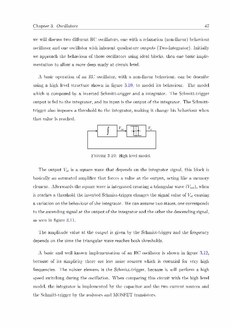
A basic operation of an RC oscillator, with a non-linear behaviour, can be describe
using a high level structure shown in gure 3.10, to model its behaviour. The model
which is composed by a inverted Schmitt-trigger and a integrator. The Schmitt-trigger
output is fed to the integrator, and its input is the output of the integrator. The Schmitt-
trigger also imposes a threshold to the integrator, making it change his behaviour when
that value is reached.
intV stV
Figure 3.10: High level model.
The output Vst is a square wave that depends on the integrator signal, this block is
basically an saturated amplier that forces a value at the output, acting like a memory
element. Afterwards the square wave is integrated creating a triangular wave (Vint), when
it reaches a threshold the inverted Schmitt-trigger changes the signal value of Vst causing
a variation on the behaviour of the integrator. We can assume two states, one corresponds
to the ascending signal at the output of the integrator and the other the descending signal,
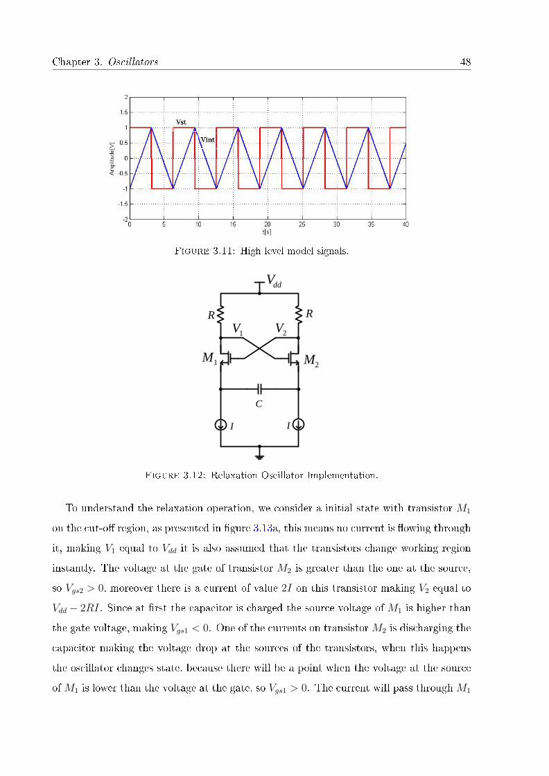
as seen in gure 3.11.
The amplitude value at the output is given by the Schmitt-trigger and the frequency
depends on the time the triangular wave reaches both thresholds.
A basic and well known implementation of an RC oscillator is shown in gure 3.12,
because of its simplicity there are less noise sources which is essential for very high
frequencies. The noisier element is the Schmitt-trigger, because it will perform a high
speed switching during the oscillation. When comparing this circuit with the high level
model, the integrator is implemented by the capacitor and the two current sources and
the Schmitt-trigger by the resistors and MOSFET transistors.
Chapter 3. Oscillators 48
Figure 3.11: High level model signals.
I
ddV
C
RR
I
2M1M
1V 2V
Figure 3.12: Relaxation Oscillator Implementation.
To understand the relaxation operation, we consider a initial state with transistor M1
on the cut-o region, as presented in gure 3.13a, this means no current is owing through
it, making V1 equal to Vdd it is also assumed that the transistors change working region
instantly. The voltage at the gate of transistor M2 is greater than the one at the source,
so Vgs2 > 0, moreover there is a current of value 2I on this transistor making V2 equal to
Vdd − 2RI. Since at rst the capacitor is charged the source voltage of M1 is higher than
the gate voltage, making Vgs1 < 0. One of the currents on transistorM2 is discharging the
capacitor making the voltage drop at the sources of the transistors, when this happens
the oscillator changes state, because there will be a point when the voltage at the source
ofM1 is lower than the voltage at the gate, so Vgs1 > 0. The current will pass throughM1
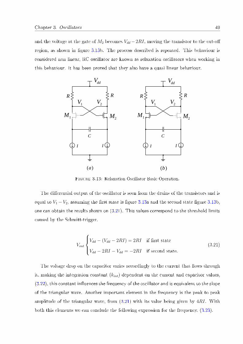
Chapter 3. Oscillators 49
and the voltage at the gate of M2 becomes Vdd−2RI, moving the transistor to the cut-o
region, as shown in gure 3.13b. The process described is repeated. This behaviour is
considered non linear, RC oscillator are known as relaxation oscillators when working in
this behaviour. It has been proved that they also have a quasi linear behaviour.
I
C
RR
I
2M1M
1V 2V
I
C
RR
I
2M1M
1V 2V
ddVddV
)(a )(b
Figure 3.13: Relaxation Oscillator Basic Operation.
The dierential output of the oscillator is seen from the drains of the transistors and is
equal to V1−V2, assuming the rst state is gure 3.13a and the second state gure 3.13b,
one can obtain the results shown on (3.21). This values correspond to the threshold limits
caused by the Schmitt-trigger.
Vout
Vdd − (Vdd − 2RI) = 2RI if rst state
Vdd − 2RI − Vdd = −2RI if second state.
(3.21)
The voltage drop on the capacitor varies accordingly to the current that ows through
it, making the integration constant (kint) dependent on the current and capacitor values,
(3.22), this constant inuences the frequency of the oscillator and is equivalent to the slope
of the triangular wave. Another important element in the frequency is the peak to peak
amplitude of the triangular wave, from (3.21) with its value being given by 4RI. With
both this elements we can conclude the following expression for the frequency, (3.23).
Chapter 3. Oscillators 50
kint =I
C(3.22)
f0 =I
2C(4RI)=
1
8RC(3.23)
Transistors M1 and M2 don't switch between the cut-o region and the saturation
region instantly. There is a period of time where the transistors act as resistors (triode
region), which is one of the noise sources of the circuit. At higher frequencies, reduced C
value, the transistor parasitics will inuence the Schmitt-trigger input impedance. Instead
of having just a real part there is also a positive imaginary equivalent to a inductor. The
imaginary part is then canceled by the capacitor impedance, making the oscillator have a
quasi linear behaviour, [2], where the Barkhausen conditions apply. With this behaviour
instead of having a square wave at the output (relaxation oscillator) the oscillator will
have a sinusoidal signal.
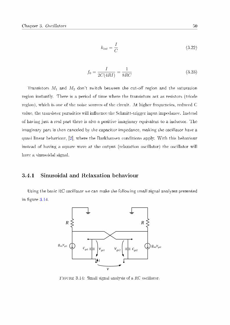
3.4.1 Sinusoidal and Relaxation behaviour
Using the basic RC oscillator we can make the following small signal analyses presented
in gure 3.14.
R R
i
v
11 gsm vg22 gsm vg
1gsc2gsc1gsv 2gsv
Figure 3.14: Small signal analysis of a RC oscillator.
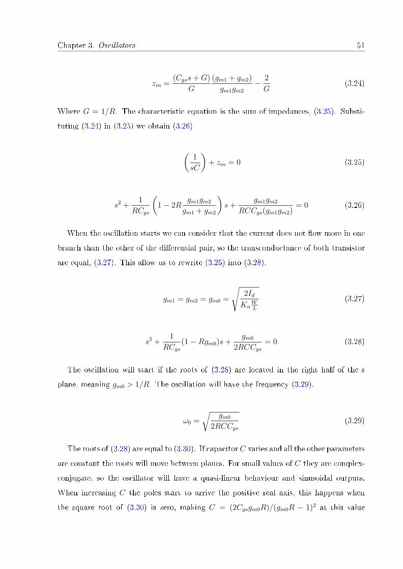
Chapter 3. Oscillators 51
zin =(Cgss+G)
G
(gm1 + gm2)
gm1gm2
− 2
G(3.24)
Where G = 1/R. The characteristic equation is the sum of impedances, (3.25). Substi-
tuting (3.24) in (3.25) we obtain (3.26)
(1
sC
)+ zin = 0 (3.25)
s2 +1
RCgs
(1− 2R
gm1gm2
gm1 + gm2
)s+
gm1gm2
RCCgs(gm1gm2)= 0 (3.26)
When the oscillation starts we can consider that the current does not ow more in one
branch than the other of the dierential pair, so the transconductance of both transistor
are equal, (3.27). This allow us to rewrite (3.25) into (3.28).
gm1 = gm2 = gm0 =
√2Id
KnWL
(3.27)
s2 +1
RCgs(1−Rgm0)s+
gm0
2RCCgs= 0 (3.28)
The oscillation will start if the roots of (3.28) are located in the right half of the s
plane, meaning gm0 > 1/R. The oscillation will have the frequency (3.29).
ω0 =
√gm0
2RCCgs(3.29)
The roots of (3.28) are equal to (3.30). If capacitor C varies and all the other parameters
are constant the roots will move between planes. For small values of C they are complex-
conjugate, so the oscillator will have a quasi-linear behaviour and sinusoidal outputs.
When increasing C the poles start to arrive the positive real axis, this happens when
the square root of (3.30) is zero, making C = (2Cgsgm0R)/(gm0R − 1)2 at this value
Chapter 3. Oscillators 52
the oscillator starts to have a non linear behaviour. With further increase of C the
roots are moving along the positive real axis arriving to the nal values of s1 = 0 and
s2 = (Rgm0−1)/(RCgs). The transition from one type of behaviour to another is smooth,
it represents a gradual increase of distortions on the sinusoidal wave, then the oscillations
start to have a square waveform, just like relaxation oscillators.
s1,2 =gm0R− 1
2RCgs±
√(gm0R− 1
2RCgs
)2
− gm0
2RCCgs(3.30)
Before moving into the oscillation dierential equation we need to do the following
approximation, (3.31), where i is the capacitor current. Then, we can write for this
current the dierential equation (3.32). Introducing the normalized variable x = i/(√
2I)
and notations δ0 = (Rgm0 − 1)/(2RCgs) and δ2 = gm0/(2Cgs) the equation is reduced to
(3.33).
gm1gm2
gm1 + gm2
≈ gm0
2
[1−
(i√2I
)2]
(3.31)
d2
dt2+
1
RCgs
(1−Rgm0
[1−
(i√2I
)2])
d
dt+ ω2
0i = 0 (3.32)
d2x
dt2− 2(δ0 − δ2x
2)dx
dt+ ω2
0x = 0 (3.33)
The solution to (3.33) is (3.34). The amplitude of the voltage between the drain resistor
will be (3.35).
x = 2
√δ0
δ2
sin f0t = 2
√1−
(1
Rgm0
)sin f0t (3.34)
Vdm = 4√
2I
√1−
(1
Rgm0
)(3.35)
Chapter 3. Oscillators 53
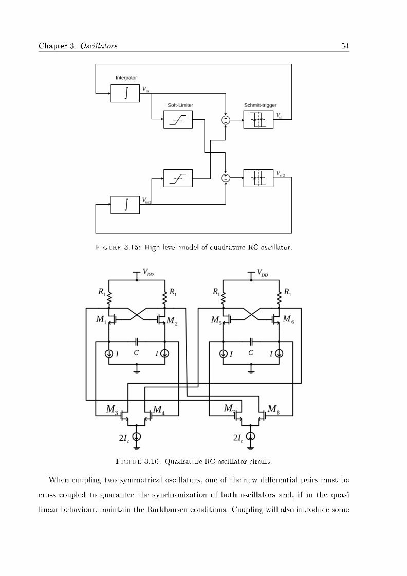
3.4.2 Coupled RC oscillators
Like LC oscillators, to obtain quadrature outputs we need to connect two symmetrical
RC oscillators. The connection is made using a soft-limiter at the output of the integrator,
if we increase its gain then we will obtain a square wave signal at the output. Unlike the
Schmitt-trigger that only changes when a threshold is reached, the soft-limiter saturates
when the triangular wave goes above zero. This way we obtain a square wave with a 90
dierence from the Schmitt-trigger output.
Figure 3.15 shows a high level block diagram of the coupled RC oscillator. The output
of the soft-limiter is used to synchronize the other RC oscillator. Its square signal is added
to the triangular output signal of the other integrator, then this new signal goes to the
Schmitt-trigger creating a feedback structure. This way both outputs have always a 90
phase shift and the same frequency.
The resulting wave of the signal addition, assumes a important part on the overall
noise. This signal as a steeper slope and denes each oscillator state transitions, which
means the switching times are less sensitive to noise [10]. As mentioned, the higher the
gain of the soft-limiter the more square the output becomes, and thus, increasing the
slope, making the oscillator less sensitive to noise.
At circuit level the soft-limiter is implemented by a dierential pair, shown on gure
3.16. This coupling method as the same features as the one presented on the LC oscillators,
but in this case the gates are connected to the capacitor terminals. When the voltage
at the gate varies, the current on the other oscillator also changes. To see the how it
inuences the output amplitude, lets analyse one of the oscillators when transistor M1 is
o and M2 is on. As we seen before the M1 would have a voltage equal to Vdd and the M2
branch Vdd − 4RI, but in a coupled version the outputs will be (3.36), with the current
isl1 lower than isl2.
v1 = Vdd − isl1R
v2 = Vdd − 2RI − isl2R(3.36)
Chapter 3. Oscillators 54
intV
stV
2intV
2stV
Integrator
Soft-Limiter Schmitt-trigger
Figure 3.15: High level model of quadrature RC oscillator.
ICI
1M2M
1R
DDV
1R
ICI
5M 6M
1R
DDV
1R
cI2
8M7M
cI2
3M4M
Figure 3.16: Quadrature RC oscillator circuit.
When coupling two symmetrical oscillators, one of the new dierential pairs must be
cross coupled to guarantee the synchronization of both oscillators and, if in the quasi
linear behaviour, maintain the Barkhausen conditions. Coupling will also introduce some
Chapter 3. Oscillators 55
changes in the single RC oscillator performance. It adds new noise sources due to the new
active elements, but the advantages given are superior. The phase noise improves, but on
the other hand, the frequency is reduced.
The supply voltage is decreasing this combine with the need to use low power circuits.
From (3.36) we can see how troublesome it will become for implementing coupled oscilla-
tors, by introducing new dierential pairs we need to be careful about the supply voltage.
Some new coupling techniques have been developed to solve this problem. Instead of using
a current and a dierential pair, the coupling is made using capacitors, this reduces not
only the power consumption but also some noise sources.
In recent years coupled RC oscillators have become the subject of many studies, due
to the good performance, low area, and quadrature outputs. Coupled LC oscillators have
the same performance as RC but occupy a larger area. As mentioned many times the goal
is to attain a single chip transceiver, this oscillator type combined with CMOS technology
allows that. Many RC architectures have been developed and some are being restudied
with the goal to reduce power consumption, improve phase noise and increase tunning
frequency.
3.5 Two-Integrator Oscillator
The Two-Integrator oscillator unlike the previous ones, generates quadrature outputs
without the need of a coupling circuit, but as a result it only works with quadrature
outputs. Although the operation is similar to RC oscillators the structure is dierent, the
Schmitt-trigger is substituted by another integrator.
At a high level model the two integrator oscillator can be seen as two stages, each
with an ideal integrator and a amplier. These two stages are in cascade, and the output
of the second stage is inverted and fed back to the rst stage, as shown on gure 3.17.
Depending on the amplier, the oscillator has two types of behaviour, non linear and
quasi-linear [10, 27].
Chapter 3. Oscillators 56
1
1 21G 2G
Figure 3.17: High level study of two integrator oscillator.
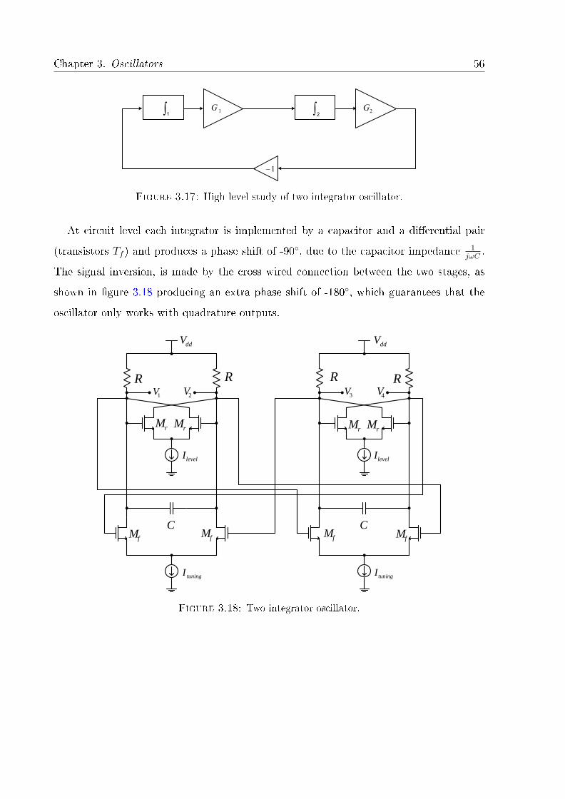
At circuit level each integrator is implemented by a capacitor and a dierential pair
(transistors Tf ) and produces a phase shift of -90, due to the capacitor impedance 1jωC
.
The signal inversion, is made by the cross wired connection between the two stages, as
shown in gure 3.18 producing an extra phase shift of -180, which guarantees that the
oscillator only works with quadrature outputs.
rM
fM
levelI levelI
tuningI tuningI
ddV ddV
C C
1V 2V 3V4V
RR R R
rMrM rM
fM fMfM
Figure 3.18: Two integrator oscillator.
Chapter 3. Oscillators 57
3.5.1 Non Linear behaviour
3.5.1.1 High Level Study
For the oscillator to have a non linear behaviour, the dierential pair made by transis-
tors Tr must be in the saturation region of gure 3.20. When increasing the current Ilevel,
the transconductance gm = 2IdVdsat
also increases, making the slope steeper and saturating
the outputs more easily, (3.37). In the saturation state the output will form a square
wave, depending on the value of the input signal (if it is positive or negative). Then the
square wave is integrated resulting on a triangular wave. This behaviour is similar to the
one seen on a relaxation oscillator.
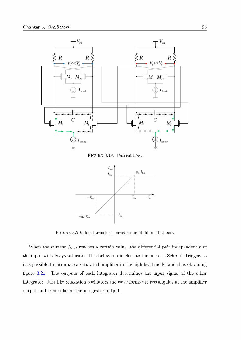
The lower dierential pair determines in which way the current ows through the
capacitor, depending on the voltage at his terminals. Transistors Tf will change their
working regions, depending on the signal at the gate. In theory both transistor work as
a switch, when one is open the other is closed, so all the current ows through the latter
one. In reality both transistors are conducting, as shown on gure 3.19, but there is more
current in one of them.
Since the current is always changing, the capacitor is charging in dierent directions
repeatedly thus creating the oscillation frequency, given by (3.38). The upper dierential
pair has the same behaviour delivering −Ilim and Ilim with a 50 % duty cycle. In this
case the oscillator amplitude is (3.39).
Iout(Vin)
Ilim = gmVlim if Vin ≥ Vlim,
gmVin if − Vlim < Vin < Vlim,
−Ilim = −gmVlim if Vin ≤ −Vlim.
(3.37)
ω0 =Ituning2CVout
(3.38)
Vout = RIlevel (3.39)
Chapter 3. Oscillators 58
tuningI tuningI
ddV ddV
C C
1V 2V 3V4V
fM
R R R R
fM fMfM
levelI levelI
rMrM
rM rM
Figure 3.19: Current ow.
outI
inVlimV
limI
limV
limI
limVgm
limVgm
Figure 3.20: Ideal transfer characteristic of dierential pair.
When the current Ilevel reaches a certain value, the dierential pair independently of
the input will always saturate. This behaviour is close to the one of a Schmitt Trigger, so
it is possible to introduce a saturated amplier in the high level model and thus obtaining
gure 3.21. The outputs of each integrator determines the input signal of the other
integrator. Just like relaxation oscillators the wave forms are rectangular at the amplier
output and triangular at the integrator output.
Chapter 3. Oscillators 59
1
1 1 2 2
Figure 3.21: High Level model for the Two-Integrator oscillator with non linear be-
haviour.
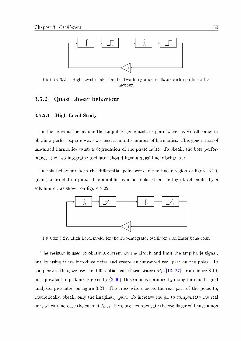
3.5.2 Quasi Linear behaviour
3.5.2.1 High Level Study
In the previous behaviour the amplier generated a square wave, as we all know to
obtain a perfect square wave we need a innite number of harmonics. This generation of
unwanted harmonics cause a degradation of the phase noise. To obtain the best perfor-
mance, the two integrator oscillator should have a quasi linear behaviour.
In this behaviour both the dierential pairs work in the linear region of gure 3.20,
giving sinusoidal outputs. The amplier can be replaced in the high level model by a
soft-limiter, as shown on gure 3.22.
1
1 1 2 2
Figure 3.22: High Level model for the Two-Integrator oscillator with linear behaviour.
The resistor is used to obtain a current on the circuit and limit the amplitude signal,
but by using it we introduce noise and create an unwanted real part on the poles. To
compensate that, we use the dierential pair of transistors Mr ([10, 27]) from gure 3.19,
his equivalent impedance is given by (3.40), this value is obtained by doing the small signal
analysis, presented on gure 3.23. The cross wire cancels the real part of the poles to,
theoretically, obtain only the imaginary part. To increase the gm to compensate the real
part we can increase the current Ilevel. If we over-compensate the oscillator will have a non

Chapter 3. Oscillators 60
linear behaviour, on the other hand, if a balanced compensation is made the dierential
pair avoids saturation.
rx =vxix
= − 2
gm(3.40)
↓ ↓
2xv
2xv
2
gmvx
2
gmvx
xi
xv
Figure 3.23: Small signal analysis of dierential pair.
Observing the small signal analysis of a transconductance one can see that is equivalent
to a slope as shown on (3.41). The vgs of transistor Tr is always changing and therefore
the gm also changes, as seen in gure 3.24. As mentioned before the role of this transcon-
ductance is to cancel the real part caused by the resistors, since their value is always
changing, the poles will move between the stable and unstable region. This is one of the
noise source that contribute to the phase noise, since in reality it is impossible to obtain
a constant frequency at the output.
gm =∂id∂vgs
(3.41)
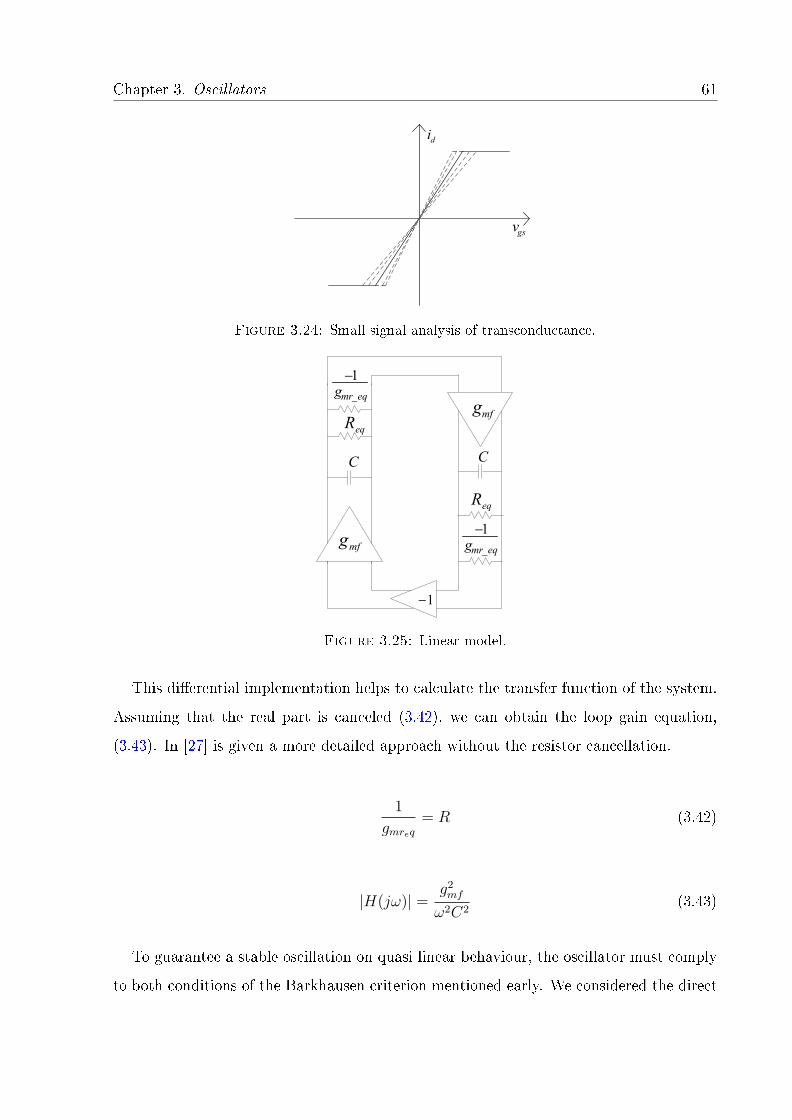
Figure 3.25 represents a practical approach of the two-integrator in the linear operation.
Resistors Req model all the resistors in one stage and also represents any losses in the
circuit.
Chapter 3. Oscillators 61
di
gsv
Figure 3.24: Small signal analysis of transconductance.
1
mfg
C C
mfg
eqR
eqmrg _
1
eqR
eqmrg _
1
Figure 3.25: Linear model.
This dierential implementation helps to calculate the transfer function of the system.
Assuming that the real part is canceled (3.42), we can obtain the loop gain equation,
(3.43). In [27] is given a more detailed approach without the resistor cancellation.
1
gmreq= R (3.42)
|H(jω)| =g2mf
ω2C2(3.43)
To guarantee a stable oscillation on quasi linear behaviour, the oscillator must comply
to both conditions of the Barkhausen criterion mentioned early. We considered the direct
Chapter 3. Oscillators 62
coupling, meaning a positive feedback, so the second condition says the phase shift must
be equal to a multiple of 360, Equation 3.5. Each capacitor creates a phase shift of 90,
since we have two, the total will be 180, there is also a signal inversion block that adds
a phase shift of 180. This complies to the second condition of the criterion.
The oscillation frequency is obtained by applying the Barkhausen condition,(3.44).
Through the equation one can conclude that there are two ways of changing the value of
the frequency, one is changing the capacitor value and the other the current Ituning that
consequently changes the transconductance of the transistor Tf . If the capacitor value is
too low, the parasitic capacitors of the transistors will inuence the frequency, making
the value of the capacitor higher and thus lowering the frequency.
ω =gmfC
(3.44)
Assuming that the current in the dierential pair is equal to the source current the
oscillator amplitude is given by (3.45). When working with a non linear behaviour we will
have the maximum output amplitude possible. In the linear behaviour the amplitude is
limited by the slope of the amplier. To achieve a optimum point, the current Ilevel must
be close to saturation, [27]. But this brings some disadvantages, the power consumption
increases and the FOM worsens and there is the risk of entering the non linear region.
Vout = RIlevel (3.45)
Chapter 4
Circuit Design and Implementation
This is the main chapter of this thesis. We will present the designed RC oscillators cir-
cuits and their simulation results. The rst two are relaxation oscillators implementations
and the last circuit is a ring oscillator (Two-Integrator).
The rst circuit shows a wideband MOS quadrature oscillator with two coupled relax-
ation oscillators, also called multivibrators. Two dierent forms of coupling (soft and hard)
are implemented and compared. We investigated the inuence of capacitor and current
mismatches in quadrature errors. In the last part we will analyse how the multivibrator
locks with a external synchronizing harmonic.
The second circuit is a simple RC oscillator with some circuit modications, based on
known techniques and a new method for reducing the phase noise. The inuence of each
technique will also be discussed.
The last circuit is a fully integrated CMOS two-integrator with low area and power
consumption. The design of some components in CMOS will be discussed. The layout of
the circuit in a 130 nm technology is also presented.
63
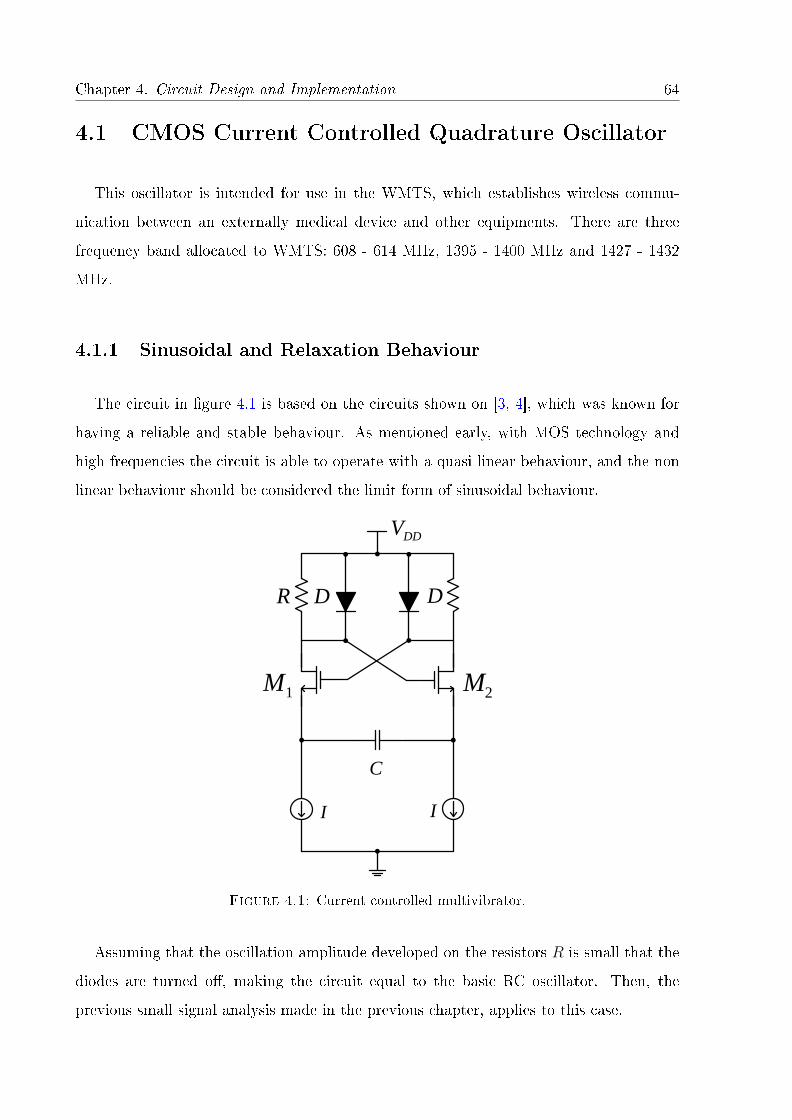
Chapter 4. Circuit Design and Implementation 64
4.1 CMOS Current Controlled Quadrature Oscillator
This oscillator is intended for use in the WMTS, which establishes wireless commu-
nication between an externally medical device and other equipments. There are three
frequency band allocated to WMTS: 608 - 614 MHz, 1395 - 1400 MHz and 1427 - 1432
MHz.
4.1.1 Sinusoidal and Relaxation Behaviour
The circuit in gure 4.1 is based on the circuits shown on [3, 4], which was known for
having a reliable and stable behaviour. As mentioned early, with MOS technology and
high frequencies the circuit is able to operate with a quasi linear behaviour, and the non
linear behaviour should be considered the limit form of sinusoidal behaviour.
I
DDV
C
R
I
D D
1M 2M
Figure 4.1: Current controlled multivibrator.
Assuming that the oscillation amplitude developed on the resistors R is small that the
diodes are turned o, making the circuit equal to the basic RC oscillator. Then, the
previous small signal analysis made in the previous chapter, applies to this case.
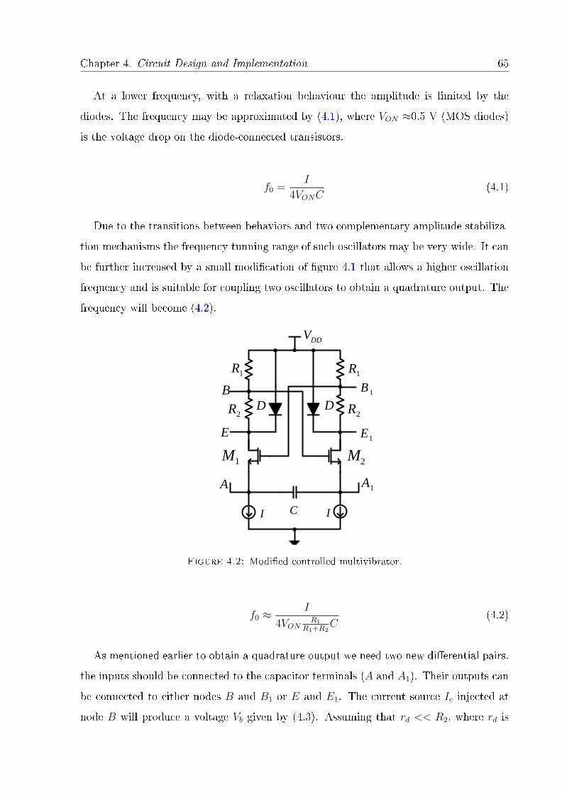
Chapter 4. Circuit Design and Implementation 65
At a lower frequency, with a relaxation behaviour the amplitude is limited by the
diodes. The frequency may be approximated by (4.1), where VON ≈0.5 V (MOS diodes)
is the voltage drop on the diode-connected transistors.
f0 =I
4VONC(4.1)
Due to the transitions between behaviors and two complementary amplitude stabiliza-
tion mechanisms the frequency tunning range of such oscillators may be very wide. It can
be further increased by a small modication of gure 4.1 that allows a higher oscillation
frequency and is suitable for coupling two oscillators to obtain a quadrature output. The
frequency will become (4.2).
ICI
D D2R
1R
DDV
B 1B
1E
1A
E
A
2R
1R
1M 2M
Figure 4.2: Modied controlled multivibrator.
f0 ≈I
4VONR1
R1+R2C
(4.2)
As mentioned earlier to obtain a quadrature output we need two new dierential pairs.
the inputs should be connected to the capacitor terminals (A and A1). Their outputs can
be connected to either nodes B and B1 or E and E1. The current source Ic injected at
node B will produce a voltage Vb given by (4.3). Assuming that rd << R2, where rd is
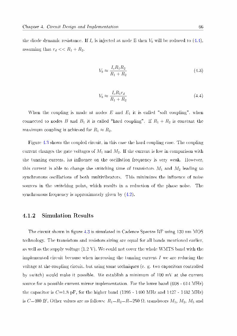
Chapter 4. Circuit Design and Implementation 66
the diode dynamic resistance. If Ic is injected at node E then Vb will be reduced to (4.4),
assuming that rd << R1 +R2.
Vb ≈IcR1R2
R1 +R2
(4.3)
Vb ≈IcR1rdR1 +R2
(4.4)
When the coupling is made at nodes E and E1 it is called "soft coupling", when
connected to nodes B and B1 it is called "hard coupling". If R1 + R2 is constant the
maximum coupling is achieved for R1 ≈ R2.
Figure 4.3 shows the coupled circuit, in this case the hard coupling case. The coupling
current changes the gate voltages of M1 and M2. If the current is low in comparison with
the tunning current, its inuence on the oscillation frequency is very weak. However,
this current is able to change the switching time of transistors M1 and M2 leading to
synchronous oscillations of both multivibrators. This minimizes the inuence of noise
sources in the switching point, which results in a reduction of the phase noise. The
synchronous frequency is approximately given by (4.2).
4.1.2 Simulation Results
The circuit shown in gure 4.3 is simulated in Cadence Spectre RF using 130 nm MOS
technology. The transistors and resistors sizing are equal for all bands mentioned earlier,
as well as the supply voltage (1.2 V). We could not cover the whole WMTS band with the
implemented circuit because when increasing the tunning current I we are reducing the
voltage at the coupling circuit, but using some techniques (e. g. two capacitors controlled
by switch) would make it possible. We establish a minimum of 100 mV at the current
source for a possible current mirror implementation. For the lower band (608 - 614 MHz)
the capacitor is C=1.8 pF, for the higher band (1395 - 1400 MHz and 1427 - 1432 MHz)
is C=400 fF. Other values are as follows: R1=R2=R=250 Ω, transistors M1, M2, M5 and
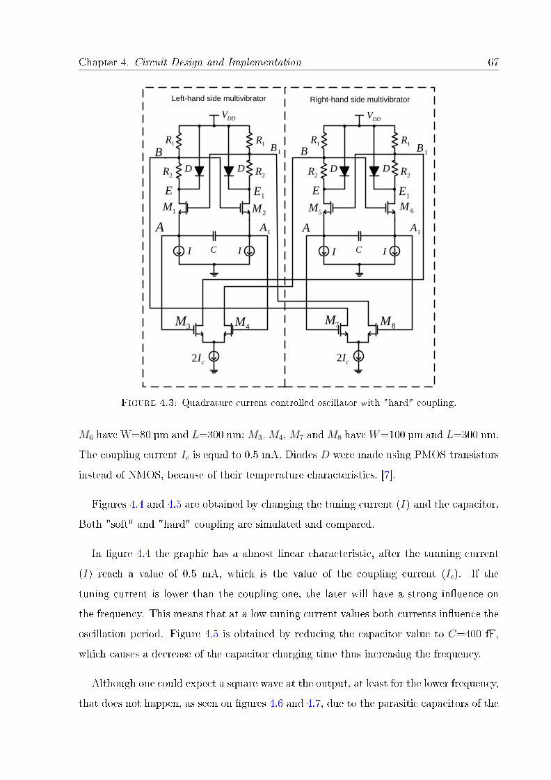
Chapter 4. Circuit Design and Implementation 67
ICI
D D
1M2M
2R
1R
DDV
B 1B
1E
1A
E
A
2R
1R
ICI
D D
5M 6M
2R
1R
DDV
B 1B
1E
1A
E
A
2R
1R
cI2
8M7M
Left-hand side multivibrator Right-hand side multivibrator
cI2
3M4M
Figure 4.3: Quadrature current controlled oscillator with "hard" coupling.
M6 have W=80 µm and L=300 nm;M3,M4,M7 andM8 haveW=100 µm and L=300 nm.
The coupling current Ic is equal to 0.5 mA. Diodes D were made using PMOS transistors
instead of NMOS, because of their temperature characteristics, [7].
Figures 4.4 and 4.5 are obtained by changing the tuning current (I) and the capacitor.
Both "soft" and "hard" coupling are simulated and compared.
In gure 4.4 the graphic has a almost linear characteristic, after the tunning current
(I) reach a value of 0.5 mA, which is the value of the coupling current (Ic). If the
tuning current is lower than the coupling one, the later will have a strong inuence on
the frequency. This means that at a low tuning current values both currents inuence the
oscillation period. Figure 4.5 is obtained by reducing the capacitor value to C=400 fF,
which causes a decrease of the capacitor charging time thus increasing the frequency.
Although one could expect a square wave at the output, at least for the lower frequency,
that does not happen, as seen on gures 4.6 and 4.7, due to the parasitic capacitors of the
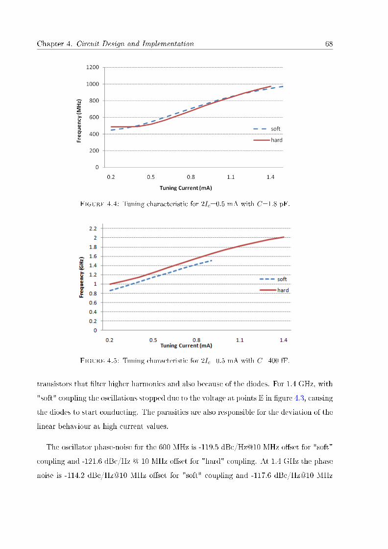
Chapter 4. Circuit Design and Implementation 68
Figure 4.4: Tuning characteristic for 2Ic=0.5 mA with C=1.8 pF.
Figure 4.5: Tuning characteristic for 2Ic=0.5 mA with C=400 fF.
transistors that lter higher harmonics and also because of the diodes. For 1.4 GHz, with
"soft" coupling the oscillations stopped due to the voltage at points E in gure 4.3, causing
the diodes to start conducting. The parasitics are also responsible for the deviation of the
linear behaviour at high current values.
The oscillator phase-noise for the 600 MHz is -119.5 dBc/Hz@10 MHz oset for "soft"
coupling and -121.6 dBc/Hz @ 10 MHz oset for "hard" coupling. At 1.4 GHz the phase
noise is -114.2 dBc/Hz@10 MHz oset for "soft" coupling and -117.6 dBc/Hz@10 MHz
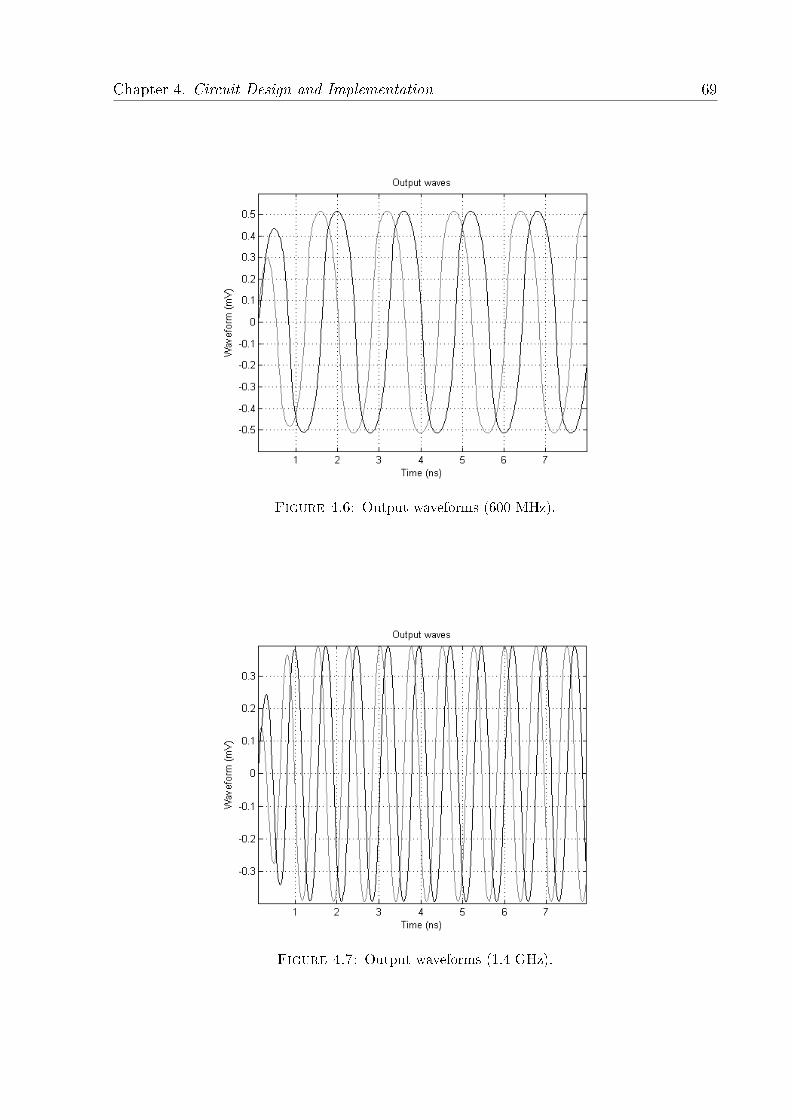
Chapter 4. Circuit Design and Implementation 69
Figure 4.6: Output waveforms (600 MHz).
Figure 4.7: Output waveforms (1.4 GHz).
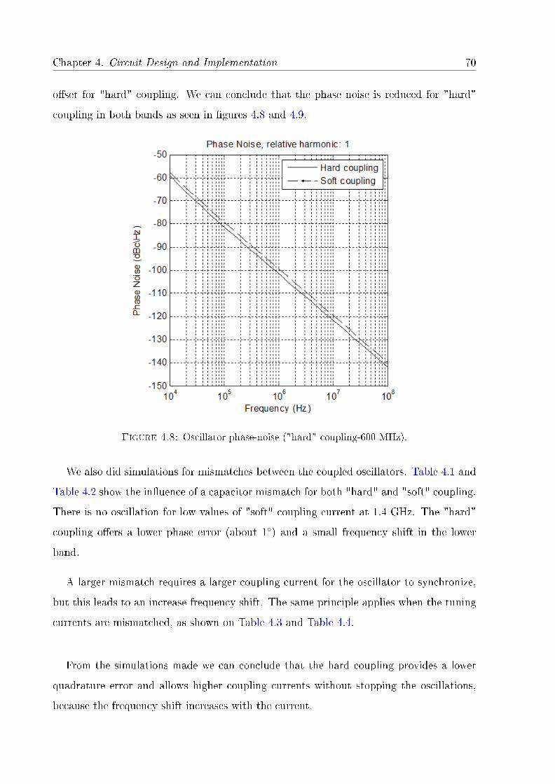
Chapter 4. Circuit Design and Implementation 70
oset for "hard" coupling. We can conclude that the phase noise is reduced for "hard"
coupling in both bands as seen in gures 4.8 and 4.9.
Figure 4.8: Oscillator phase-noise ("hard" coupling-600 MHz).
We also did simulations for mismatches between the coupled oscillators. Table 4.1 and
Table 4.2 show the inuence of a capacitor mismatch for both "hard" and "soft" coupling.
There is no oscillation for low values of "soft" coupling current at 1.4 GHz. The "hard"
coupling oers a lower phase error (about 1) and a small frequency shift in the lower
band.
A larger mismatch requires a larger coupling current for the oscillator to synchronize,
but this leads to an increase frequency shift. The same principle applies when the tuning
currents are mismatched, as shown on Table 4.3 and Table 4.4.
From the simulations made we can conclude that the hard coupling provides a lower
quadrature error and allows higher coupling currents without stopping the oscillations,
because the frequency shift increases with the current.
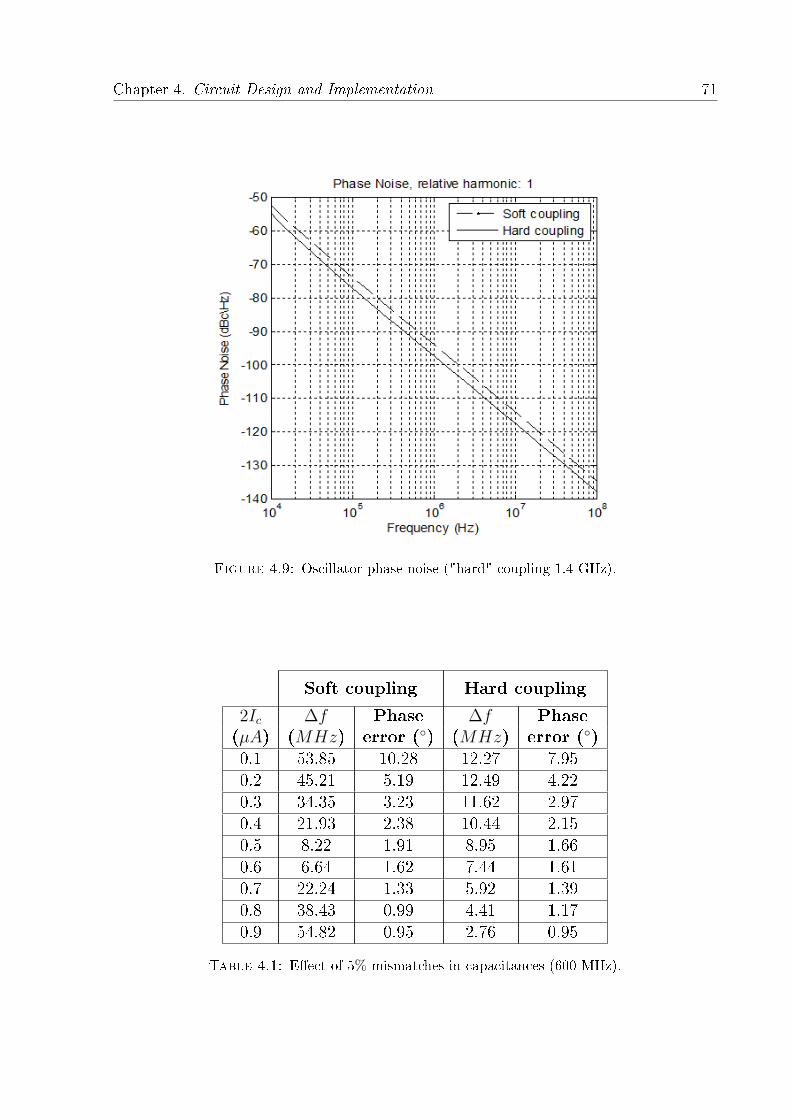
Chapter 4. Circuit Design and Implementation 71
Figure 4.9: Oscillator phase-noise ("hard" coupling-1.4 GHz).
Soft coupling Hard coupling
2Ic ∆f Phase ∆f Phase(µA) (MHz) error () (MHz) error ()0.1 53.85 10.28 12.27 7.950.2 45.21 5.19 12.49 4.220.3 34.35 3.23 11.62 2.970.4 21.93 2.38 10.44 2.150.5 8.22 1.91 8.95 1.660.6 6.64 1.62 7.44 1.610.7 22.24 1.33 5.92 1.390.8 38.43 0.99 4.41 1.170.9 54.82 0.95 2.76 0.95
Table 4.1: Eect of 5% mismatches in capacitances (600 MHz).

Chapter 4. Circuit Design and Implementation 72
Soft coupling Hard coupling
2Ic ∆f Phase ∆f Phase(µA) (MHz) error () (MHz) error ()0.1 No Oscillation 71.86 1.450.2 No Oscillation 59.49 1.590.3 25.19 0.92 46.28 1.090.4 20.87 0.86 32.12 0.760.5 13.43 0.84 17.33 0.570.6 3.56 0.93 2.33 0.40.7 8.16 1.02 12.54 0.340.8 21.03 1.09 26.96 0.330.9 34.51 1.2 40.74 0.29
Table 4.2: Eect of 5% mismatches in capacitances (1.4 GHz).
Soft coupling Hard coupling
2Ic ∆f Phase ∆f Phase(µA) (MHz) error () (MHz) error ()0.1 36.34 10.82 5.81 7.860.2 27.96 5.47 5.94 4.030.3 16.77 3.65 5.46 3.350.4 4.41 2.71 8.69 2.090.5 9.29 2.21 10.49 1.740.6 24.13 1.88 12.17 1.430.7 39.66 1.71 14.03 1.20.8 55.85 1.47 15.63 1.050.9 72.04 1.52 17.33 0.96
Table 4.3: Eect of 5% mismatches in tuning currents (600 MHz).
4.1.3 Frequency Locking
We also investigated frequency locking when a external current source is applied be-
tween nodes B and B1, as shown on gure 4.10. A single oscillator at 600 MHz can be
synchronized by a current source with an amplitude of 100 µA, as seen on gure 4.11.
Because of the dierential output we only have odd harmonics, that why the locking is
only possible for those harmonics.
It is possible to lock the oscillator up to the 11th sub-harmonic frequency, as shown
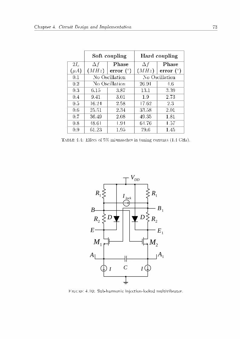
Chapter 4. Circuit Design and Implementation 73
Soft coupling Hard coupling
2Ic ∆f Phase ∆f Phase(µA) (MHz) error () (MHz) error ()0.1 No Oscillation No Oscillation0.2 No Oscillation 26.91 4.60.3 6.15 3.87 13.1 3.390.4 9.41 3.01 1.9 2.730.5 16.24 2.58 17.62 2.30.6 25.51 2.34 33.58 2.010.7 36.49 2.08 49.35 1.810.8 48.61 1.94 64.76 1.570.9 61.23 1.95 79.6 1.45
Table 4.4: Eect of 5% mismatches in tuning currents (1.4 GHz).
ICI
D D
1M2M
2R
1R
B 1B
1E
1A
E
A
2R
1RlockI
DDV
Figure 4.10: Sub-harmonic injection-locked multivibrator.
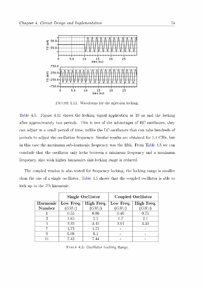
Chapter 4. Circuit Design and Implementation 74
Figure 4.11: Waveforms for the injection locking.
Table 4.5. Figure 4.11 shows the locking signal application at 10 ns and the locking
after approximately two periods. This is one of the advantages of RC oscillators, they
can adjust in a small period of time, unlike the LC oscillators that can take hundreds of
periods to adjust the oscillation frequency. Similar results are obtained for 1.4 GHz, but
in this case the maximum sub-harmonic frequency was the fth. From Table 4.5 we can
conclude that the oscillator only locks between a minimum frequency and a maximum
frequency, also with higher harmonics this locking range is reduced.
The coupled version is also tested for frequency locking, the locking range is smaller
than the one of a single oscillator. Table 4.5 shows that the coupled oscillator is able to
lock up to the 5th harmonic.
Single Oscillator Coupled Oscillator
Harmonic Low Freq. High Freq. Low Freq. High Freq.Number (GHz) (GHz) (GHz) (GHz)
1 0.55 0.86 0.46 0.753 1.85 2.2 1.7 2.15 3.33 3.45 3.04 3.337 4.73 4.75 - -9 6.08 6.1 - -11 7.43 7.44 - -
Table 4.5: Oscillator Locking Range.
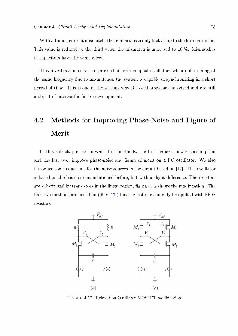
Chapter 4. Circuit Design and Implementation 75
With a tuning current mismatch, the oscillator can only lock at up to the fth harmonic.
This value is reduced to the third when the mismatch is increased to 10 %. Mismatches
in capacitors have the same eect.
This investigation serves to prove that both coupled oscillators when not running at
the same frequency due to mismatches, the system is capable of synchronizing in a short
period of time. This is one of the reasons why RC oscillators have survived and are still
a object of interest for future development.
4.2 Methods for Improving Phase-Noise and Figure of
Merit
In this sub chapter we present three methods, the rst reduces power consumption
and the last two, improve phase-noise and gure of merit on a RC oscillator. We also
introduce some equations for the noise sources in the circuit based on [17]. This oscillator
is based on the basic circuit mentioned before, but with a slight dierence. The resistors
are substituted by transistors in the linear region, gure 4.12 shows the modication. The
rst two methods are based on ([6] e [17]) but the last one can only be applied with MOS
resistors.
I
C
RR
I
2M1M
1V 2V
I
C
I
2M1M
1V 2V
ddV ddV
)(a )(b
3V 3V3M 4M
Figure 4.12: Relaxation Oscillator MOSFET modication.
Chapter 4. Circuit Design and Implementation 76
4.2.1 Pulse Self Biasing
A disadvantage of the RC oscillator is the two current sources, seen on gure 4.12.
This issue aects the power consumption and degrades the FOM. This application of this
method on our circuit, reduces the power to half but increases the thermal noise on the
circuit. In [17] it has been proved that when the current pulse width is small, the phase
noise of the circuit is reduced.
The 1/∆ω2 component of phase-noise is deeply inuenced by the thermal noise from
the components of the circuit. Equation (4.5) from [17], is a simplied modication of
the phase-noise equation representing that inuence. The thermal noise power spectral
density ofM1, the current mirror and circuit losses is equivalent to (i2n,M1/∆f), (i2n,tail/∆f)
and (i2n,Rp/∆f) respectively; ΓM1, Γtail and ΓRp are the root mean square values of their
impulse sensitivity function.
L(∆ω) = 10 log
(i2n,Rp
∆f
)Γ2Rp +
(i2n,M1
∆f
)Γ2M1 +
(i2n,tail
∆f
)Γ2tail
2V 2maxC
2T (∆ω)2
(4.5)
When the tail current is constant, the thermal noise from the oscillator losses is
i2n,Rp/∆f = 4kT/Rp. The thermal noise spectral density of M1 is i2n,M1/∆f = 4kTγξ/Rp
where ξ = gm0Rp, gm0 represents the transconductance of M1. Finally the tail current
thermal noise is given by i2n,tail/∆f = 4kTγ/Rp√
2η0, where η0 is the ratio of the size
between transistor M1 and the tail device. Since the current is constant the impulse
sensitivity function is also constant. By substituting all elements in (4.5) we get (4.6).
L(∆ω) = 10 log
(kT (1 + 1
2γξ + 1
2γξ√
2η0)(2π
)2Rp3I2C2
T (∆ω)2
)(4.6)
With a pulsed tailed current (4.7) with a duration of 2Φ in radians, where φ is the
oscillator phase (φ = ω0t) and Ip is the peak value, each component of (4.5) will change.
The thermal noise ofM1 will become (4.8), but in this case the impulse sensitivity function
will be (4.9).
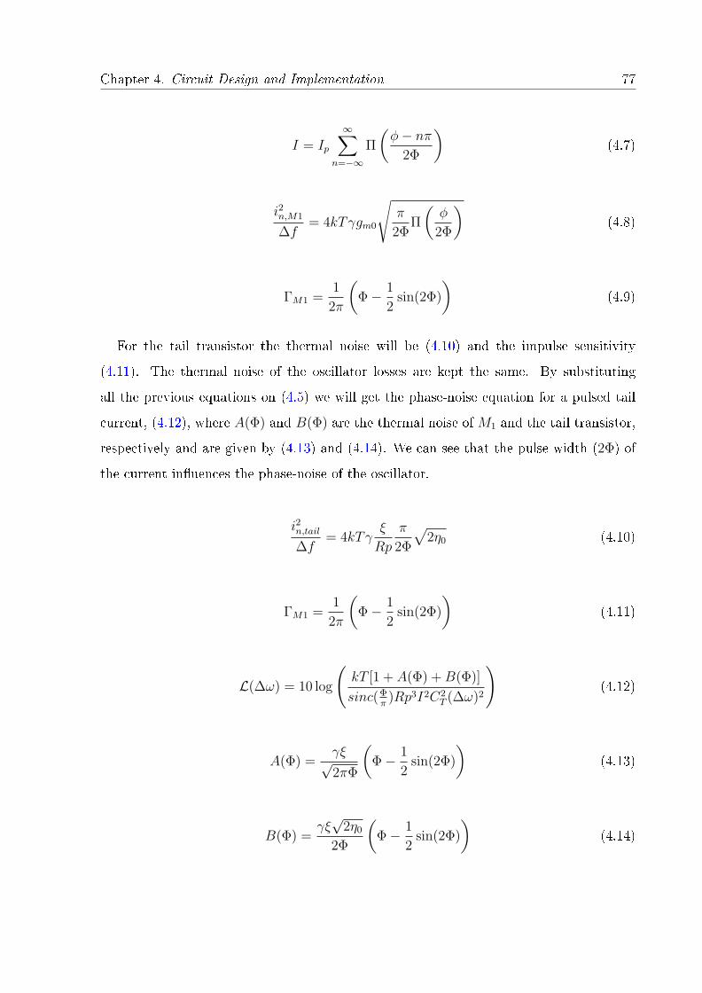
Chapter 4. Circuit Design and Implementation 77
I = Ip
∞∑n=−∞
Π
(φ− nπ
2Φ
)(4.7)
i2n,M1
∆f= 4kTγgm0
√π
2ΦΠ
(φ
2Φ
)(4.8)
ΓM1 =1
2π
(Φ− 1
2sin(2Φ)
)(4.9)
For the tail transistor the thermal noise will be (4.10) and the impulse sensitivity
(4.11). The thermal noise of the oscillator losses are kept the same. By substituting
all the previous equations on (4.5) we will get the phase-noise equation for a pulsed tail
current, (4.12), where A(Φ) and B(Φ) are the thermal noise of M1 and the tail transistor,
respectively and are given by (4.13) and (4.14). We can see that the pulse width (2Φ) of
the current inuences the phase-noise of the oscillator.
i2n,tail∆f
= 4kTγξ
Rp
π
2Φ
√2η0 (4.10)
ΓM1 =1
2π
(Φ− 1
2sin(2Φ)
)(4.11)
L(∆ω) = 10 log
(kT [1 + A(Φ) +B(Φ)]
sinc(Φπ
)Rp3I2C2T (∆ω)2
)(4.12)
A(Φ) =γξ√2πΦ
(Φ− 1
2sin(2Φ)
)(4.13)
B(Φ) =γξ√
2η0
2Φ
(Φ− 1
2sin(2Φ)
)(4.14)
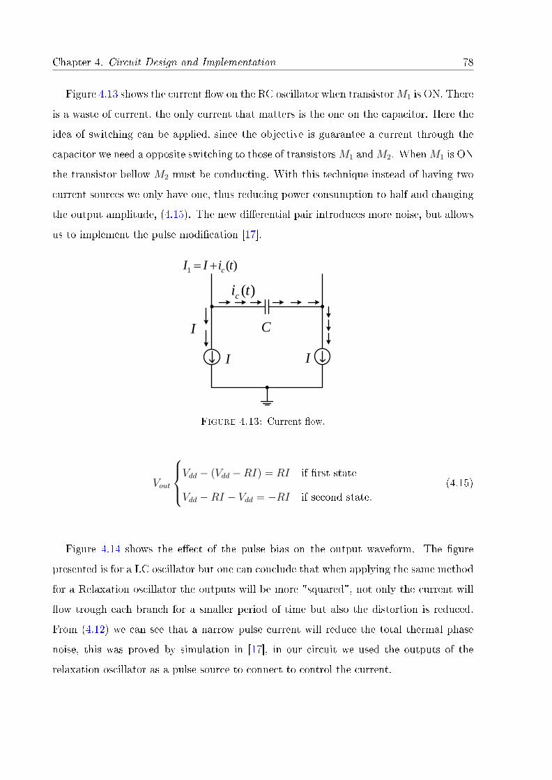
Chapter 4. Circuit Design and Implementation 78
Figure 4.13 shows the current ow on the RC oscillator when transistorM1 is ON. There
is a waste of current, the only current that matters is the one on the capacitor. Here the
idea of switching can be applied, since the objective is guarantee a current through the
capacitor we need a opposite switching to those of transistorsM1 andM2. WhenM1 is ON
the transistor bellow M2 must be conducting. With this technique instead of having two
current sources we only have one, thus reducing power consumption to half and changing
the output amplitude, (4.15). The new dierential pair introduces more noise, but allows
us to implement the pulse modication [17].
I
C
I
)(1 tiII c
)(tic
I
Figure 4.13: Current ow.
Vout
Vdd − (Vdd −RI) = RI if rst state
Vdd −RI − Vdd = −RI if second state.
(4.15)
Figure 4.14 shows the eect of the pulse bias on the output waveform. The gure
presented is for a LC oscillator but one can conclude that when applying the same method
for a Relaxation oscillator the outputs will be more "squared", not only the current will
ow trough each branch for a smaller period of time but also the distortion is reduced.
From (4.12) we can see that a narrow pulse current will reduce the total thermal phase
noise, this was proved by simulation in [17], in our circuit we used the outputs of the
relaxation oscillator as a pulse source to connect to control the current.
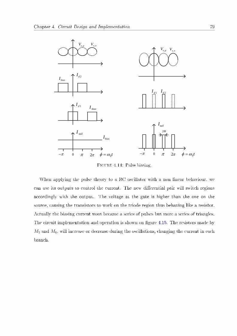
Chapter 4. Circuit Design and Implementation 79
noV ,poV ,
noV ,poV ,
2dI
1dI
tailI
biasI
biasI
biasI
2dI1dI
tailI
0 2 t0 t0 0 2
2
Figure 4.14: Pulse biasing.
When applying the pulse theory to a RC oscillator with a non linear behaviour, we
can use its outputs to control the current. The new dierential pair will switch regions
accordingly with the output. The voltage at the gate is higher than the one on the
source, causing the transistors to work on the triode region thus behaving like a resistor.
Actually the biasing current wont became a series of pulses but more a series of triangles.
The circuit implementation and operation is shown on gure 4.15. The resistors made by
M5 and M6, will increase or decrease during the oscillations, changing the current in each
branch.
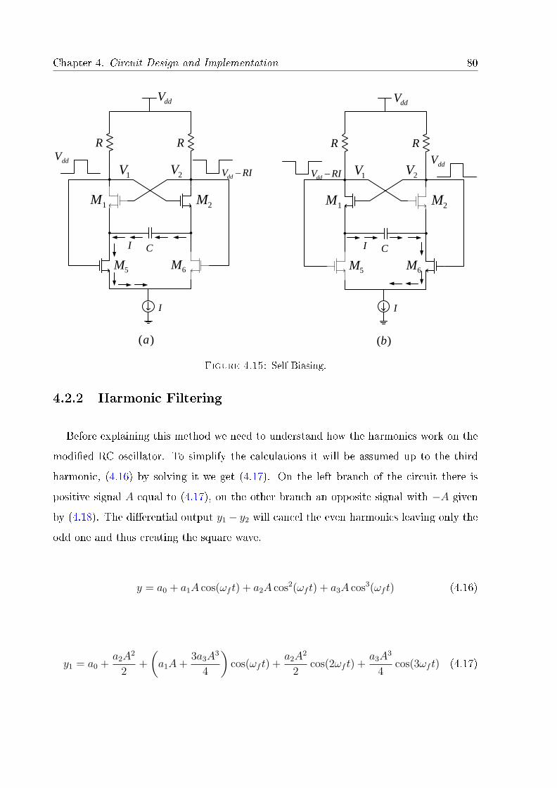
Chapter 4. Circuit Design and Implementation 80
m
C
2M1M
I
5M 6M
2V1V
RR
ddV
RIVdd
I
ddV
m
C
2M1M
I
5M 6M
2V1V
RR
RIVdd
I
ddV
ddV
)(a )(b
Figure 4.15: Self Biasing.
4.2.2 Harmonic Filtering
Before explaining this method we need to understand how the harmonics work on the
modied RC oscillator. To simplify the calculations it will be assumed up to the third
harmonic, (4.16) by solving it we get (4.17). On the left branch of the circuit there is
positive signal A equal to (4.17), on the other branch an opposite signal with −A given
by (4.18). The dierential output y1 − y2 will cancel the even harmonics leaving only the
odd one and thus creating the square wave.
y = a0 + a1A cos(ωf t) + a2A cos2(ωf t) + a3A cos3(ωf t) (4.16)
y1 = a0 +a2A
2
2+
(a1A+
3a3A3
4
)cos(ωf t) +
a2A2
2cos(2ωf t) +
a3A3
4cos(3ωf t) (4.17)
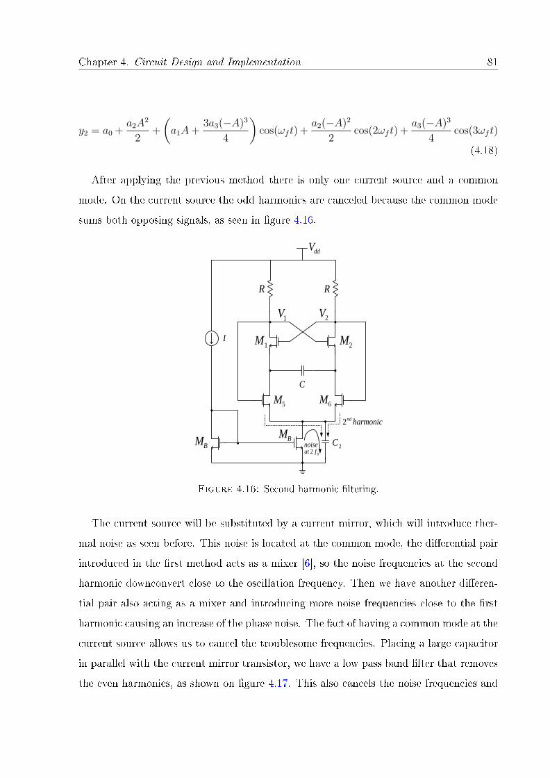
Chapter 4. Circuit Design and Implementation 81
y2 = a0 +a2A
2
2+
(a1A+
3a3(−A)3
4
)cos(ωf t) +
a2(−A)2
2cos(2ωf t) +
a3(−A)3
4cos(3ωf t)
(4.18)
After applying the previous method there is only one current source and a common
mode. On the current source the odd harmonics are canceled because the common mode
sums both opposing signals, as seen in gure 4.16.
C
2M1M
5M 6M
2V1V
RR
ddV
2CBM
BM
I
harmonicnd2
02 fatnoise
Figure 4.16: Second harmonic ltering.
The current source will be substituted by a current mirror, which will introduce ther-
mal noise as seen before. This noise is located at the common mode, the dierential pair
introduced in the rst method acts as a mixer [6], so the noise frequencies at the second
harmonic downconvert close to the oscillation frequency. Then we have another dieren-
tial pair also acting as a mixer and introducing more noise frequencies close to the rst
harmonic causing an increase of the phase noise. The fact of having a common mode at the
current source allows us to cancel the troublesome frequencies. Placing a large capacitor
in parallel with the current mirror transistor, we have a low pass band lter that removes
the even harmonics, as shown on gure 4.17. This also cancels the noise frequencies and
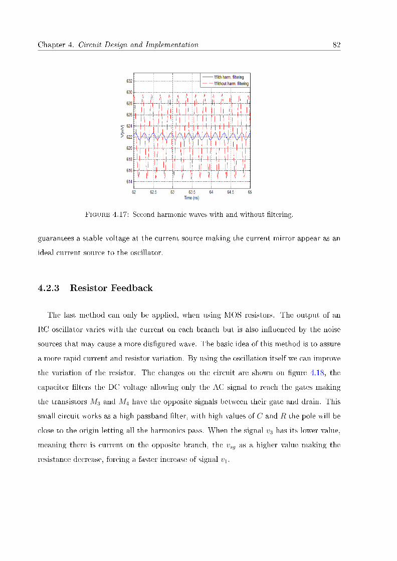
Chapter 4. Circuit Design and Implementation 82
Figure 4.17: Second harmonic waves with and without ltering.
guarantees a stable voltage at the current source making the current mirror appear as an
ideal current source to the oscillator.
4.2.3 Resistor Feedback
The last method can only be applied, when using MOS resistors. The output of an
RC oscillator varies with the current on each branch but is also inuenced by the noise
sources that may cause a more disgured wave. The basic idea of this method is to assure
a more rapid current and resistor variation. By using the oscillation itself we can improve
the variation of the resistor. The changes on the circuit are shown on gure 4.18, the
capacitor lters the DC voltage allowing only the AC signal to reach the gates making
the transistors M3 and M4 have the opposite signals between their gate and drain. This
small circuit works as a high passband lter, with high values of C and R the pole will be
close to the origin letting all the harmonics pass. When the signal v3 has its lower value,
meaning there is current on the opposite branch, the vsg as a higher value making the
resistance decrease, forcing a faster increase of signal v1.
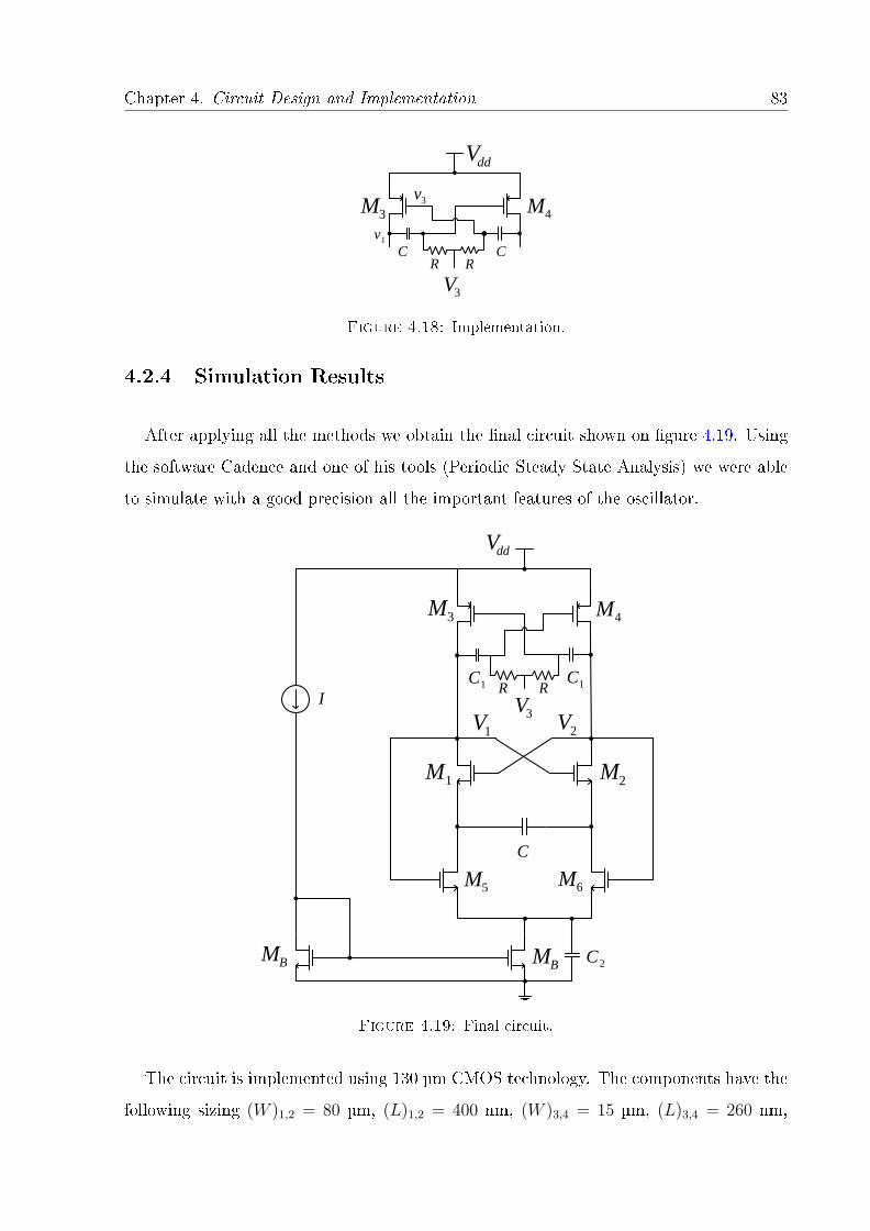
Chapter 4. Circuit Design and Implementation 83
3V
ddV
3M 4M
C CR R
3v
1v
Figure 4.18: Implementation.
4.2.4 Simulation Results
After applying all the methods we obtain the nal circuit shown on gure 4.19. Using
the software Cadence and one of his tools (Periodic Steady State Analysis) we were able
to simulate with a good precision all the important features of the oscillator.
3V
3M4M
1CR R
C
2M1M
I
5M 6M
2V1V
ddV
1C
2CBMBM
Figure 4.19: Final circuit.
The circuit is implemented using 130 µm CMOS technology. The components have the
following sizing (W )1,2 = 80 µm, (L)1,2 = 400 nm, (W )3,4 = 15 µm, (L)3,4 = 260 nm,
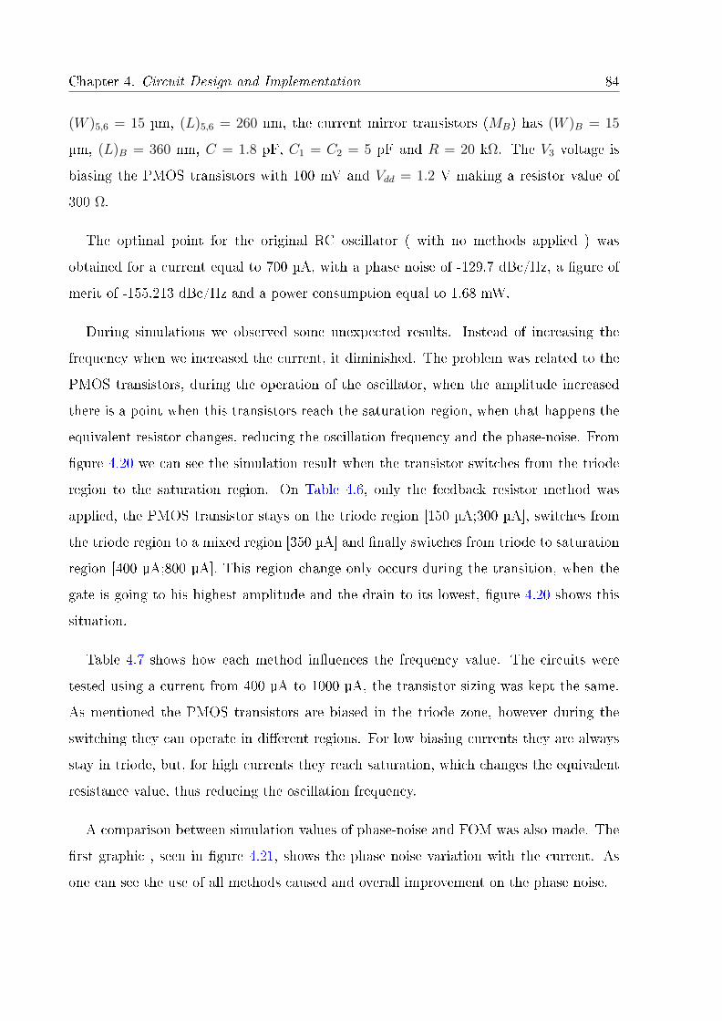
Chapter 4. Circuit Design and Implementation 84
(W )5,6 = 15 µm, (L)5,6 = 260 nm, the current mirror transistors (MB) has (W )B = 15
µm, (L)B = 360 nm, C = 1.8 pF, C1 = C2 = 5 pF and R = 20 kΩ. The V3 voltage is
biasing the PMOS transistors with 100 mV and Vdd = 1.2 V making a resistor value of
300 Ω.
The optimal point for the original RC oscillator ( with no methods applied ) was
obtained for a current equal to 700 µA, with a phase noise of -129.7 dBc/Hz, a gure of
merit of -155.213 dBc/Hz and a power consumption equal to 1.68 mW.
During simulations we observed some unexpected results. Instead of increasing the
frequency when we increased the current, it diminished. The problem was related to the
PMOS transistors, during the operation of the oscillator, when the amplitude increased
there is a point when this transistors reach the saturation region, when that happens the
equivalent resistor changes, reducing the oscillation frequency and the phase-noise. From
gure 4.20 we can see the simulation result when the transistor switches from the triode
region to the saturation region. On Table 4.6, only the feedback resistor method was
applied, the PMOS transistor stays on the triode region [150 µA;300 µA], switches from
the triode region to a mixed region [350 µA] and nally switches from triode to saturation
region [400 µA;800 µA]. This region change only occurs during the transition, when the
gate is going to his highest amplitude and the drain to its lowest, gure 4.20 shows this
situation.
Table 4.7 shows how each method inuences the frequency value. The circuits were
tested using a current from 400 µA to 1000 µA, the transistor sizing was kept the same.
As mentioned the PMOS transistors are biased in the triode zone, however during the
switching they can operate in dierent regions. For low biasing currents they are always
stay in triode, but, for high currents they reach saturation, which changes the equivalent
resistance value, thus reducing the oscillation frequency.
A comparison between simulation values of phase-noise and FOM was also made. The
rst graphic , seen in gure 4.21, shows the phase noise variation with the current. As
one can see the use of all methods caused and overall improvement on the phase noise.
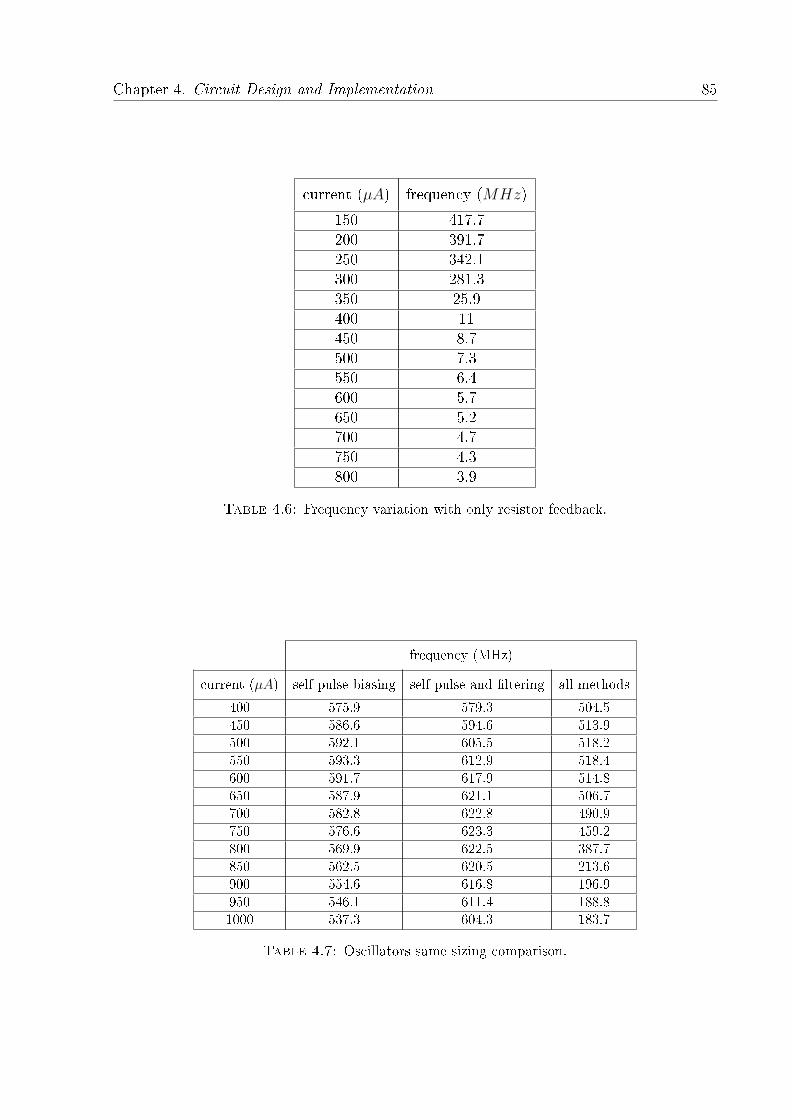
Chapter 4. Circuit Design and Implementation 85
current (µA) frequency (MHz)
150 417.7200 391.7250 342.1300 281.3350 25.9400 11450 8.7500 7.3550 6.4600 5.7650 5.2700 4.7750 4.3800 3.9
Table 4.6: Frequency variation with only resistor feedback.
frequency (MHz)
current (µA) self pulse biasing self pulse and ltering all methods
400 575.9 579.3 504.5450 586.6 594.6 513.9500 592.1 605.5 518.2550 593.3 612.9 518.4600 591.7 617.9 514.8650 587.9 621.1 506.7700 582.8 622.8 490.9750 576.6 623.3 459.2800 569.9 622.5 387.7850 562.5 620.5 213.6900 554.6 616.8 196.9950 546.1 611.4 188.81000 537.3 604.3 183.7
Table 4.7: Oscillators same sizing comparison.
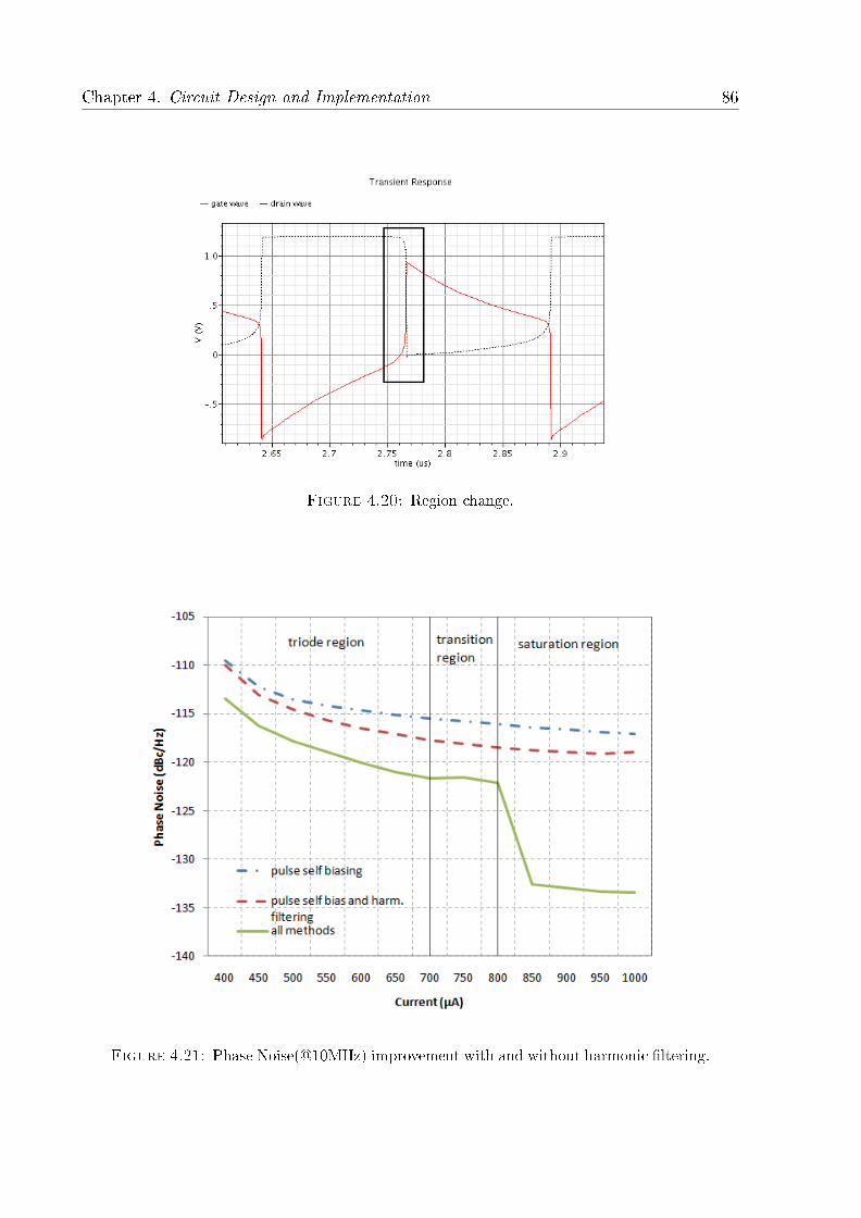
Chapter 4. Circuit Design and Implementation 86
Figure 4.20: Region change.
Figure 4.21: Phase Noise(@10MHz) improvement with and without harmonic ltering.
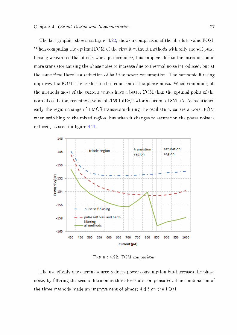
Chapter 4. Circuit Design and Implementation 87
The last graphic, shown on gure 4.22, shows a comparison of the absolute value FOM.
When comparing the optimal FOM of the circuit without methods with only the self pulse
biasing we can see that it as a worst performance, this happens due to the introduction of
more transistor causing the phase noise to increase due to thermal noise introduced, but at
the same time there is a reduction of half the power consumption. The harmonic ltering
improves the FOM, this is due to the reduction of the phase noise. When combining all
the methods most of the current values have a better FOM than the optimal point of the
normal oscillator, reaching a value of -159.1 dBc/Hz for a current of 850 µA. As mentioned
early the region change of PMOS transistors during the oscillation, causes a worst FOM
when switching to the mixed region, but when it changes to saturation the phase noise is
reduced, as seen on gure 4.21.
Figure 4.22: FOM comparison.
The use of only one current source reduces power consumption but increases the phase
noise, by ltering the second harmonics those loses are compensated. The combination of
the three methods made an improvement of almost 4 dB on the FOM.
Chapter 4. Circuit Design and Implementation 88
An attempt to obtain quadrature outputs was made by connecting transistors M5 and
M6 to the output of the other oscillator. The results obtained were unsatisfactory, the
frequency would always drop when we increased the current,thus reducing the FOM. We
also tried coupling through the second harmonic using the current sources ([23]), the
results were similar to the ones we saw for a single oscillator with a improvement of 1 to
2 dB on the FOM.
4.3 Fully Integrated CMOS Two-Integrator
We have seen the circuit implementation of the two integrator in a previous chapter,
before we go into the simulation results we need to make some modications. We did
not use capacitors for oscillation, the parasitic capacitors in the transistors were enough.
Based on the harmonic ltering mentioned on the previous section, we decided to use
a capacitor connected between both common modes to cancel the even harmonics. The
resistors were substituted by PMOS transistors in the triode region also the capacitor is
substituted by transistors.
4.3.1 CMOS Capacitors
CMOS transistor have a capacitance between the gate and the substrate Cox. Depend-
ing on the gate voltage we consider three dierent bias modes. One below the at-band
voltage, VFB, a second between the at-band voltage and the threshold voltage, Vth, and
nally one larger than the threshold voltage, [21]. These bias regimes are called the
accumulation, depletion and inversion mode of operation, as shown on gure 4.23.
In accumulation mode the negative charge on the gate attracts holes from the substrate
to the oxide-semiconductor interface. Only a small amount of band bending is needed to
build up the accumulation charge so that almost all of the potential variation is within
the oxide. The capacitance is equal to Cox.
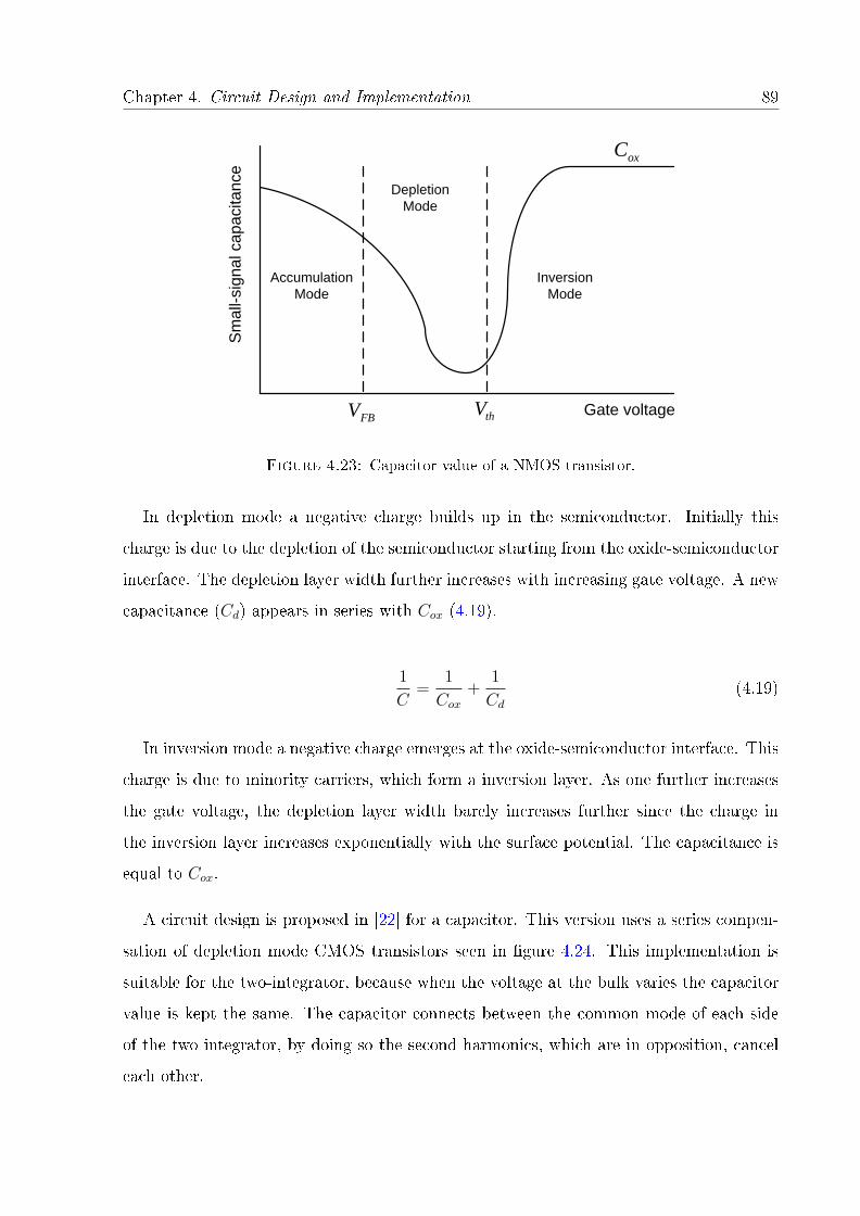
Chapter 4. Circuit Design and Implementation 89
FBV thV Gate voltage
oxC
Sm
all-
sig
na
l ca
pa
cita
nce
Accumulation
Mode
Depletion
Mode
Inversion
Mode
Figure 4.23: Capacitor value of a NMOS transistor.
In depletion mode a negative charge builds up in the semiconductor. Initially this
charge is due to the depletion of the semiconductor starting from the oxide-semiconductor
interface. The depletion layer width further increases with increasing gate voltage. A new
capacitance (Cd) appears in series with Cox (4.19).
1
C=
1
Cox+
1
Cd(4.19)
In inversion mode a negative charge emerges at the oxide-semiconductor interface. This
charge is due to minority carriers, which form a inversion layer. As one further increases
the gate voltage, the depletion layer width barely increases further since the charge in
the inversion layer increases exponentially with the surface potential. The capacitance is
equal to Cox.
A circuit design is proposed in [22] for a capacitor. This version uses a series compen-
sation of depletion mode CMOS transistors seen in gure 4.24. This implementation is
suitable for the two-integrator, because when the voltage at the bulk varies the capacitor
value is kept the same. The capacitor connects between the common mode of each side
of the two integrator, by doing so the second harmonics, which are in opposition, cancel
each other.
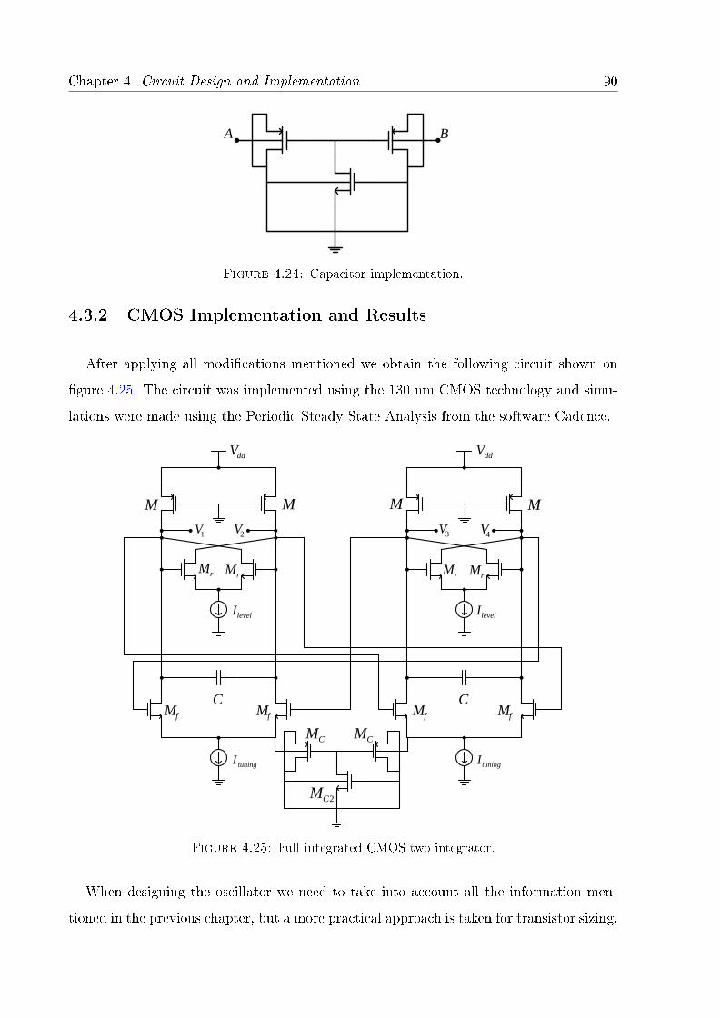
Chapter 4. Circuit Design and Implementation 90
A B
Figure 4.24: Capacitor implementation.
4.3.2 CMOS Implementation and Results
After applying all modications mentioned we obtain the following circuit shown on
gure 4.25. The circuit was implemented using the 130 nm CMOS technology and simu-
lations were made using the Periodic Steady State Analysis from the software Cadence.
rM
fM
levelI levelI
tuningI tuningI
ddV ddV
C C
1V 2V 3V4V
rM rMrM
fM fM fM
MM M M
CM CM
2CM
Figure 4.25: Full integrated CMOS two integrator.
When designing the oscillator we need to take into account all the information men-
tioned in the previous chapter, but a more practical approach is taken for transistor sizing.
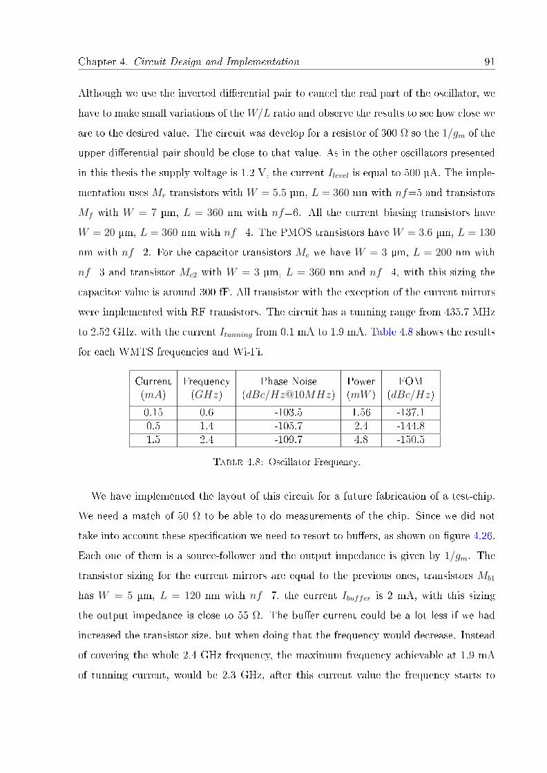
Chapter 4. Circuit Design and Implementation 91
Although we use the inverted dierential pair to cancel the real part of the oscillator, we
have to make small variations of theW/L ratio and observe the results to see how close we
are to the desired value. The circuit was develop for a resistor of 300 Ω so the 1/gm of the
upper dierential pair should be close to that value. As in the other oscillators presented
in this thesis the supply voltage is 1.2 V, the current Ilevel is equal to 500 µA. The imple-
mentation uses Mr transistors with W = 5.5 µm, L = 360 nm with nf=5 and transistors
Mf with W = 7 µm, L = 360 nm with nf=6. All the current biasing transistors have
W = 20 µm, L = 360 nm with nf=4. The PMOS transistors have W = 3.6 µm, L = 130
nm with nf=2. For the capacitor transistors Mc we have W = 3 µm, L = 200 nm with
nf=3 and transistor Mc2 with W = 3 µm, L = 360 nm and nf=4, with this sizing the
capacitor value is around 300 fF. All transistor with the exception of the current mirrors
were implemented with RF transistors. The circuit has a tunning range from 435.7 MHz
to 2.52 GHz, with the current Itunning from 0.1 mA to 1.9 mA. Table 4.8 shows the results
for each WMTS frequencies and Wi-Fi.
Current Frequency Phase Noise Power FOM(mA) (GHz) (dBc/Hz@10MHz) (mW ) (dBc/Hz)
0.15 0.6 -103.5 1.56 -137.10.5 1.4 -105.7 2.4 -144.81.5 2.4 -109.7 4.8 -150.5
Table 4.8: Oscillator Frequency.
We have implemented the layout of this circuit for a future fabrication of a test-chip.
We need a match of 50 Ω to be able to do measurements of the chip. Since we did not
take into account these specication we need to resort to buers, as shown on gure 4.26.
Each one of them is a source-follower and the output impedance is given by 1/gm. The
transistor sizing for the current mirrors are equal to the previous ones, transistors Mb1
has W = 5 µm, L = 120 nm with nf=7, the current Ibuffer is 2 mA, with this sizing
the output impedance is close to 55 Ω. The buer current could be a lot less if we had
increased the transistor size, but when doing that the frequency would decrease. Instead
of covering the whole 2.4 GHz frequency, the maximum frequency achievable at 1.9 mA
of tunning current, would be 2.3 GHz, after this current value the frequency starts to
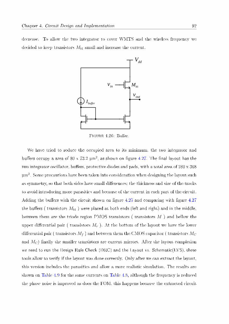
Chapter 4. Circuit Design and Implementation 92
decrease. To allow the two integrator to cover WMTS and the wireless frequency we
decided to keep transistors Mb1 small and increase the current.
ddV
bufferI
inv
outv
1bM
Figure 4.26: Buer.
We have tried to reduce the occupied area to its minimum, the two integrator and
buers occupy a area of 80 x 73.2 µm2, as shown on gure 4.27. The nal layout has the
two integrator oscillator, buers, protective diodes and pads, with a total area of 280 x 368
µm2. Some precautions have been taken into consideration when designing the layout such
as symmetry, so that both sides have small dierences; the thickness and size of the tracks
to avoid introducing more parasitics and because of the current in each part of the circuit.
Adding the buers with the circuit shown on gure 4.25 and comparing with gure 4.27
the buers ( transistorsMb1 ) were placed at both ends (left and right) and in the middle,
between them are the triode region PMOS transistors ( transistors M ) and bellow the
upper dierential pair ( transistors Mr ). At the bottom of the layout we have the lower
dierential pair ( transistorsMf ) and between them the CMOS capacitor ( transistorsMC
and MC) nally the smaller transistors are current mirrors. After the layout completion
we need to run the Design Rule Check (DRC) and the Layout vs. Schematic(LVS), these
tools allow to verify if the layout was done correctly. Only after we can extract the layout,
this version includes the parasitics and allow a more realistic simulation. The results are
shown on Table 4.9 for the same currents on Table 4.8, although the frequency is reduced
the phase noise is improved as does the FOM, this happens because the extracted circuit
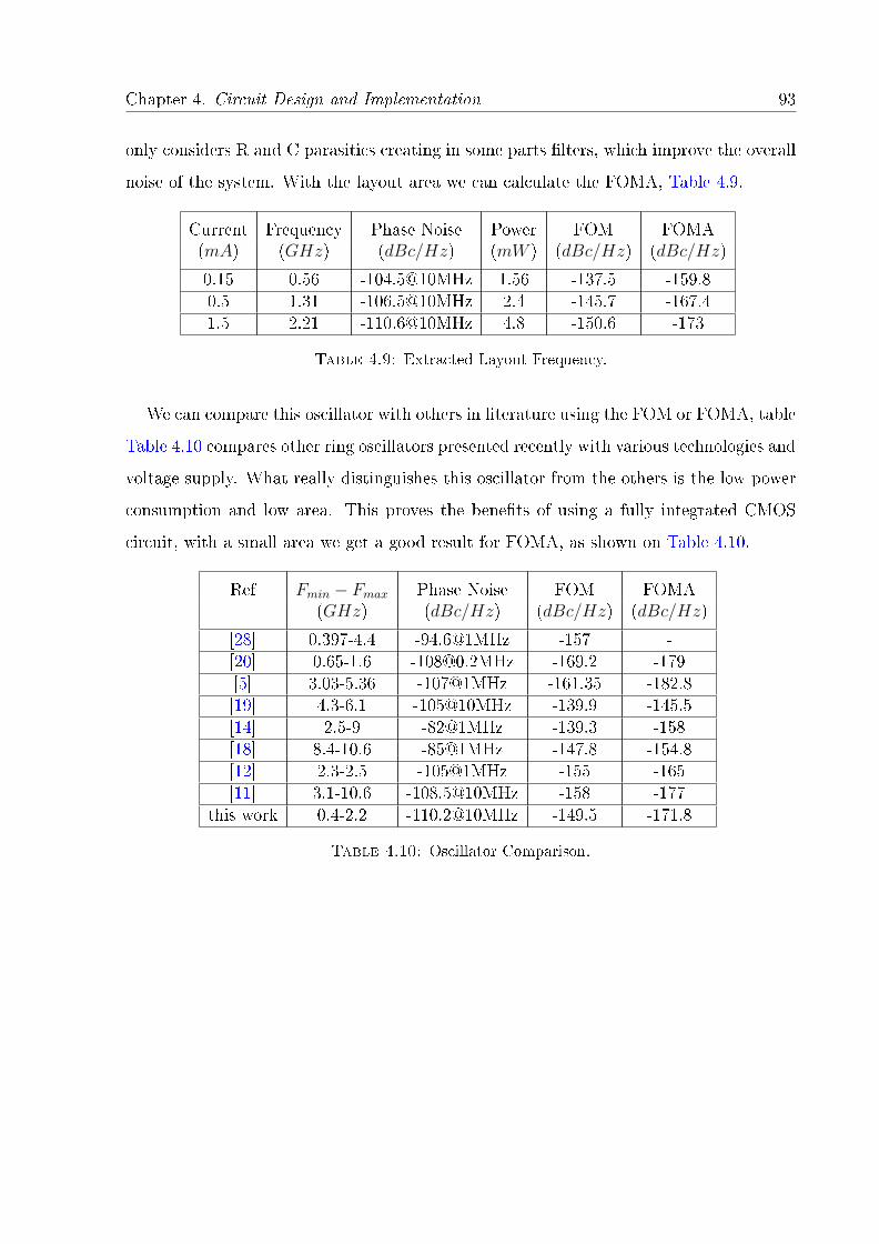
Chapter 4. Circuit Design and Implementation 93
only considers R and C parasitics creating in some parts lters, which improve the overall
noise of the system. With the layout area we can calculate the FOMA, Table 4.9.
Current Frequency Phase Noise Power FOM FOMA(mA) (GHz) (dBc/Hz) (mW ) (dBc/Hz) (dBc/Hz)
0.15 0.56 -104.5@10MHz 1.56 -137.5 -159.80.5 1.31 -106.5@10MHz 2.4 -145.7 -167.41.5 2.21 -110.6@10MHz 4.8 -150.6 -173
Table 4.9: Extracted Layout Frequency.
We can compare this oscillator with others in literature using the FOM or FOMA, table
Table 4.10 compares other ring oscillators presented recently with various technologies and
voltage supply. What really distinguishes this oscillator from the others is the low power
consumption and low area. This proves the benets of using a fully integrated CMOS
circuit, with a small area we get a good result for FOMA, as shown on Table 4.10.
Ref Fmin − Fmax Phase Noise FOM FOMA(GHz) (dBc/Hz) (dBc/Hz) (dBc/Hz)
[28] 0.397-4.4 -94.6@1MHz -157 -[20] 0.65-1.6 [email protected] -169.2 -179[5] 3.03-5.36 -107@1MHz -161.35 -182.8[19] 4.3-6.1 -105@10MHz -139.9 -145.5[14] 2.5-9 -82@1MHz -139.3 -158[18] 8.4-10.6 -85@1MHz -147.8 -154.8[12] 2.3-2.5 -105@1MHz -155 -165[11] 3.1-10.6 -108.5@10MHz -158 -177
this work 0.4-2.2 -110.2@10MHz -149.5 -171.8
Table 4.10: Oscillator Comparison.
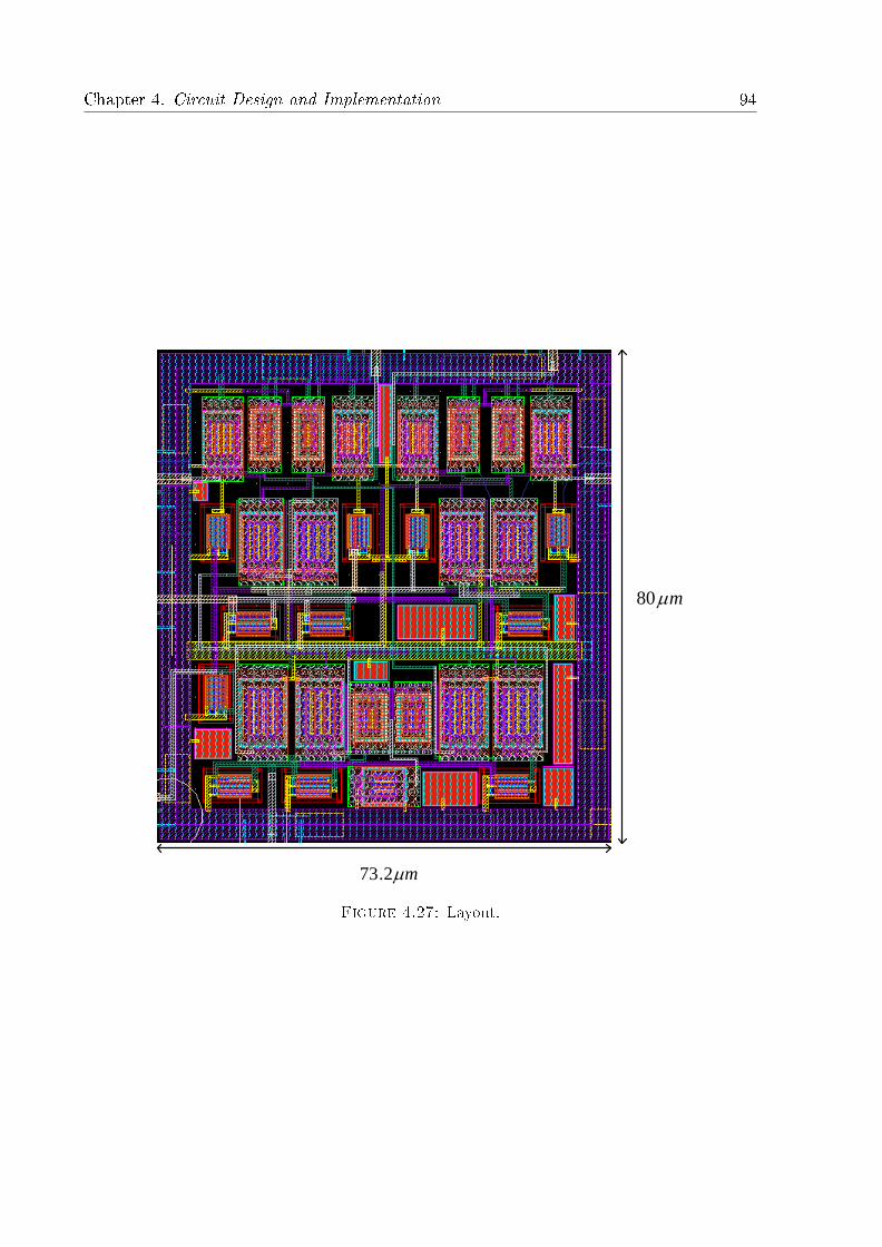
Chapter 4. Circuit Design and Implementation 94
m80
m2.73
Figure 4.27: Layout.
Chapter 5
Conclusions and Future Work
In this thesis we have implemented various oscillators with the objective to comply
to the demands of low area, low power consumption, and accurate quadrature outputs.
Coupled RC oscillators prove to be a good solution, although single LC oscillator have a
better phase noise, they occupy a larger area and when used in quadrature their advantage
is lost.
The rst circuit presented shows not only a noise improvement in a coupled RC os-
cillator, but also, how the circuit reacts with mismatches and how much time it takes
to synchronize. RC oscillators allow to build a fully integrated CMOS circuit, with this
feature we can develop methods to reduce the overall noise. For this purpose, three meth-
ods were presented one of them being completely new. With all methods applied to a
simple Relaxation oscillator we obtained a phase noise improvement of almost 5 dB. The
last circuit was a fully integrated CMOS two integrator with a small area, reduced power
consumption, and wide tunning range, its performance were compared with other ring
oscillators proposed in recent years.
The CMOS current controlled quadrature oscillator was able to operate in the frequency
range of WMTS applications. We tested two types of coupling "hard" and "soft", with
the rst one showing better results in phase noise, about 2 dB for 600 MHz and 4 dB for
1.4 GHz and also concerning mismatches. The circuit was submitted to a external current
with a frequency that is an odd multiple of the oscillation frequency, the oscillator was
95
Chapter 5. Conclusions and Future Work 96
able to synchronize after a few periods. At higher frequencies for the "soft" coupling the
oscillations stopped, we were unable to determine the reason, further investigation can be
made in this matter.
Three methods to reduce phase noise and improve the FOM were implemented. These
methods were tested separately and compared with the optimum point before the appli-
cation of the methods. The new technique introduced in this thesis improves the overall
noise, but causes the PMOS transistors to leave the linear region and enter the satura-
tion, during transitions. This situation caused a great reduction of the phase noise around
( -132.6 dBc/Hz@10 MHz ) but also decreased the frequency around 300 MHz with all
methods applied, making a FOM of -159.1 dBc/Hz. The other methods aected the power
consumption and the current thermal noise. The pulse self biasing method could have
better results by controlling the width of the pulses.
The two integrator covered the WMTS and wireless frequencies. All the resistors and
capacitors were implemented with CMOS transistors, making the layout area small, with
a total area of 5.856x10⁻³ mm2 without pads. The fully integrated CMOS circuit shows
that it is possible to reduce the occupied area by simply using transistors, there are some
implementations that combine this oscillator with a mixer, reducing the total area of a
transceiver.
5.1 Future Work
− Layout implementation for all circuits, for future fabrication and measurements;
− The techniques showed can be further applied to other oscillators at higher frequen-
cies;
− New methods can be developed with the substitution of passive elements by tran-
sistors.
− Combine more receiver blocks such as the LNA in a single chip, using CMOS tech-
nology.

Appendix A
Submitted Papers
97

A.1 JMCS, 2010
Analysis and Design of CMOS Coupled Multivibrators
International Journal of Microelectronics and Computer Science

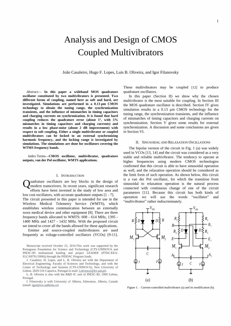
1
Abstract— In this paper a wideband MOS quadrature
oscillator constituted by two multivibrators is presented. Two
different forms of coupling, named here as soft and hard, are
investigated. Simulations are performed in a 0.13 µm CMOS
technology to obtain the tuning range, the synchronization
transients, and the influence of mismatches in timing capacitors
and charging currents on synchronization. It is found that hard
coupling reduces the quadrature error (about 1º, with 5%
mismatches in timing capacitors and charging currents) and
results in a low phase-noise (about 2 dB improvement) with
respect to soft coupling. Either a single multivibrator or coupled
multivibrators can be locked to an external synchronizing
harmonic frequency, and the locking range is investigated by
simulations. The simulations are done for oscillators covering the
WTMS frequency bands.
Index Terms—CMOS oscillator, multivibrator, quadrature
outputs, van der Pol oscillator, WMTS applications.
I. INTRODUCTION
uadrature oscillators are key blocks in the design of
modern transceivers. In recent years, significant research
efforts have been invested in the study of low area and
low cost oscillators, with accurate quadrature outputs [1 - 7].
The circuit presented in this paper is intended for use in the
Wireless Medical Telemetry Service (WMTS), which
establishes wireless communication between an externally
worn medical device and other equipment [8]. There are three
frequency bands allocated to WMTS: 608 - 614 MHz, 1395 -
1400 MHz and 1427 - 1432 MHz. With the proposed circuit
we intend to cover all the bands allowed for these applications.
Emitter and source-coupled multivibrators are used
frequently as voltage-controlled oscillators (VCOs) [9-11].
Manuscript received October 25, 2010.This work was supported by the
Portuguese Foundation for Science and Technology (CTS-UNINOVA and
INESC-ID multiannual funding and project LEADER (PTDC/EEA-
ELC/69791/2006)) through the PIDDAC Program funds.
J. Casaleiro, H. Lopes, and L. B. Oliveira are with the Department of
Electrical Engineering, Faculty of Sciences and Technology, and with the
Center of Technology and Systems (CTS-UNINOVA), New University of
Lisbon, 2829-516 Caparica, Portugal (e-mail: [email protected]).
L. B. Oliveira is also with the R&D IC unit of INESC-ID, 1000 Lisbon,
Portugal. I. Filanovsky is with University of Alberta, Edmonton, Alberta, Canada
(email: [email protected])
These multivibrators may be coupled [12] to produce
quadrature oscillators.
In this paper (Section II) we show why the chosen
multivibrator is the most suitable for coupling. In Section III
the MOS quadrature oscillator is described. Section IV gives
simulation results in a 0.13 µm CMOS technology for the
tuning range, the synchronization transients, and the influence
of mismatches of timing capacitors and charging currents on
synchronization. Section V gives some results for external
synchronization. A discussion and some conclusions are given
in Section VI.
II. SINUSOIDAL AND RELAXATION OSCILLATIONS
The bipolar version of the circuit in Fig. 1 (a) was widely
used in VCOs [13, 14] and the circuit was considered as a very
stable and reliable multivibrator. The tendency to operate at
higher frequencies using modern CMOS technologies
confirmed that this circuit is able to have sinusoidal operation
as well, and the relaxation operation should be considered as
the limit form of such operation. As shown below, this circuit
is a van der Pol oscillator, for which the transition from
sinusoidal to relaxation operation is the natural process
connected with continuous change of one of the circuit
parameters [11]. Because this circuit has both kinds of
operation we will use the words “oscillator” and
“multivibrator” rather indiscriminately.
I
DDV
C
RR
I
D D
ICI
D D2R
1R
DDV
)(a )(b
B 1B
1E
1A
E
A
2R
1R
1M 2M
1M 2M
Figure 1. Current-controlled multivibrator (a) and its modification (b).
Analysis and Design of CMOS
Coupled Multivibrators
João Casaleiro, Hugo F. Lopes, Luis B. Oliveira, and Igor Filanovsky
Q
2
Assume that the oscillation amplitude developed on
resistors R is so small that the diodes are OFF. Using
simplified models (controlled transconductance and gate-
source capacitance) for transistors M1 and M2 it is possible to
show that the capacitor C “sees” the impedance
1 2
1 2
( ) ( ) 2gs m min
m m
C s G g gz
G g g G
(1)
where 1/G R . The oscillator characteristic equation is
(1/ ) 0inCs z (2)
Substituting (1) in (2) one obtains that
2 1 2 1 2
1 2 1 2
11 2 0
( )
m m m m
gs m m gs m m
g g g gs R s
RC g g RCC g g
(3)
When the oscillation starts one may consider that
1 2 0 2 ( / )m m m n oxg g g C W L I , and (3) can be rewritten
as
2 00
11 0
2
mm
gs gs
gs Rg s
RC RCC (4)
The oscillations will start if the roots of this equation are
located in the right half of the s-plane. This requires that
0 1/mg R (5)
The oscillations will have the frequency
0 0 /(2 )m gsg RCC (6)
The roots of (4) are
2
0 0 01,2
1 1
2 2 2
m m m
gs gs gs
g R g R gs
RC RC RCC
(7)
If C varies and all other parameters are constant, the roots
move in the right half of the s-plane only. For small values of
C they are complex-conjugate and located in the vicinity of
jω-axis. The oscillator has quasi-sinusoidal oscillations). With
increase of C they move towards the positive real axis. The
oscillations become more and more distorted. When 2
0 0(2 ) /( 1)gs m mC C g R g R ) the roots are positive real axis,
and one may consider that the circuit has now relaxation
oscillations. With further increase of C the roots move along
positive real axis arriving to the final values of 1 0s and
2 0( 1) /( )m gss Rg rC . The circuit oscillations are closer and
closer to relaxation oscillations with discontinuous waveform.
The transition from sinusoidal to relaxation oscillations is
smooth with a gradual increase of distortions in the waveform
[10] and specific amplitude limiting.
Let us do the approximation
2
1 2 0
1 2
12 2
m m m
m m
g g g i
g g I
(8)
in the damping term of (3), and leave the frequency term the
same as in (4). Here i is the capacitor current. Then, one can
write for this current the differential equation
222
0 02
11 1 0
2m
gs
d i i diRg i
dt RC dtI
(9)
Introducing the normalized variable /( 2 )x i I and using the
notation 0 0( 1) /(2 )m gsRg RC and 2 0 /(2 )m gsg C , one
reduces this equation to the standard van der Pol form
22 2
0 2 022( ) 0
d x dxx x
dt dt (10)
The solution of this equation for small distortions is
0 2 0 0 02 / sin 2 1 (1/ ) sinmx t Rg t (11)
The amplitude of the voltage between the drain resistors (the
usual points of measurements) will be
04 2 1 (1/ )dm mV I Rg (11)
If this amplitudes increases (say, if I increases as a result of
tuning) the diodes eventually limit the amplitude. When the
circuit moves to relaxation oscillation (at lower frequency)
then the amplitude limiting by the diodes is dominating. The
frequency may be approximated as
0 ( )/(4 )BE ONf I V C (12)
where ( ) 0.5BE ONV V (MOS diodes) is the voltage drop on the
diode-connected transistors D.
Due to the smooth transition from sinusoidal to relaxation
oscillations and the existence of amplitude stabilization
mechanisms, the frequency tuning range may be very wide
[13 - 15]. It can be further increased by the modification
shown in Fig. 1 b that allows higher oscillation frequencies,
and is suitable for coupling two multivibrators in a quadrature
oscillator. The voltage amplitude at the timing capacitor is
now lower, but the oscillation frequency is
0 ( ) 1 1 2/4 /[( ) ]BE ONf I V R R R C (13)
To obtain a quadrature oscillator one couples two similar
oscillators using differential pairs [12, 16]. The inputs of the
coupling differential pairs should be connected to the timing
capacitors (at A and A1). Their outputs can be connected either
to nodes B and B1 or E and E1. A source with incremental
current Ic injected at node B will create an incremental voltage
Vb
1 2 1 2( ) /( )b cV I R R R R (14)
(assuming that 2Rrd , where dr is the diode dynamic
resistance). If Ic is injected at node E then Vb will be reduced
to
1 1 2( ) /( )b c dV I R r R R (15)
assuming that 1 2dr R R .
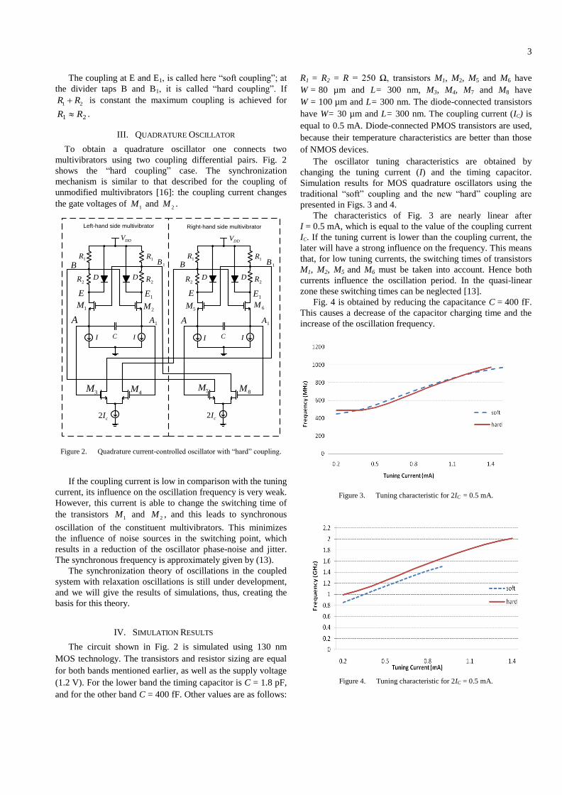
3
The coupling at E and E1, is called here “soft coupling”; at
the divider taps B and B1, it is called “hard coupling”. If
1 2R R is constant the maximum coupling is achieved for
21 RR .
III. QUADRATURE OSCILLATOR
To obtain a quadrature oscillator one connects two
multivibrators using two coupling differential pairs. Fig. 2
shows the “hard coupling” case. The synchronization
mechanism is similar to that described for the coupling of
unmodified multivibrators [16]: the coupling current changes
the gate voltages of 1M and
2M .
ICI
D D
1M2M
2R
1R
DDV
B 1B
1E
1A
E
A
2R
1R
ICI
D D
5M 6M
2R
1R
DDV
B 1B
1E
1A
E
A
2R
1R
cI2
8M7M
Left-hand side multivibrator Right-hand side multivibrator
cI2
3M4M
Figure 2. Quadrature current-controlled oscillator with “hard” coupling.
If the coupling current is low in comparison with the tuning
current, its influence on the oscillation frequency is very weak.
However, this current is able to change the switching time of
the transistors 1M and 2M , and this leads to synchronous
oscillation of the constituent multivibrators. This minimizes
the influence of noise sources in the switching point, which
results in a reduction of the oscillator phase-noise and jitter.
The synchronous frequency is approximately given by (13).
The synchronization theory of oscillations in the coupled
system with relaxation oscillations is still under development,
and we will give the results of simulations, thus, creating the
basis for this theory.
IV. SIMULATION RESULTS
The circuit shown in Fig. 2 is simulated using 130 nm
MOS technology. The transistors and resistor sizing are equal
for both bands mentioned earlier, as well as the supply voltage
(1.2 V). For the lower band the timing capacitor is C = 1.8 pF,
and for the other band C = 400 fF. Other values are as follows:
R1 = R2 = R = 250 Ω, transistors M1, M2, M5 and M6 have
W = 80 µm and L= 300 nm, M3, M4, M7 and M8 have
W = 100 µm and L= 300 nm. The diode-connected transistors
have W= 30 µm and L= 300 nm. The coupling current (IC) is
equal to 0.5 mA. Diode-connected PMOS transistors are used,
because their temperature characteristics are better than those
of NMOS devices.
The oscillator tuning characteristics are obtained by
changing the tuning current (I) and the timing capacitor.
Simulation results for MOS quadrature oscillators using the
traditional “soft” coupling and the new “hard” coupling are
presented in Figs. 3 and 4.
The characteristics of Fig. 3 are nearly linear after
I = 0.5 mA, which is equal to the value of the coupling current
IC. If the tuning current is lower than the coupling current, the
later will have a strong influence on the frequency. This means
that, for low tuning currents, the switching times of transistors
M1, M2, M5 and M6 must be taken into account. Hence both
currents influence the oscillation period. In the quasi-linear
zone these switching times can be neglected [13].
Fig. 4 is obtained by reducing the capacitance C = 400 fF.
This causes a decrease of the capacitor charging time and the
increase of the oscillation frequency.
Figure 3. Tuning characteristic for 2IC = 0.5 mA.
Figure 4. Tuning characteristic for 2IC = 0.5 mA.
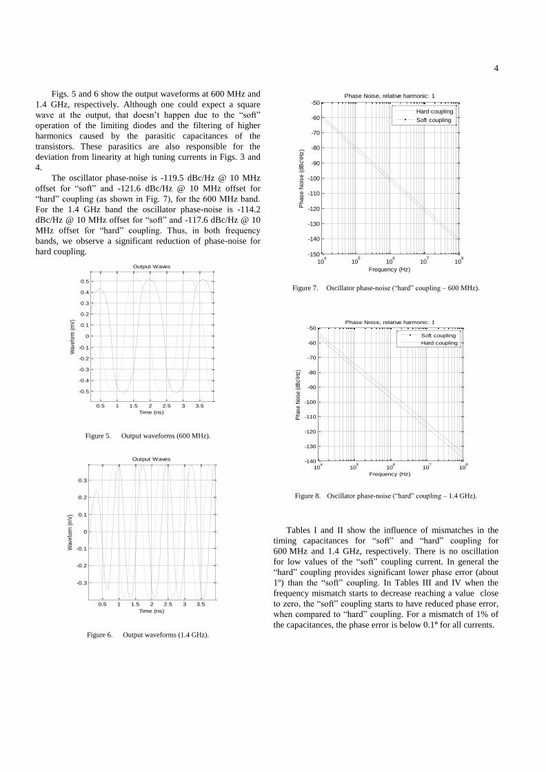
4
Figs. 5 and 6 show the output waveforms at 600 MHz and
1.4 GHz, respectively. Although one could expect a square
wave at the output, that doesn’t happen due to the “soft”
operation of the limiting diodes and the filtering of higher
harmonics caused by the parasitic capacitances of the
transistors. These parasitics are also responsible for the
deviation from linearity at high tuning currents in Figs. 3 and
4.
The oscillator phase-noise is -119.5 dBc/Hz @ 10 MHz
offset for “soft” and -121.6 dBc/Hz @ 10 MHz offset for
“hard” coupling (as shown in Fig. 7), for the 600 MHz band.
For the 1.4 GHz band the oscillator phase-noise is -114.2
dBc/Hz @ 10 MHz offset for “soft” and -117.6 dBc/Hz @ 10
MHz offset for “hard” coupling. Thus, in both frequency
bands, we observe a significant reduction of phase-noise for
hard coupling.
0.5 1 1.5 2 2.5 3 3.5
-0.5
-0.4
-0.3
-0.2
-0.1
0
0.1
0.2
0.3
0.4
0.5
Time (ns)
Wav
efor
m (
mV
)
Output Waves
Figure 5. Output waveforms (600 MHz).
0.5 1 1.5 2 2.5 3 3.5
-0.3
-0.2
-0.1
0
0.1
0.2
0.3
Time (ns)
Wav
efor
m (
mV
)
Output Waves
Figure 6. Output waveforms (1.4 GHz).
104
105
106
107
108
-150
-140
-130
-120
-110
-100
-90
-80
-70
-60
-50
Frequency (Hz)
Phase N
ois
e (
dB
c\H
z)
Phase Noise, relative harmonic: 1
Hard coupling
Soft coupling
Figure 7. Oscillator phase-noise (“hard” coupling – 600 MHz).
104
105
106
107
108
-140
-130
-120
-110
-100
-90
-80
-70
-60
-50
Frequency (Hz)
Pha
se N
oise
(dB
c\H
z)
Phase Noise, relative harmonic: 1
Soft coupling
Hard coupling
Figure 8. Oscillator phase-noise (“hard” coupling – 1.4 GHz).
Tables I and II show the influence of mismatches in the
timing capacitances for “soft” and “hard” coupling for
600 MHz and 1.4 GHz, respectively. There is no oscillation
for low values of the “soft” coupling current. In general the
“hard” coupling provides significant lower phase error (about
1º) than the “soft” coupling. In Tables III and IV when the
frequency mismatch starts to decrease reaching a value close
to zero, the “soft” coupling starts to have reduced phase error,
when compared to “hard” coupling. For a mismatch of 1% of
the capacitances, the phase error is below 0.1º for all currents.
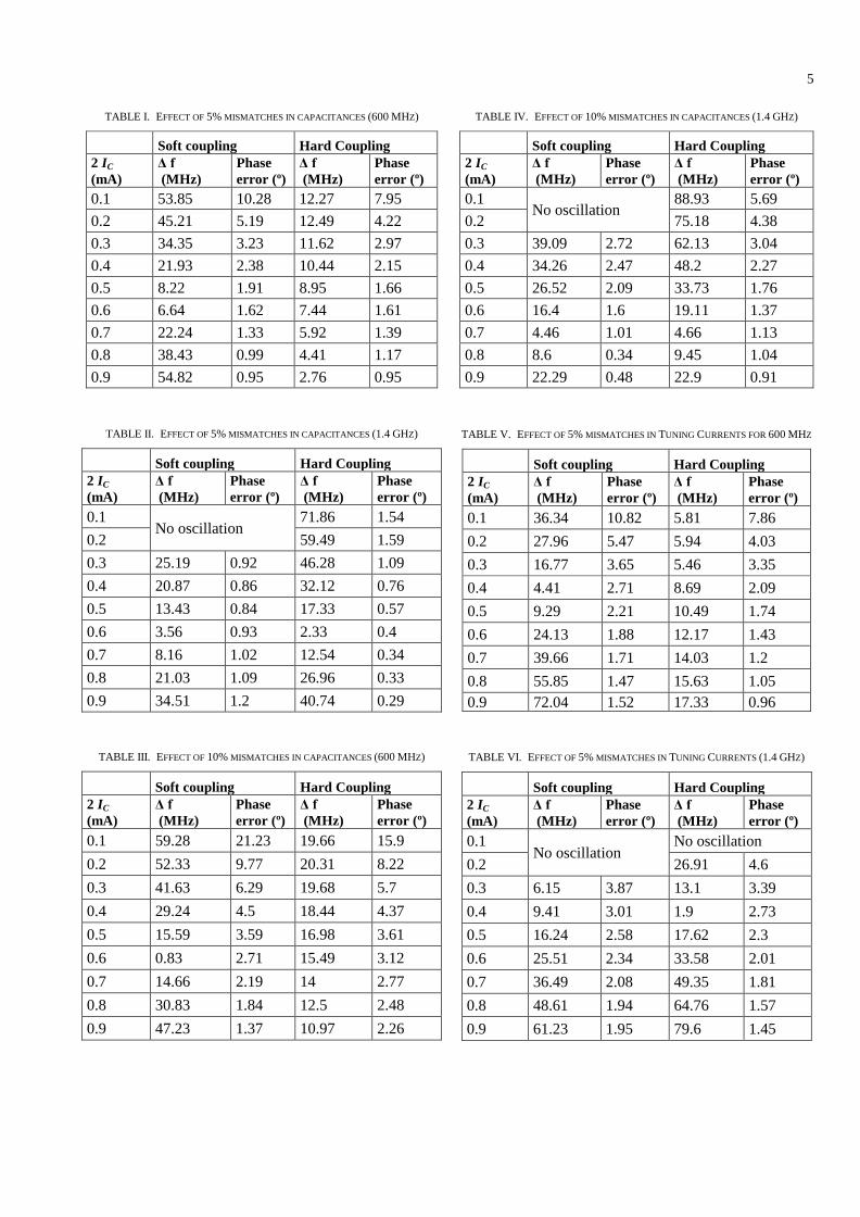
5
TABLE I. EFFECT OF 5% MISMATCHES IN CAPACITANCES (600 MHZ)
Soft coupling Hard Coupling
2 IC
(mA)
Δ f
(MHz)
Phase
error (º)
Δ f
(MHz)
Phase
error (º)
0.1 53.85 10.28 12.27 7.95
0.2 45.21 5.19 12.49 4.22
0.3 34.35 3.23 11.62 2.97
0.4 21.93 2.38 10.44 2.15
0.5 8.22 1.91 8.95 1.66
0.6 6.64 1.62 7.44 1.61
0.7 22.24 1.33 5.92 1.39
0.8 38.43 0.99 4.41 1.17
0.9 54.82 0.95 2.76 0.95
TABLE II. EFFECT OF 5% MISMATCHES IN CAPACITANCES (1.4 GHZ)
Soft coupling Hard Coupling
2 IC
(mA)
Δ f
(MHz)
Phase
error (º)
Δ f
(MHz)
Phase
error (º)
0.1 No oscillation
71.86 1.54
0.2 59.49 1.59
0.3 25.19 0.92 46.28 1.09
0.4 20.87 0.86 32.12 0.76
0.5 13.43 0.84 17.33 0.57
0.6 3.56 0.93 2.33 0.4
0.7 8.16 1.02 12.54 0.34
0.8 21.03 1.09 26.96 0.33
0.9 34.51 1.2 40.74 0.29
TABLE III. EFFECT OF 10% MISMATCHES IN CAPACITANCES (600 MHZ)
Soft coupling Hard Coupling
2 IC
(mA)
Δ f
(MHz)
Phase
error (º)
Δ f
(MHz)
Phase
error (º)
0.1 59.28 21.23 19.66 15.9
0.2 52.33 9.77 20.31 8.22
0.3 41.63 6.29 19.68 5.7
0.4 29.24 4.5 18.44 4.37
0.5 15.59 3.59 16.98 3.61
0.6 0.83 2.71 15.49 3.12
0.7 14.66 2.19 14 2.77
0.8 30.83 1.84 12.5 2.48
0.9 47.23 1.37 10.97 2.26
TABLE IV. EFFECT OF 10% MISMATCHES IN CAPACITANCES (1.4 GHZ)
Soft coupling Hard Coupling
2 IC
(mA)
Δ f
(MHz)
Phase
error (º)
Δ f
(MHz)
Phase
error (º)
0.1 No oscillation
88.93 5.69
0.2 75.18 4.38
0.3 39.09 2.72 62.13 3.04
0.4 34.26 2.47 48.2 2.27
0.5 26.52 2.09 33.73 1.76
0.6 16.4 1.6 19.11 1.37
0.7 4.46 1.01 4.66 1.13
0.8 8.6 0.34 9.45 1.04
0.9 22.29 0.48 22.9 0.91
TABLE V. EFFECT OF 5% MISMATCHES IN TUNING CURRENTS FOR 600 MHZ
Soft coupling Hard Coupling
2 IC
(mA)
Δ f
(MHz)
Phase
error (º)
Δ f
(MHz)
Phase
error (º)
0.1 36.34 10.82 5.81 7.86
0.2 27.96 5.47 5.94 4.03
0.3 16.77 3.65 5.46 3.35
0.4 4.41 2.71 8.69 2.09
0.5 9.29 2.21 10.49 1.74
0.6 24.13 1.88 12.17 1.43
0.7 39.66 1.71 14.03 1.2
0.8 55.85 1.47 15.63 1.05
0.9 72.04 1.52 17.33 0.96
TABLE VI. EFFECT OF 5% MISMATCHES IN TUNING CURRENTS (1.4 GHZ)
Soft coupling Hard Coupling
2 IC
(mA)
Δ f
(MHz)
Phase
error (º)
Δ f
(MHz)
Phase
error (º)
0.1 No oscillation
No oscillation
0.2 26.91 4.6
0.3 6.15 3.87 13.1 3.39
0.4 9.41 3.01 1.9 2.73
0.5 16.24 2.58 17.62 2.3
0.6 25.51 2.34 33.58 2.01
0.7 36.49 2.08 49.35 1.81
0.8 48.61 1.94 64.76 1.57
0.9 61.23 1.95 79.6 1.45
6
TABLE VII. EFFECT OF 1% MISMATCHES IN TUNING CURRENTS ( 600 MHZ)
Soft coupling Hard Coupling
2 IC
(mA)
Δ f
(MHz)
Phase
error (º)
Δ f
(MHz)
Phase
error (º)
0.1 44.26 2.2 1.75 1.57
0.2 35.27 1.17 1.73 0.82
0.3 24.31 0.76 0.87 0.52
0.4 11.86 0.68 0.54 0.32
0.5 1.81 0.53 2.06 0.24
0.6 16.6 0.64 3.65 0.15
0.7 32.16 0.56 5.26 0.09
0.8 48.38 0.6 6.85 0.27
0.9 64.87 0.67 8.45 0.32
TABLE VIII. EFFECT OF 1% MISMATCHES IN TUNING CURRENTS 1.4 GHZ
Soft coupling Hard Coupling
2 IC
(mA)
Δ f
(MHz)
Phase
error (º)
Δ f
(MHz)
Phase
error (º)
0.1 No oscillation
No oscillation
0.2 40.04 1.91
0.3 7.65 2.49 26.46 1.43
0.4 3.85 1.98 11.79 1.17
0.5 3.31 1.79 3.49 0.97
0.6 12.92 1.59 18.98 0.87
0.7 24.32 1.57 34.38 0.81
0.8 36.91 1.55 49.3 0.73
0.9 50.12 1.52 63.74 0.57
TABLE IX. EFFECT OF 10% MISMATCHES IN TUNING CURRENTS (600 MHZ)
Soft coupling Hard Coupling
2 IC
(mA)
Δ f
(MHz)
Phase
error (º)
Δ f
(MHz)
Phase
error (º)
0.1 24.29 23.23 15.73 15.93
0.2 17.79 10.86 15.82 8.42
0.3 7.18 7.11 17.28 5.79
0.4 5.12 5.27 19.17 4.42
0.5 18.67 4.33 21.16 3.64
0.6 33.31 3.62 23.19 2.95
0.7 48.75 3.03 25.13 2.59
0.8 64.73 2.72 27.04 2.32
0.9 80.69 2.53 28.73 1.97
TABLE X. EFFECT OF 10% MISMATCHES IN TUNING CURRENTS (1.4 GHZ)
Soft coupling Hard Coupling
2 IC
(mA)
Δ f
(MHz)
Phase
error (º)
Δ f
(MHz)
Phase
error (º)
0.1 No oscillation
No oscillation
0.2 10.92 8
0.3 22.66 5.92 3.18 5.83
0.4 25.24 4.51 18.61 4.66
0.5 31.63 3.81 34.84 3.95
0.6 40.43 3.21 51.33 3.44
0.7 50.89 2.85 67.72 3.06
0.8 62.36 2.65 83.78 2.77
0.9 74.4 2.41 99.11 2.42
A larger mismatch requires a larger coupling current to
establish synchronous operation (locking), but this leads to a
much increased phase error. This error may be reduced by
further increasing the coupling current, but this influences the
frequency.
Simulations show that the coupling current should be
increased when the tuning currents are mismatched, since the
phase error is reduced with increase of the coupling current.
The phase error is lower for “hard” than for “soft” coupling.
The “hard” coupling provides a significant lower quadrature
error and allows higher coupling currents without stopping the
oscillations. In comparison with the results presented in [7] the
proposed circuits exhibits a lower phase error, assuming the
same coupling current, i.e. 0.5mA.
V. FREQUENCY LOCKING
We also investigated frequency locking at a sub-harmonic
frequency when an external current source is applied between
points B and B1 (see Fig. 1b). The oscillator at 600 MHz can
be synchronized by a current source with 100 A of amplitude,
as shown in Fig. 9.
It should be noted that locking is observed only for odd
harmonics, since the multivibrator output signal has odd
symmetry, and, therefore, has odd harmonics only.
We injected a locking signal in the oscillator running at
the frequency of 600 MHz. It was possible to lock the
oscillator up to the 11th
sub-harmonic frequency. Fig. 10 shows
the free running oscillations (up to 10 ns) and the application
of locking signal after 10 ns. It is seen that the multivibrators
are locked in just 2 periods. This is an advantage of
multivibrators: they have short transients, and therefore, they
can adjust the frequency in one or two periods. This is one
reason (sometimes neglected) why RC oscillators survive. The
LC oscillators would have long transients and they need, in
some cases, hundreds of periods to adjust the oscillation
frequency. Similar results are obtained for the free-running
frequency of 1.4 GHz, but, the maximum sub-harmonic
frequency to lock the oscillator is the 5th
.
7
Figure 9. Sub-harmonic injection-locked multivibrator.
0 5 10 15 20 25 30-500
0
500
Vout (
mV
)
Time (ns)
0 5 10 15 20 25 30-200
0
200
Time (ns)
I lock (
A)
Figure 10. Waveforms for the injection locking.
We also investigated the locking range of the single
multivibrator for a particular harmonic. For example, the
oscillator does not lock with a frequency lower than 550 MHz,
and higher than 860 MHz for the first harmonic. With higher
harmonics the oscillator will have lower locking range, as
shown in Table XI.
Considering two coupled multivibrators and injecting a
current in one of them, the locking range is much smaller, as it
is also shown in Table XI. This locking is possible only if the
injection current is higher than the coupling current (in the
presented case IC = 500 A ) and one can only synchronize the
system up to the 5th
harmonic. For 1.4 GHz the locking range
goes to the 7th
(as shown in Table XII).
With a mismatch of 5 % in currents I, one can lock the
oscillator with an external signal of frequency (3.379 GHz) up
to 5 times the free-running frequency (about 600 MHz), as
shown on Table XIII. This frequency ratio is reduced to 3 if
we increase the mismatch to 10 % (2.027 GHz). Thus, the
frequency ratio and the locking range are reduced when there
are mismatches in bias currents. Mismatches in capacitors
have the same effect.
TABLE XI. OSCILLATOR LOCKING RANGE
Single Oscillator Coupled Oscillators
Harmonic
number
Low
freq.
(GHz)
High
freq.
(GHz)
Low
freq.
(GHz)
High
freq.
(GHz)
1 0.55 0.86 0.46 0.75
3 1.85 2.2 1.7 2.1
5 3.33 3.45 3.04 3.33
7 4.73 4.75 - -
9 6.079 6.1 - -
11 7.4345 7.44 - -
TABLE XII. OSCILLATOR LOCKING RANGE 1.4 GHZ
Coupled Oscillators
Harmonic
number
Low
freq. (GHz)
High
freq. (GHz)
1 1.1 1.65
3 3.8 4.2
5 6.7 6.8
7 9.45 9.48
9 - -
TABLE XIII. OSCILLATOR LOCKING WITH MISMATCH
Single Oscillator
Mismatch 5% Mismatch 10%
Harmonic
number
Low
freq.
(GHz)
High
freq.
(GHz)
Low
freq.
(GHz)
High
freq.
(GHz)
1 0.56 0.86 0.57 0.88
3 1.88 2.2 1.95 2.2
5 3.38 3.45 - -
7 - - - -
Simulation results with external locking show that the
multivibrators in Fig. 2 do not necessarily run at the same
frequency. The multivibrator of lower frequency can be in lock
with a multivibrator running at a higher frequency, and the
locking has the properties similar to the locking at an external
synchronizing source.
VI. DISCUSSION AND CONCLUSIONS
The simulation results show that using the proposed low
area and low cost oscillator circuit, we can cover the frequency
range required for WMTS applications.
The proposed oscillator has three degrees of freedom to
control the oscillation frequency: the timing capacitance, the
gate voltage (which depends on the resistor divider ratio), and
the tuning current. These can be used to maximize the tuning
range, to alter the shape of the tuning characteristic and to
move it to a desirable range. The same degrees of freedom are
preserved when two oscillators are coupled to obtain a
quadrature oscillator.
Simulations in a 130 nm CMOS technology show that the
quadrature oscillator is very robust with respect to mismatches
of timing capacitors and of charging currents, especially with
“hard coupling”. The frequency tuning range is from 450 MHz
to about 1 GHz, covering the 600 MHz band. By reducing the
capacitor value (this can be done using a varactor and/or a
discrete control), the tuning range becomes 1 GHz to 2 GHz
ICI
D D
1M2M
2R
1R
B 1B
1E
1A
E
A
2R
1RlockI
DDV

8
for “hard” coupling, thus, covering the 1.4 GHz band. These
bands are required for biomedical applications.
We are unable, at the present time, to explain why the
oscillations stop at higher frequencies. This problem requires
further investigation.
The circuit presented in this paper can be synchronized by
an external current with a frequency that is an odd multiple of
the oscillation frequency. This synchronization can be applied
to one of the two multivibrators in the quadrature oscillator.
The synchronization transient is fast, and synchronized
oscillation is set in a few periods. This sub-harmonic locking
can be useful in design of PLL frequency dividers.
REFERENCES
[1] Luis B. Oliveira, J. Fernandes, Chris Verhoeven, Igor Filanovsky, and
Manuel Silva, Analysis and Design of Quadrature Oscillators,
Springer, 2008.
[2] J. Fernandes, M. Kouwenhoven, C. van den Bos, L. B. Oliveira, C. J. M.
Verhoeven, “The Effect of Mismatches and Delay on the Quadrature
Error of a Cross-Coupled Relaxation Oscillator”, IEEE Trans. Circuits
and Systems – I, vol. 54, pp. 2592-2598, December 2007.
[3] L. Romanò, S. Levantino, A. Bonfanti, C. Samori and A. L. Lacaita
“Multiphase LC oscillators”, IEEE Trans. Circuits and Systems – I, vol.
53, nº7, pp. 1579-1588, July 2006.
[4] L. Jia, J. Ma, K. S. Yeo, and M. Do, “9.3 – 10.4 GHz Band Cross-
Coupled Complementary Oscillator with Low Phase-Noise
Performance”, IEEE Transactions on Microwave Theory and
Tecnhiques, vol. 52, nº 4, pp. 1273 – 1278, April 2004.
[5] J. Tang, D. Kasperkovitz, and A. van Roerrmund, “A 9.8 – 11.5 GHz
Quadrature Ring Oscillator for Optical Receivers”, IEEE J. Solid-State
Circ., vol. 27, pp. 438 - 442, March 2002.
[6] A. Allam, I. M. Filanovsky, L. B. Oliveira and J. R. Fernandes,
“Synchronization of Mutually Coupled LC-Oscillators”, IEEE Int.
Symp. Circuits and Systems (ISCAS’06), pp. 4297-4300, May 2006.
[7] L. B. Oliveira, A. Allam, I. M. Filanovsky, J. Fernandes, C. J. M.
Verhoeven, and Manuel Silva, “Experimental Comparison of Phase
Noise in Cross-Coupled RC- and LC-Oscillators”, International Journal
on Circuit Theory and Applications, Wiley InterScience, published
online April 2009.
[8] Krzysztof Iniewski, VLSI Circuits for Biomedical Applications, chap. 5,
Artech House, 2008.
[9] P.R. Gray, P. J. Hurst, S.H. Lewis, and R.G. Meyer, Analysis and
Design of Analog Integrated Circuits, 4th ed., J. Wiley, New York,
2007.
[10] A. Buonomo, A. Lo Schiavo, “Analysis of Emitter (Source)-Coupled
Multivibrators, IEEE Trans. Circuits and Systems-I, vol. 53, no. 6, pp.
1193-1202, 2006.
[11] I.M. Filanovsky, C.J.M. Verhoeven, “Sinusoidal and Relaxation
Oscillations in Source-Coupled Multivibrators”, IEEE Trans. Circuits
and Systems-II, vol. 54, no. 11, pp. 1009-10013, 2007.
[12] C.J.M. Verhoeven, “A High-Frequency Electronically Tunable
Quadrature Oscillator”, IEEE J. Solid-State Circuits, vol. 27, no. 7, pp.
1097-1100, 1992.
[13] B, Gilbert, “A Versatile Monolithic Voltage-to-Frequency converter”,
IEEE J. Solid-State Circuits, vol. SC-11, no. 6, pp. 852-864, 1976.
[14] Igor M. Filanovsky, Luis B. Oliveira, and Jorge Fernandes, “Wide
Tuning Range Quadrature VCO Using Coupled Multivibrators”,
Electronics and Telecommunications Quarterly, vol. 55, nº 4, pp.53-68,
2009.
[15] I.M. Filanovsky, “Remarks on Design of Emitter-Coupled
Multivibrators”, IEEE Trans. Circuits and Systems, vol. 35 no. 6, pp.
1182-11185, 1992.
[16] L. B. Oliveira, I. M. Filanovsky, and C. J. M. Verhoeven, “Exact
Calculations of Amplitudes and Frequency in an RC Oscillator with
Quadrature Outputs”, 47th IEEE Int. Midwest Symp. Circuits and
Systems (MWSCAS’04), vol. I, pp.413-416, July 2004.

A.2 ISCAS 2011
A 1 mW Low Phase-Noise Relaxation Oscillator
International Symposium on Circuits and Systems

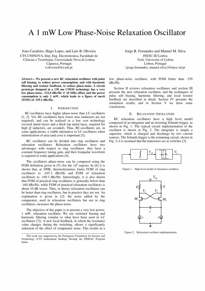
A 1 mW Low Phase-Noise Relaxation Oscillator
Joao Casaleiro, Hugo Lopes, and Luis B. Oliveira
CTS-UNINOVA, Dep. Eng. Electrotécnica, Faculdade de
Ciências e Tecnologia, Universidade Nova de Lisboa
Caparica, Portugal
Jorge R. Fernandes and Manuel M. Silva
INESC-ID Lisboa
Tech. University of Lisbon
Lisbon, Portugal
jorge.fernandes, [email protected]
Abstract— We present a new RC relaxation oscillator with pulse
self biasing, to reduce power consumption, and with harmonic
filtering and resistor feedback, to reduce phase-noise. A circuit
prototype designed in a 130 nm CMOS technology has a very
low phase-noise, -132.6 dBc/Hz @ 10 MHz offset, and the power
consumption is only 1 mW, which leads to a figure of merit
(FOM) of -159.1 dBc/Hz.
I. INTRODUCTION
RC-oscillators have higher phase-noise than LC-oscillators [1, 2]. Yet, RC-oscillators have lower area (inductors are not required), and can be realized in a low cost technology (several metal layers and a thick top metal layer, required for high Q inductors, are avoided). Thus, RC-oscillators are, in some applications, a viable alternative to LC-oscillators when minimization of area (and cost) is important [3].
RC oscillators can be divided into ring oscillators and relaxation oscillators. Relaxation oscillators have two advantages with respect to ring oscillators: they have a constant frequency tuning gain, and their triangular waveform is required in some applications [4].
The oscillators phase-noise can be compared using the
FOM definition given in [5] (for the 1/f2 region). In [6] it is
shown that, at 290K, thermodynamics limits FOM of ring
oscillators to -165.3 dBc/Hz and FOM of relaxation
oscillators to -169.1 dBc/Hz. Interestingly, it is also shown
that FOM of practical ring oscillators is generally below than
-160 dBc/Hz, while FOM of practical relaxation oscillators is
about 10 dB worse. Thus, in theory relaxation oscillators can
be better than ring oscillators, but in practice they are not. An
explanation is given in [2]: the noise added by the
comparator, used in relaxation oscillators but not in ring
oscillators, increases the phase-noise.
The objective of this paper is to present a very low power, 1 mW, relaxation oscillator. We use switched biasing and harmonic filtering (similar to what have been used in LC oscillators [7]). A new local feedback, in which the resistance value changes during the switching, allows a significantly reduction of the effect of comparator noise. This results in a
low phase-noise oscillator, with FOM better than -159 dBc/Hz.
Section II reviews relaxation oscillators and section III presents the new relaxation oscillator, and the techniques of pulse self biasing, harmonic filtering, and local resistor feedback are described in detail. Section IV presents the simulation results, and in Section V we draw some conclusions.
II. RELAXATION OSCILLATORS
RC relaxation oscillators have a high level model composed of an integrator and an inverting Schmitt-trigger, as shown in Fig. 1. The typical circuit implementation of the oscillator is shown in Fig. 2. The integrator is simply a capacitor, which is charged and discharge by two current sources. The Schmitt-trigger is the remaining circuit, shown in Fig. 3; it is assumed that the transistors act as switches [3].
∫ intV stV
Figure 1. High level model of relaxation oscillator.
I
ddV
C
RR
I
2M1M
1V 2V
Figure 2. Relaxation oscillator implementation.
This work was supported by the Portuguese Foundation for Science and
Technology (CTS multiannual funding) through the PIDDAC Program
funds.
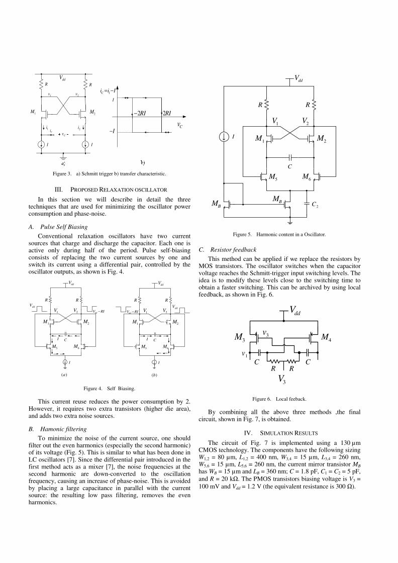
I I
1i 2i
R R
1v 2v
Cv
IiiC −= 1
I
I−
RI2− RI2
CvCi
ddV
1M2M
Figure 3. a) Schmitt trigger b) transfer characteristic.
III. PROPOSED RELAXATION OSCILLATOR
In this section we will describe in detail the three techniques that are used for minimizing the oscillator power consumption and phase-noise.
A. Pulse Self Biasing
Conventional relaxation oscillators have two current sources that charge and discharge the capacitor. Each one is active only during half of the period. Pulse self-biasing consists of replacing the two current sources by one and switch its current using a differential pair, controlled by the oscillator outputs, as shown is Fig. 4.
m
C
2M1M
I
5M 6M
2V1V
RR
ddV
RIVdd −
I
ddV
m
C
2M1M
I
5M 6M
2V1V
RR
RIVdd −
I
ddV
ddV
)(a )(b
Figure 4. Self Biasing.
This current reuse reduces the power consumption by 2. However, it requires two extra transistors (higher die area), and adds two extra noise sources.
B. Hamonic filtering
To minimize the noise of the current source, one should filter out the even harmonics (especially the second harmonic) of its voltage (Fig. 5). This is similar to what has been done in LC oscillators [7]. Since the differential pair introduced in the first method acts as a mixer [7], the noise frequencies at the second harmonic are down-converted to the oscillation frequency, causing an increase of phase-noise. This is avoided by placing a large capacitance in parallel with the current source: the resulting low pass filtering, removes the even harmonics.
C
2M1M
5M 6M
2V1V
RR
ddV
2CBM
BM
I
Figure 5. Harmonic content in a Oscillator.
C. Resistor feedback
This method can be applied if we replace the resistors by MOS transistors. The oscillator switches when the capacitor voltage reaches the Schmitt-trigger input switching levels. The idea is to modify these levels close to the switching time to obtain a faster switching. This can be archived by using local feedback, as shown in Fig. 6.
3V
ddV
3M 4M
C CR R
3v
1v
Figure 6. Local feeback.
By combining all the above three methods ,the final circuit, shown in Fig. 7, is obtained.
IV. SIMULATION RESULTS
The circuit of Fig. 7 is implemented using a 130 µm CMOS technology. The components have the following sizing W1,2 = 80 µm, L1,2 = 400 nm, W3,4 = 15 µm, L3,4 = 260 nm, W5,6 = 15 µm, L5,6 = 260 nm, the current mirror transistor MB has WB = 15 µm and LB = 360 nm; C = 1.8 pF, C1 = C2 = 5 pF,
and R = 20 kΩ. The PMOS transistors biasing voltage is V3 =
100 mV and Vdd = 1.2 V (the equivalent resistance is 300 Ω).
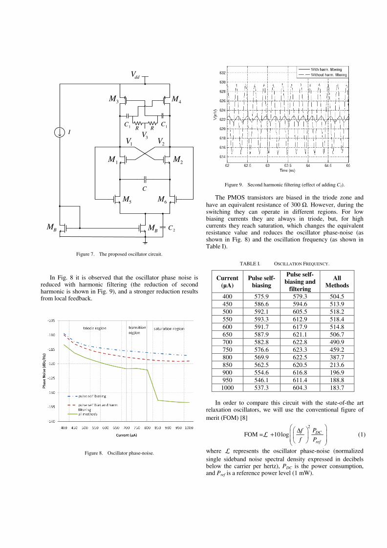
3V
3M4M
1CR R
C
2M1M
I
5M 6M
2V1V
ddV
1C
2CBMBM
Figure 7. The proposed oscillator circuit.
In Fig. 8 it is observed that the oscillator phase noise is reduced with harmonic filtering (the reduction of second harmonic is shown in Fig. 9), and a stronger reduction results from local feedback.
Figure 8. Oscillator phase-noise.
Figure 9. Second harmonic filtering (effect of adding C2).
The PMOS transistors are biased in the triode zone and
have an equivalent resistance of 300 Ω. However, during the switching they can operate in different regions. For low biasing currents they are always in triode, but, for high currents they reach saturation, which changes the equivalent resistance value and reduces the oscillator phase-noise (as shown in Fig. 8) and the oscillation frequency (as shown in Table I).
TABLE I. OSCILLATION FREQUENCY.
Current
(µA)
Pulse self-
biasing
Pulse self-
biasing and
filtering
All
Methods
400 575.9 579.3 504.5
450 586.6 594.6 513.9
500 592.1 605.5 518.2
550 593.3 612.9 518.4
600 591.7 617.9 514.8
650 587.9 621.1 506.7
700 582.8 622.8 490.9
750 576.6 623.3 459.2
800 569.9 622.5 387.7
850 562.5 620.5 213.6
900 554.6 616.8 196.9
950 546.1 611.4 188.8
1000 537.3 604.3 183.7
In order to compare this circuit with the state-of-the art relaxation oscillators, we will use the conventional figure of
merit (FOM) [8]
FOM =L
2
10log DC
ref
Pf
f P
∆ +
(1)
where L represents the oscillator phase-noise (normalized
single sideband noise spectral density expressed in decibels below the carrier per hertz), PDC is the power consumption, and Pref is a reference power level (1 mW).
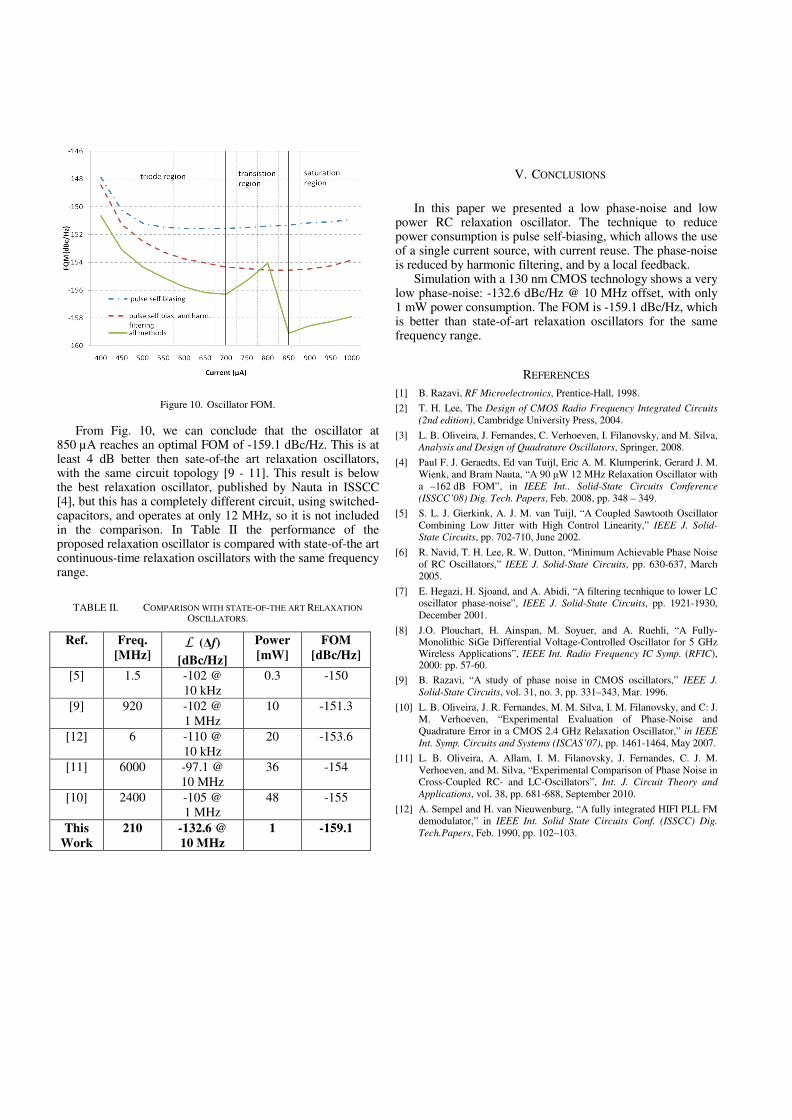
Figure 10. Oscillator FOM.
From Fig. 10, we can conclude that the oscillator at 850 µA reaches an optimal FOM of -159.1 dBc/Hz. This is at least 4 dB better then sate-of-the art relaxation oscillators, with the same circuit topology [9 - 11]. This result is below the best relaxation oscillator, published by Nauta in ISSCC [4], but this has a completely different circuit, using switched-capacitors, and operates at only 12 MHz, so it is not included in the comparison. In Table II the performance of the proposed relaxation oscillator is compared with state-of-the art continuous-time relaxation oscillators with the same frequency range.
TABLE II. COMPARISON WITH STATE-OF-THE ART RELAXATION
OSCILLATORS.
Ref. Freq.
[MHz] L (∆f)
[dBc/Hz]
Power
[mW]
FOM
[dBc/Hz]
[5] 1.5 -102 @
10 kHz
0.3 -150
[9] 920 -102 @
1 MHz
10 -151.3
[12] 6 -110 @
10 kHz
20 -153.6
[11] 6000 -97.1 @
10 MHz
36 -154
[10] 2400 -105 @
1 MHz
48 -155
This
Work
210 -132.6 @
10 MHz
1 -159.1
V. CONCLUSIONS
In this paper we presented a low phase-noise and low
power RC relaxation oscillator. The technique to reduce power consumption is pulse self-biasing, which allows the use of a single current source, with current reuse. The phase-noise is reduced by harmonic filtering, and by a local feedback.
Simulation with a 130 nm CMOS technology shows a very low phase-noise: -132.6 dBc/Hz @ 10 MHz offset, with only 1 mW power consumption. The FOM is -159.1 dBc/Hz, which is better than state-of-art relaxation oscillators for the same frequency range.
REFERENCES
[1] B. Razavi, RF Microelectronics, Prentice-Hall, 1998.
[2] T. H. Lee, The Design of CMOS Radio Frequency Integrated Circuits
(2nd edition), Cambridge University Press, 2004.
[3] L. B. Oliveira, J. Fernandes, C. Verhoeven, I. Filanovsky, and M. Silva,
Analysis and Design of Quadrature Oscillators, Springer, 2008.
[4] Paul F. J. Geraedts, Ed van Tuijl, Eric A. M. Klumperink, Gerard J. M.
Wienk, and Bram Nauta, “A 90 µW 12 MHz Relaxation Oscillator with
a –162 dB FOM”, in IEEE Int.. Solid-State Circuits Conference
(ISSCC’08) Dig. Tech. Papers, Feb. 2008, pp. 348 – 349.
[5] S. L. J. Gierkink, A. J. M. van Tuijl, “A Coupled Sawtooth Oscillator
Combining Low Jitter with High Control Linearity,” IEEE J. Solid-
State Circuits, pp. 702-710, June 2002.
[6] R. Navid, T. H. Lee, R. W. Dutton, “Minimum Achievable Phase Noise
of RC Oscillators,” IEEE J. Solid-State Circuits, pp. 630-637, March
2005.
[7] E. Hegazi, H. Sjoand, and A. Abidi, “A filtering tecnhique to lower LC
oscillator phase-noise”, IEEE J. Solid-State Circuits, pp. 1921-1930,
December 2001.
[8] J.O. Plouchart, H. Ainspan, M. Soyuer, and A. Ruehli, “A Fully-Monolithic SiGe Differential Voltage-Controlled Oscillator for 5 GHz Wireless Applications”, IEEE Int. Radio Frequency IC Symp. (RFIC), 2000: pp. 57-60.
[9] B. Razavi, “A study of phase noise in CMOS oscillators,” IEEE J.
Solid-State Circuits, vol. 31, no. 3, pp. 331–343, Mar. 1996.
[10] L. B. Oliveira, J. R. Fernandes, M. M. Silva, I. M. Filanovsky, and C: J.
M. Verhoeven, “Experimental Evaluation of Phase-Noise and
Quadrature Error in a CMOS 2.4 GHz Relaxation Oscillator,” in IEEE
Int. Symp. Circuits and Systems (ISCAS’07), pp. 1461-1464, May 2007.
[11] L. B. Oliveira, A. Allam, I. M. Filanovsky, J. Fernandes, C. J. M.
Verhoeven, and M. Silva, “Experimental Comparison of Phase Noise in
Cross-Coupled RC- and LC-Oscillators”, Int. J. Circuit Theory and
Applications, vol. 38, pp. 681-688, September 2010.
[12] A. Sempel and H. van Nieuwenburg, “A fully integrated HIFI PLL FM
demodulator,” in IEEE Int. Solid State Circuits Conf. (ISSCC) Dig.
Tech.Papers, Feb. 1990, pp. 102–103.
Bibliography
[1] J. Casaleiro, H. F. Lopes, L. B. Oliveira, and I. Filanovsky,
Cmos coupled multivibrators for wmts applications, Mixed
Design of Integrated Circuits and Systems (MIXDES), 2010
Proceedings of the 17th International Conference, pp. 231
236, jun. 2010.
[2] C. Dias, Osciladores de rádio frequência em quadratura com
acoplamento capacitivo, Master's thesis, Faculdade de Ciên-
cias e Tecnologia ( UNL ), 2009.
[3] I. Filanovsky, L. Oliveira, and J. Fernandes, Wide tuning
range quadrature vco using coupled multivibrators, Mixed
Design of Integrated Circuits Systems, 2009. MIXDES '09.
MIXDES-16th International Conference, pp. 341 344, jun.
2009.
117
Bibliography 118
[4] I. Finvers and I. Filanovsky, Analysis of a source-coupled
cmos multivibrator, Circuits and Systems, IEEE Transac-
tions on, vol. 35, no. 9, pp. 1182 1185, sep. 1988.
[5] A. Gerosa, S. Solda, A. Bevilacqua, D. Vogrig, and A. Ne-
viani, A digitally programmable ring oscillator in the UWB
range, Circuits and Systems (ISCAS), Proceedings of 2010
IEEE International Symposium on, pp. 1101 1104, may.
2010.
[6] E. Hegazi, H. Sjoland, and A. Abidi, A ltering technique
to lower lc oscillator phase noise, Solid-State Circuits, IEEE
Journal of, vol. 36, no. 12, pp. 1921 1930, dec. 2001.
[7] D. Johns and K. Martin, Analysis Integrated Circuit Design.
Wiley, 1996.
[8] T. Lee and A. Hajimiri, Oscillator phase noise: a tutorial,
Solid-State Circuits, IEEE Journal of, vol. 35, no. 3, pp. 326
336, mar. 2000.
[9] D. Leeson, A simple model of feedback oscillator noise spec-
trum, Proceedings of the IEEE, vol. 54, no. 2, pp. 329 330,
feb. 1966.
Bibliography 119
[10] L. B. Oliveira, J. R. Fernandes, I. M. Filanovsky, C. J. Ver-
hoeven, and M. M. Silva, Analysis and Design of Quadrature
Oscillators, Springer, Ed. Springer, 2008.
[11] L. B. Oliveira, E. T. Snelling, J. R. Fernandes, and M. M.
Silva, An inductorless cmos quadrature oscillator continu-
ously tuneable from 3.1 to 10.6?ghz, 2009.
[12] L. B. Oliveira, C. van den Bos, J. R. Fernandes, C. J. M.
Verhoeven, and M. M. Silva, A 5 GHz quadrature relaxation
oscillator with mixing for improved testability or compact
front-end implementation, 2008.
[13] B. Razavi, RF Microelectronics, P. Hall, Ed. Prentice Hall,
1998.
[14] A. Rezayee and K. Martin, A coupled two-stage ring oscilla-
tor, Circuits and Systems, 2001. MWSCAS 2001. Proceed-
ings of the 44th IEEE 2001 Midwest Symposium on, vol. 2,
pp. 878 881 vol.2, 2001.
[15] A. Rofougaran, J. Rael, M. Rofougaran, and A. Abidi, A
900 mhz cmos lc-oscillator with quadrature outputs, Solid-
State Circuits Conference, 1996. Digest of Technical Papers.
Bibliography 120
42nd ISSCC., 1996 IEEE International, pp. 392 393, feb.
1996.
[16] U. L. Rohde, A. K. Poddar, and G. Bock, The Design
of Modern Microwave Oscillators for Wireless Applications.
Wiley-Interscience, 2005.
[17] B. Soltanian and P. Kinget, Tail current-shaping to improve
phase noise in lc voltage-controlled oscillators, Solid-State
Circuits, IEEE Journal of, vol. 41, no. 8, pp. 1792 1802,
aug. 2006.
[18] R. Tao and M. Barroth, Low power 10 GHz ring V CO
using source capacitively coupled current amplier in 0.12
µm CMOS technology, Electronics Letters, vol. 40, no. 23,
pp. 1484 1486, nov. 2004.
[19] R. Tao and M. Berroth, The design of 5 GHz voltage con-
trolled ring oscillator using source capacitively coupled cur-
rent amplier, Microwave Symposium Digest, 2003 IEEE
MTT-S International, vol. 1, pp. A109 A112 vol.1, jun.
2003.
Bibliography 121
[20] Y.-S. Tiao and M.-L. Sheu, Full range voltage-controlled
ring oscillator in 0.18 µm CMOS for low-voltage operation,
Electronics Letters, vol. 46, no. 1, pp. 30 32, jan. 2010.
[21] M. Tiebout, Low Power VCO Design in CMOS. Springer,
2006.
[22] T. Tille, J. Sauerbrey, and D. Schmitt-Landsiedel, A low-
voltage mosfet-only sigma; delta; modulator for speech band
applications using depletion-mode mos-capacitors in com-
bined series and parallel compensation, Circuits and Sys-
tems, 2001. ISCAS 2001. The 2001 IEEE International Sym-
posium on, vol. 1, pp. 376 379 vol. 1, may. 2001.
[23] P. Tortoti, D. Guermandi, M. Guermandi, E. Franchi, and
A. Gnudi, Quadrature vcos based on direct second harmonic
locking: Theoretical analysis and experiment validation,
International Journal of Circuit Theory and Applications,
2009.
[24] A. Valero-Lopez, S. T. Moon, and E. Sanchez-Sinencio, Self-
calibrated quadrature generator for wlan multistandard fre-
quency synthesizer, Solid-State Circuits, IEEE Journal of,
vol. 41, no. 5, pp. 1031 1041, may. 2006.
Bibliography 122
[25] R. J. van de Plassche, J. H. Huijsing, and W. M. Sansen,
Analog Circuit Design: RF Analog-to-Digital Converters;
Sensor and Actuator Interfaces; Low-Noise Oscillators,
PLLs and Synthesizers, K. A. Publishers, Ed. Kluwer Aca-
demic Publishers, 1997.
[26] J. van der Tang and D. Kasperkovitz, Oscillator design
eciency: a new gure of merit for oscillator benchmark-
ing, Circuits and Systems, 2000. Proceedings. ISCAS 2000
Geneva. The 2000 IEEE International Symposium on, vol. 2,
pp. 533 536 vol.2, 2000.
[27] J. van der Tang, D. Kasperkovitz, and A. van Roermund,
High-Frequency Oscillator Design for Integrated Tranceivers.
Kluwer Academic Publishers, 2005.
[28] S. yeop Lee, S. Amakawa, N. Ishihara, and K. Masu, Low-
phase-noise wide-frequency-range ring-VCO-based scalable
PLL with subharmonic injection locking in 0.18 µm CMOS,
Microwave Symposium Digest (MTT), 2010 IEEE MTT-S
International, pp. 1178 1181, may. 2010.


![Two integrator loop quadrature oscillators: A review · Current feedback opera- ... [14] or the two output * Tel.: +20 27355482/35678822. E-mail address: asoliman@ieee.org. 2090-1232](https://static.documents.pub/doc/80x56/5f15a870f744b45df2101ffb/two-integrator-loop-quadrature-oscillators-a-review-current-feedback-opera-.jpg)


