General Description The MAX14838/MAX14839 24V/100mA drivers are optimized for use in industrial sensors. These devices integrate all of the high-voltage (24V) circuitry commonly found in industrial sensors, including a configurable PNP/ NPN/push-pull driver and an integrated linear regulator that meets common sensor power requirements. The MAX14838/MAX14839 are pin-configurable. Logic inputs allow the driver to be configured for high-side (PNP), low-side (NPN), or push-pull operation. An additional input allows the user to select between normal- ly-open and normally-closed logic. The MAX14838 features an onboard 5V linear regulator, while the MAX14839 features a 3.3V linear regulator. Each device includes two LED drivers for visual feedback. One LED driver reflects the output logic status and the other is a general-purpose driver that can be used to signal a fault condition. The DO output, supply (V CC ), and ground (GND) pins are reverse polarity-protected and are protected against IEC ESD and surge events. The MAX14838 and MAX14839 operate from a wide sup- ply range and are available in a 12-pin TDFN-EP package (3mm x 3mm) or a 12-bump wafer-level package (WLP) (2.1mm x 1.6mm) and operate over the -40°C to +105°C temperature range. Benefits and Features ● High Configurability Simplifies Design • Pin-Selectable High-Side (PNP), Low-Side (NPN), or Push-Pull Driver • Pin-Configurable NO/NC Logic ● Integrated Protection Provides Robust Sensor Solutions • Reverse-Polarity Protection on DO, V CC , and GND • 4.75V to 34V Supply Range (MAX14839) • Driver is Short-Circuit Protected • FAULT Output for Fault Indication • V CC Hot Plug Protection • Thermal Shutdown Protection • ±1kV/500Ω Surge Protection • ±8kV IEC 61000-4-2 Air Gap ESD Protection • ±6kV IEC 61000-4-2 Contact ESD Protection • -40°C to +105°C Temperature Range ● Fast Turn-Off of Inductive Loads Up to 1.5H ● Saves Space on Board • Available in 12-Pin TDFN-EP (3mm x 3mm) or 12-Bump WLP (2.1mm x 1.6mm) • Dual Integrated 2mA LED Drivers Applications ● Industry Binary Sensors ● Proximity Switches ● Capacitive and Inductive Sensors Ordering Information appears at end of data sheet. 19-7465; Rev 2; 6/15 VCC NPN DIN MAX14838 MAX14839 FAULT 100nF DO GND 24V OUT GND LEDS LED2 LDO LED2IN PP NO SENSOR AFE 100nF Typical Application Circuit MAX14838/MAX14839 24V Pin-Configurable Industrial Sensor Output Drivers EVALUATION KIT AVAILABLE
Transcript
General DescriptionThe MAX14838/MAX14839 24V/100mA drivers are optimized for use in industrial sensors. These devices integrate all of the high-voltage (24V) circuitry commonly found in industrial sensors, including a configurable PNP/NPN/push-pull driver and an integrated linear regulator that meets common sensor power requirements.The MAX14838/MAX14839 are pin-configurable. Logic inputs allow the driver to be configured for high-side (PNP), low-side (NPN), or push-pull operation. An additional input allows the user to select between normal-ly-open and normally-closed logic.The MAX14838 features an onboard 5V linear regulator, while the MAX14839 features a 3.3V linear regulator.Each device includes two LED drivers for visual feedback. One LED driver reflects the output logic status and the other is a general-purpose driver that can be used to signal a fault condition.The DO output, supply (VCC), and ground (GND) pins are reverse polarity-protected and are protected against IEC ESD and surge events.The MAX14838 and MAX14839 operate from a wide sup-ply range and are available in a 12-pin TDFN-EP package (3mm x 3mm) or a 12-bump wafer-level package (WLP) (2.1mm x 1.6mm) and operate over the -40°C to +105°C temperature range.
Benefits and Features High Configurability Simplifies Design
• Pin-Selectable High-Side (PNP), Low-Side (NPN), or Push-Pull Driver
Solutions• Reverse-Polarity Protection on DO, VCC, and GND• 4.75V to 34V Supply Range (MAX14839)• Driver is Short-Circuit Protected• FAULT Output for Fault Indication• VCC Hot Plug Protection• Thermal Shutdown Protection• ±1kV/500Ω Surge Protection• ±8kV IEC 61000-4-2 Air Gap ESD Protection• ±6kV IEC 61000-4-2 Contact ESD Protection• -40°C to +105°C Temperature Range
Fast Turn-Off of Inductive Loads Up to 1.5H Saves Space on Board
• Available in 12-Pin TDFN-EP (3mm x 3mm) or 12-Bump WLP (2.1mm x 1.6mm)
• Dual Integrated 2mA LED Drivers
Applications Industry Binary Sensors Proximity Switches Capacitive and Inductive SensorsOrdering Information appears at end of data sheet.
(All voltages referenced to GND, unless otherwise specified.)VCC .........................................................................-36V to +36VLDO .........................................................................-0.3V to +6VDO ...........................................................Higher of (VCC - 36V) and -36V Lower of (VCC + 36V) and +36VDIN, NPN, PP, NO, LDO2IN, FAULT .......................-0.3V to +6V LEDS, LED2 ....... -0.3V to the higher of (VCC - 0.3V) and +0.3V
Continuous Power Dissipation (TA = +70°C) Multiple-Layer Board
(derate at 24.4mW/°C above +70°C) ........................1950mWOperating Temperature Range ......................... -40°C to +105°CJunction Temperature ...................................................... +150ºCStorage Temperature Range .............................-65ºC to +150°CSolder Temperature (Reflow) .........................................+260°C
(VCC = 4.75V to 34V (MAX14839), VCC = 7V to 34V (MAX14838), unless otherwise noted. VGND = 0V. All logic inputs are VLDO or GND. TA = TMIN to TMAX. Typical values are at VCC = 24V, TA = +25°C) (Notes 2, 3)
Note 1: Package thermal resistances were obtained using the method described in JEDEC specification JESD51-7, using a four-layer board. For detailed information on package thermal considerations, refer to www.maximintegrated.com/thermal-tutorial.
PARAMETER SYMBOL CONDITIONS MIN TYP MAX UNITSPOWER SUPPLY
Supply Voltage VCCMAX14839 4.75 34
VMAX14838 7 34
Supply Current ICC
VCC = 24V, no external load on LDO, DO is open-drain or push-pull mode, no load on DO, LEDS, and LED2 off
Stresses beyond those listed under “Absolute Maximum Ratings” may cause permanent damage to the device. These are stress ratings only, and functional operation of the device at these or any other conditions beyond those indicated in the operational sections of the specifications is not implied. Exposure to absolute maximum rating conditions for extended periods may affect device reliability.
Package Thermal Characteristics
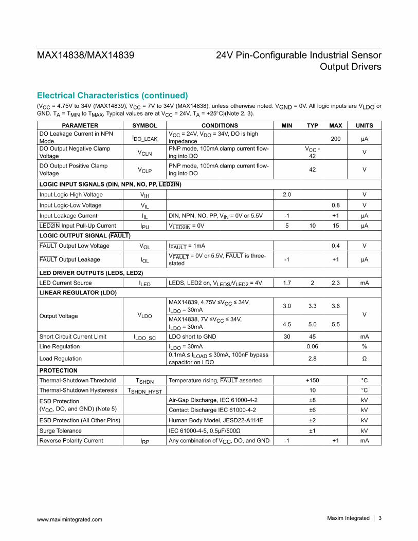
Electrical Characteristics
(VCC = 4.75V to 34V (MAX14839), VCC = 7V to 34V (MAX14838), unless otherwise noted. VGND = 0V. All logic inputs are VLDO or GND. TA = TMIN to TMAX, Typical values are at VCC = 24V, TA = +25°C)(Note 2, 3).
PARAMETER SYMBOL CONDITIONS MIN TYP MAX UNITSDO Leakage Current in NPN Mode IDO_LEAK
VCC = 24V, VDO = 34V, DO is high impedance 200 μA
DO Output Negative Clamp Voltage VCLN
PNP mode, 100mA clamp current flow-ing into DO
VCC - 42 V
DO Output Positive Clamp Voltage VCLP
PNP mode, 100mA clamp current flow-ing into DO 42 V
LOGIC INPUT SIGNALS (DIN, NPN, NO, PP, LED2IN)
Input Logic-High Voltage VIH 2.0 V
Input Logic-Low Voltage VIL 0.8 V
Input Leakage Current IIL DIN, NPN, NO, PP, VIN = 0V or 5.5V -1 +1 μA
(VCC = 4.75V to 34V (MAX14839), VCC = 7V to 34V (MAX14838), unless otherwise noted. VGND = 0V, All logic inputs are VLDO or GND. TA = TMIN to TMAX, Typical values are at VCC = 24V, TA = +25°C)(Note 2, 3)
Note 2: All units are production tested at TA = +25°C. Specifications over temperature are guaranteed by design.Note 3: Currents into the device as positive; all currents out of the device are negative. All voltages are referenced to ground, unless
otherwise noted.Note 4: See the DO Short-Circuit and Overcurrent Protection section for detailed information.Note 5: ESD protection for VCC is achieved only with an external capacitor connected from VCC to GND. Connect 100nF capacitor
between VCC and GND for air-gap and contact discharge ESD.
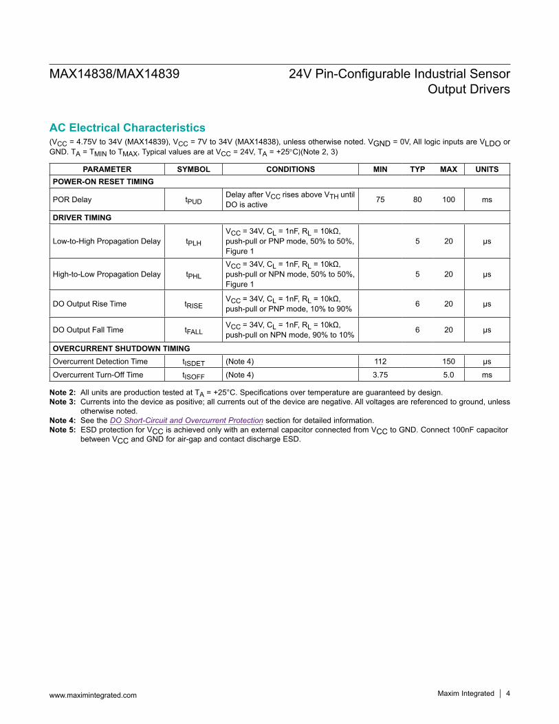
PARAMETER SYMBOL CONDITIONS MIN TYP MAX UNITSPOWER-ON RESET TIMING
POR Delay tPUDDelay after VCC rises above VTH until DO is active 75 80 100 ms
DRIVER TIMING
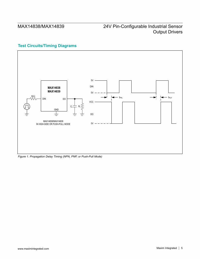
Low-to-High Propagation Delay tPLH
VCC = 34V, CL = 1nF, RL = 10kΩ, push-pull or PNP mode, 50% to 50%, Figure 1
5 20 μs
High-to-Low Propagation Delay tPHL
VCC = 34V, CL = 1nF, RL = 10kΩ, push-pull or NPN mode, 50% to 50%, Figure 1
5 20 μs
DO Output Rise Time tRISEVCC = 34V, CL = 1nF, RL = 10kΩ, push-pull or PNP mode, 10% to 90% 6 20 μs
DO Output Fall Time tFALLVCC = 34V, CL = 1nF, RL = 10kΩ, push-pull on NPN mode, 90% to 10% 6 20 μs
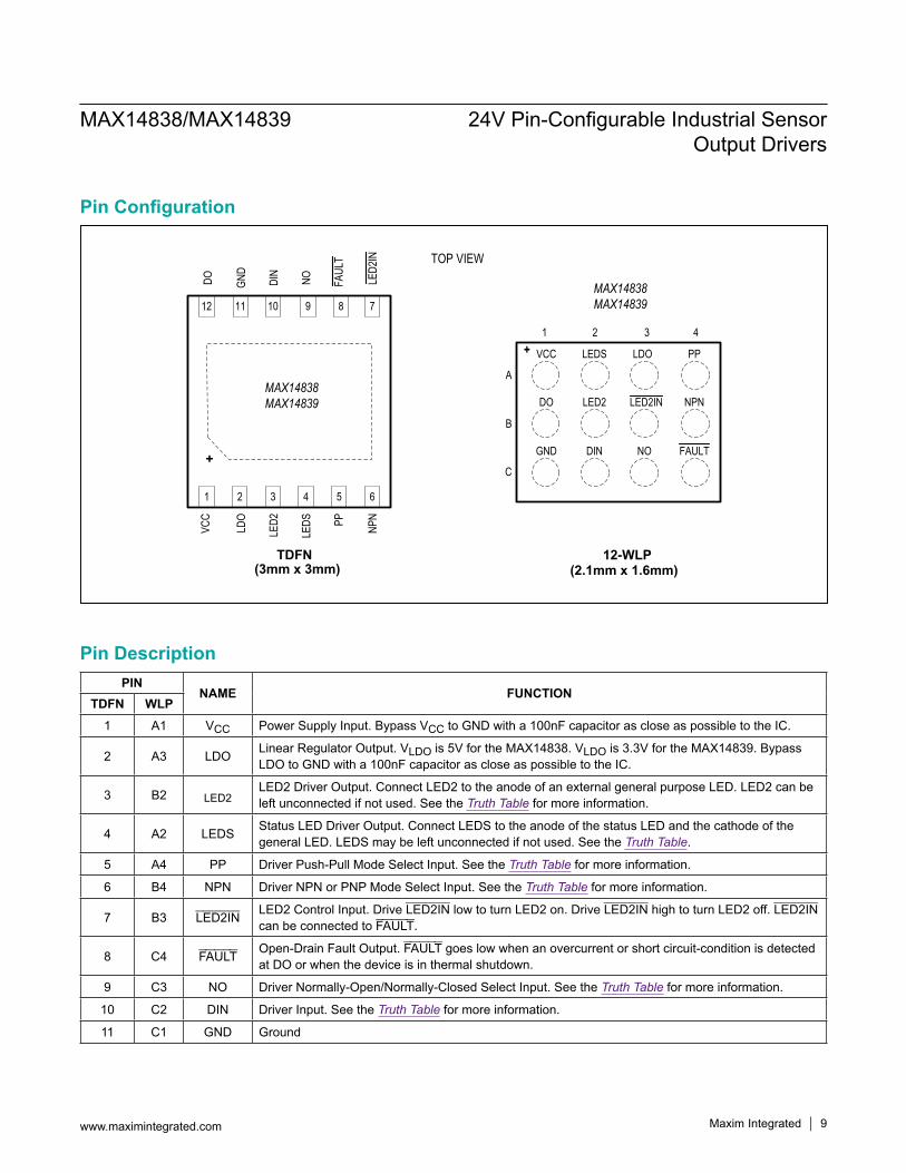
TDFN WLP1 A1 VCC Power Supply Input. Bypass VCC to GND with a 100nF capacitor as close as possible to the IC.
2 A3 LDO Linear Regulator Output. VLDO is 5V for the MAX14838. VLDO is 3.3V for the MAX14839. Bypass LDO to GND with a 100nF capacitor as close as possible to the IC.
3 B2 LED2LED2 Driver Output. Connect LED2 to the anode of an external general purpose LED. LED2 can be left unconnected if not used. See the Truth Table for more information.
4 A2 LEDS Status LED Driver Output. Connect LEDS to the anode of the status LED and the cathode of the general LED. LEDS may be left unconnected if not used. See the Truth Table.
5 A4 PP Driver Push-Pull Mode Select Input. See the Truth Table for more information.
6 B4 NPN Driver NPN or PNP Mode Select Input. See the Truth Table for more information.
7 B3 LED2IN LED2 Control Input. Drive LED2IN low to turn LED2 on. Drive LED2IN high to turn LED2 off. LED2IN can be connected to FAULT.
8 C4 FAULT Open-Drain Fault Output. FAULT goes low when an overcurrent or short circuit-condition is detected at DO or when the device is in thermal shutdown.
9 C3 NO Driver Normally-Open/Normally-Closed Select Input. See the Truth Table for more information.
10 C2 DIN Driver Input. See the Truth Table for more information.
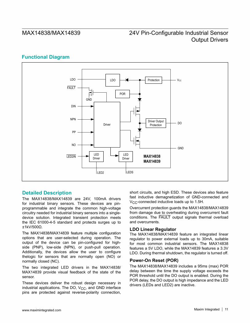
Detailed DescriptionThe MAX14838/MAX14839 are 24V, 100mA drivers for industrial binary sensors. These devices are pin-programmable and integrate the common high-voltage circuitry needed for industrial binary sensors into a single-device solution. Integrated transient protection meets the IEC 61000-4-5 standard and protects surges up to ±1kV/500Ω. The MAX14838/MAX14839 feature multiple configuration options that are user-selected during operation. The output of the device can be pin-configured for high-side (PNP), low-side (NPN), or push-pull operation. Additionally, the devices allow the user to configure thelogic for sensors that are normally open (NO) or normally closed (NC).The two integrated LED drivers in the MAX14838/MAX14839 provide visual feedback of the state of the sensor.These devices deliver the robust design necessary in industrial applications. The DO, VCC, and GND interface pins are protected against reverse-polarity connection,
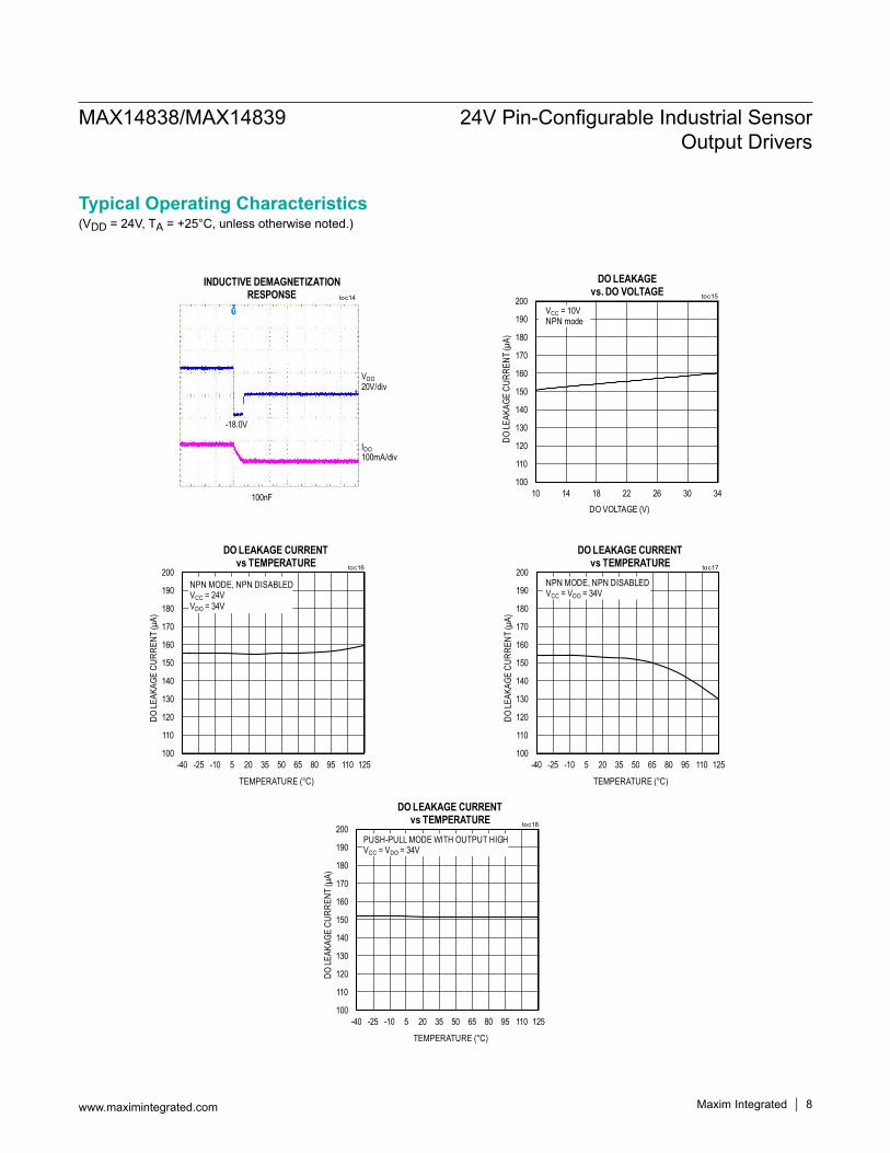
short circuits, and high ESD. These devices also feature fast inductive demagnetization of GND-connected and VCC-connected inductive loads up to 1.5H. Overcurrent protection guards the MAX14838/MAX14839 from damage due to overheating during overcurrent fault conditions. The FAULT output signals thermal overload and overcurrents.
LDO Linear RegulatorThe MAX14838/MAX14839 feature an integrated linear regulator to power external loads up to 30mA, suitable for most common industrial sensors. The MAX14838 features a 5V LDO, while the MAX14839 features a 3.3V LDO. During thermal shutdown, the regulator is turned off.
Power-On Reset (POR)The MAX14838/MAX14839 includes a 95ms (max) POR delay between the time the supply voltage exceeds the POR threshold until the DO output is enabled. During the POR delay, the DO output is high impedance and the LED drivers (LEDs and LED2) are inactive.
Reverse-Polarity ProtectionReverse-polarity protection is built into the MAX14838/MAX14839. Integrated circuitry protects the device against accidental reverse-polarity connections to the VCC, DO, and GND pins. During a reverse-polarity plugin event, the maximum current drawn through VCC, DO, or GND is 1mA. The maximum voltage between any of the pins must not exceed 36VDC at any time.
Voltage TransientsShort-duration voltage transients that rise above the absolute maximum rating of the VCC pin occur during ESD, burst, and hot plug events. The MAX14838/MAX14839 cannot be damaged with a 100nF bypass capacitor on the VCC line. Transients due to inductive kickback on DO when driving inductive loads up to 1.5H at 100mA or less can also bring the DO voltage above the absolute maximum rating, yet not damage the device. The absolute maximum ratings for VCC and DO should not be violated for any length of time by external sources.
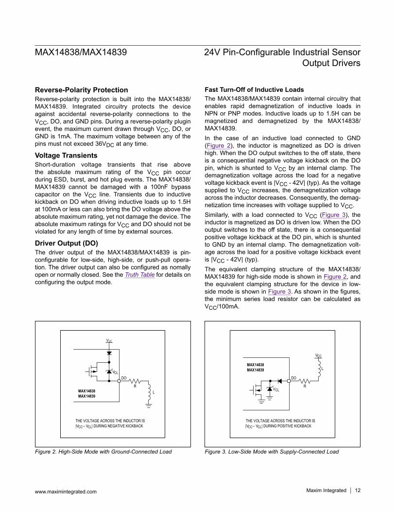
Driver Output (DO)The driver output of the MAX14838/MAX14839 is pin-configurable for low-side, high-side, or push-pull opera-tion. The driver output can also be configured as nomally open or normally closed. See the Truth Table for details on configuring the output mode.
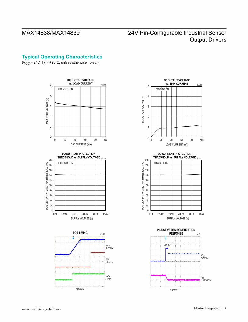
Fast Turn-Off of Inductive LoadsThe MAX14838/MAX14839 contain internal circuitry that enables rapid demagnetization of inductive loads in NPN or PNP modes. Inductive loads up to 1.5H can be magnetized and demagnetized by the MAX14838/MAX14839.In the case of an inductive load connected to GND (Figure 2), the inductor is magnetized as DO is driven high. When the DO output switches to the off state, there is a consequential negative voltage kickback on the DO pin, which is shunted to VCC by an internal clamp. The demagnetization voltage across the load for a negative voltage kickback event is |VCC - 42V| (typ). As the voltage supplied to VCC increases, the demagnetization voltage across the inductor decreases. Consequently, the demag-netization time increases with voltage supplied to VCC.Similarly, with a load connected to VCC (Figure 3), the inductor is magnetized as DO is driven low. When the DO output switches to the off state, there is a consequential positive voltage kickback at the DO pin, which is shunted to GND by an internal clamp. The demagnetization volt-age across the load for a positive voltage kickback event is |VCC - 42V| (typ).The equivalent clamping structure of the MAX14838/MAX14839 for high-side mode is shown in Figure 2, and the equivalent clamping structure for the device in low-side mode is shown in Figure 3. As shown in the figures, the minimum series load resistor can be calculated as VCC/100mA.
Figure 2. High-Side Mode with Ground-Connected Load Figure 3. Low-Side Mode with Supply-Connected Load
VCL
MAX14838MAX14839
VCC
DO
R
THE VOLTAGE ACROSS THE INDUCTOR IS|VCC– VCL| DURING NEGATIVE KICKBACK
LVCL
MAX14838MAX14839
DO
R
THE VOLTAGE ACROSS THE INDUCTOR IS|VCC– VCL| DURING POSITIVE KICKBACK
Capacitive LoadsThe MAX14838/MAX14839 are capable of driving capaci-tive loads on the DO output. Assuming a pure capacitive load without series/parallel resistance, the maximum capacitance that can be charged can be calculated as:
CLOAD = [ICL x tISDET]/ VCCHigher capacitive loads can be driven if a series resis-tor is connected between the DO ouput and the load. Capacitive loads can be connected to ground or VCC.
DO Short-Circuit and Overcurrent ProtectionThe DO driver load current is actively limited to ICL (350mA, typ). When the DO load current exceeds the current protection threshold, IOC (145mA, typ), for a duration lon-ger than tISDET (130μs,typ), the DO driver is immediately turned off and enters autoretry mode. In autoretry mode, DO is turned off for tISOFF (4ms, typ) and then powered up for tISDET. If the short-circuit condition has not been removed, the cycle repeats. The device turns off for tISOFF, then back on for tISDET, reducing the overall power dissipation at DO.LED Output DriversThe MAX14838/MAX14839 allow the user to receive visual feedback of the state of the sensor using two LED driver outputs, LEDS and LED2. The LED drivers protect onboard LEDs against possible reverse-polarity connec-tions on the VCC supply.If LEDS and LED2 are used, connect as shown in the Typical Application Circuit. When using a low supply voltage, ensure that the sum of the two LED’s forward-voltage is less than 4V.If only LEDS is used, leave LED2IN and LED2 uncon-nected. If only LED2 is used, connect LEDS to ground.
General Purpose LED Driver (LED2)LED2 is a general-purpose LED driver output. LED2IN is the input for LED2. Pull LED2IN low to turn on the LED2 output. To configure LED2 as a visual fault indicator, connect LED2IN to FAULT.
Output Driver State Indicator (LEDS)The LEDS driver output signals the state of the DO driver. LEDS sources current when one DO output transistor is on in PNP or NPN mode. See Truth Table for more infor-mation. Thermal ShutdownThe MAX14838/MAX14839 includes integrated protec-tion against thermal overload. When the die temperature rises above +150°C (typ), the DO driver, LED drivers, and the linear regulator automatically turn off until the die temperature returns to a safe level.
Applications InformationBurst ProtectionTo improve false transitions during burst testing, connect a 4.7nF capacitor between DO and VCC and another between DO and GND.
Extended ESD ProtectionESD-protection structures are incorporated on all pins to protect against electrostatic discharges up to ±2kV (HBM)encountered during handling and assembly. VCC, DO, and GND are further protected against ESD up to ±12kV (Air-Gap Discharge), and ±8kV (Contact Discharge) with-out damage. The ESD structures withstand high ESD both in normal operation and when the device is pow-ered down. After an ESD event, the devices continue to function without latchup.
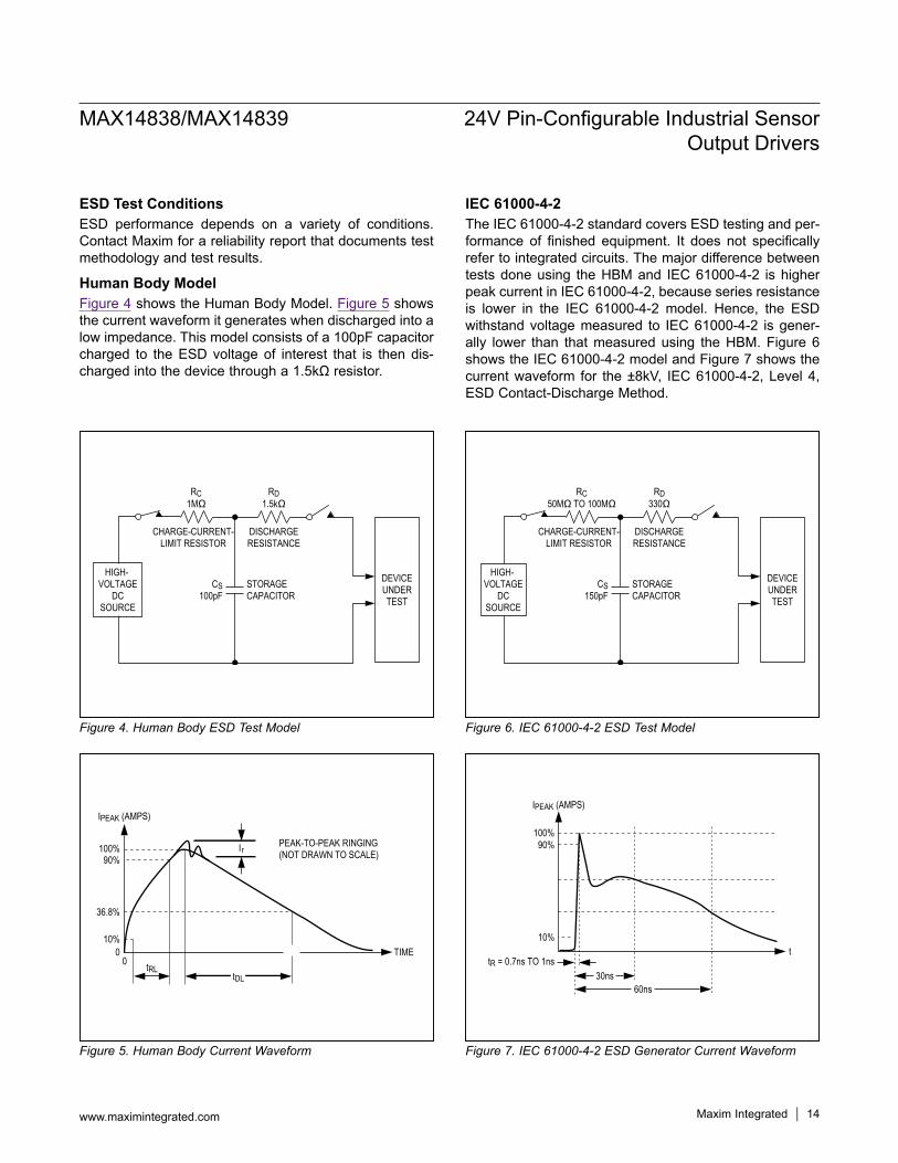
ESD Test ConditionsESD performance depends on a variety of conditions. Contact Maxim for a reliability report that documents test methodology and test results.
Human Body ModelFigure 4 shows the Human Body Model. Figure 5 shows the current waveform it generates when discharged into a low impedance. This model consists of a 100pF capacitor charged to the ESD voltage of interest that is then dis-charged into the device through a 1.5kΩ resistor.
IEC 61000-4-2The IEC 61000-4-2 standard covers ESD testing and per-formance of finished equipment. It does not specifically refer to integrated circuits. The major difference between tests done using the HBM and IEC 61000-4-2 is higher peak current in IEC 61000-4-2, because series resistance is lower in the IEC 61000-4-2 model. Hence, the ESD withstand voltage measured to IEC 61000-4-2 is gener-ally lower than that measured using the HBM. Figure 6 shows the IEC 61000-4-2 model and Figure 7 shows the current waveform for the ±8kV, IEC 61000-4-2, Level 4, ESD Contact-Discharge Method.
Figure 4. Human Body ESD Test Model
Figure 5. Human Body Current Waveform
Figure 6. IEC 61000-4-2 ESD Test Model
Figure 7. IEC 61000-4-2 ESD Generator Current Waveform
Package InformationFor the latest package outline information and land patterns (foot-prints), go to www.maximintegrated.com/packages. Note that a “+”, “#”, or “-” in the package code indicates RoHS status only. Package drawings may show a different suffix character, but the drawing pertains to the package regardless of RoHS status.
PACKAGE TYPE
PACKAGE CODE
OUTLINE NO.
LAND PATTERN NO.
12 TDFN-EP TD1233+1 21-0664 90-0397
12 WLP W121C2+1 21-0009Refer to
Application Note 1891
Ordering Information
PART LDO VOLTAGE
TEMP RANGE
PIN- PACKAGE
MAX14838GTC+ 5V -40°C to +105°C
12 TDFN-EP
MAX14838GWC+ 5V -40°C to +105°C
12-bump WLP
MAX14839GTC+ 3.3V -40°C to +105°C
12-TDFN-EP
MAX14839GWC+ 3.3V -40°C to +105C
12-bump WLP
+Denotes a lead(Pb)-free/RoHS-compliant package.*EP = Exposed pad
2 6/15 Updated TOC08 in the Typical Operating Characteristics section 7
Maxim Integrated cannot assume responsibility for use of any circuitry other than circuitry entirely embodied in a Maxim Integrated product. No circuit patent licenses are implied. Maxim Integrated reserves the right to change the circuitry and specifications without notice at any time. The parametric values (min and max limits) shown in the Electrical Characteristics table are guaranteed. Other parametric values quoted in this data sheet are provided for guidance.
Maxim Integrated and the Maxim Integrated logo are trademarks of Maxim Integrated Products, Inc.
For pricing, delivery, and ordering information, please contact Maxim Direct at 1-888-629-4642, or visit Maxim Integrated’s website at www.maximintegrated.com.