22
Memories and SRAM 1

Memories and SRAM
1
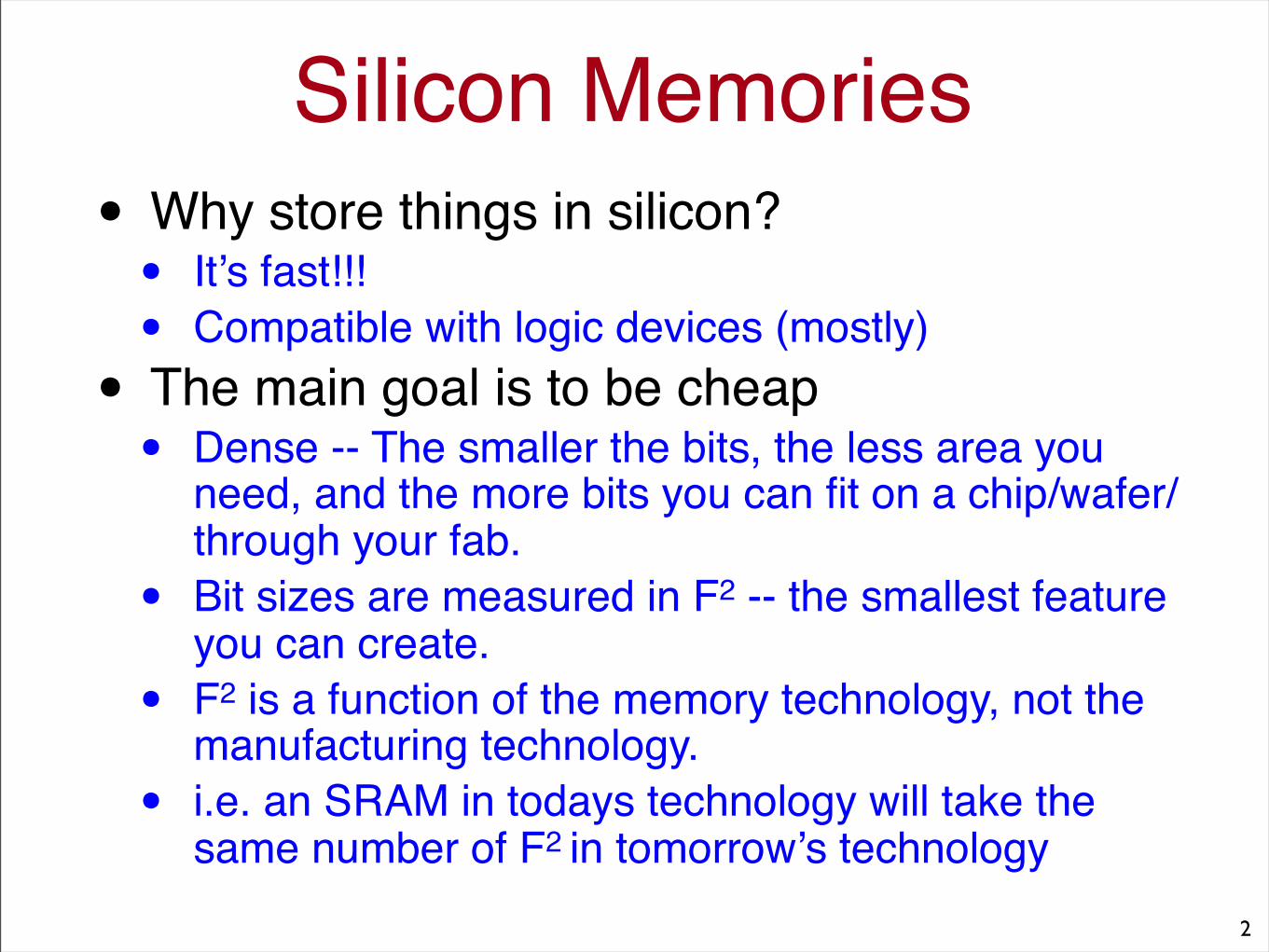
Silicon Memories• Why store things in silicon?• It’s fast!!!• Compatible with logic devices (mostly)• The main goal is to be cheap• Dense -- The smaller the bits, the less area you
need, and the more bits you can fit on a chip/wafer/through your fab.
• Bit sizes are measured in F2 -- the smallest feature you can create.
• F2 is a function of the memory technology, not the manufacturing technology.
• i.e. an SRAM in todays technology will take the same number of F2 in tomorrow’s technology
2
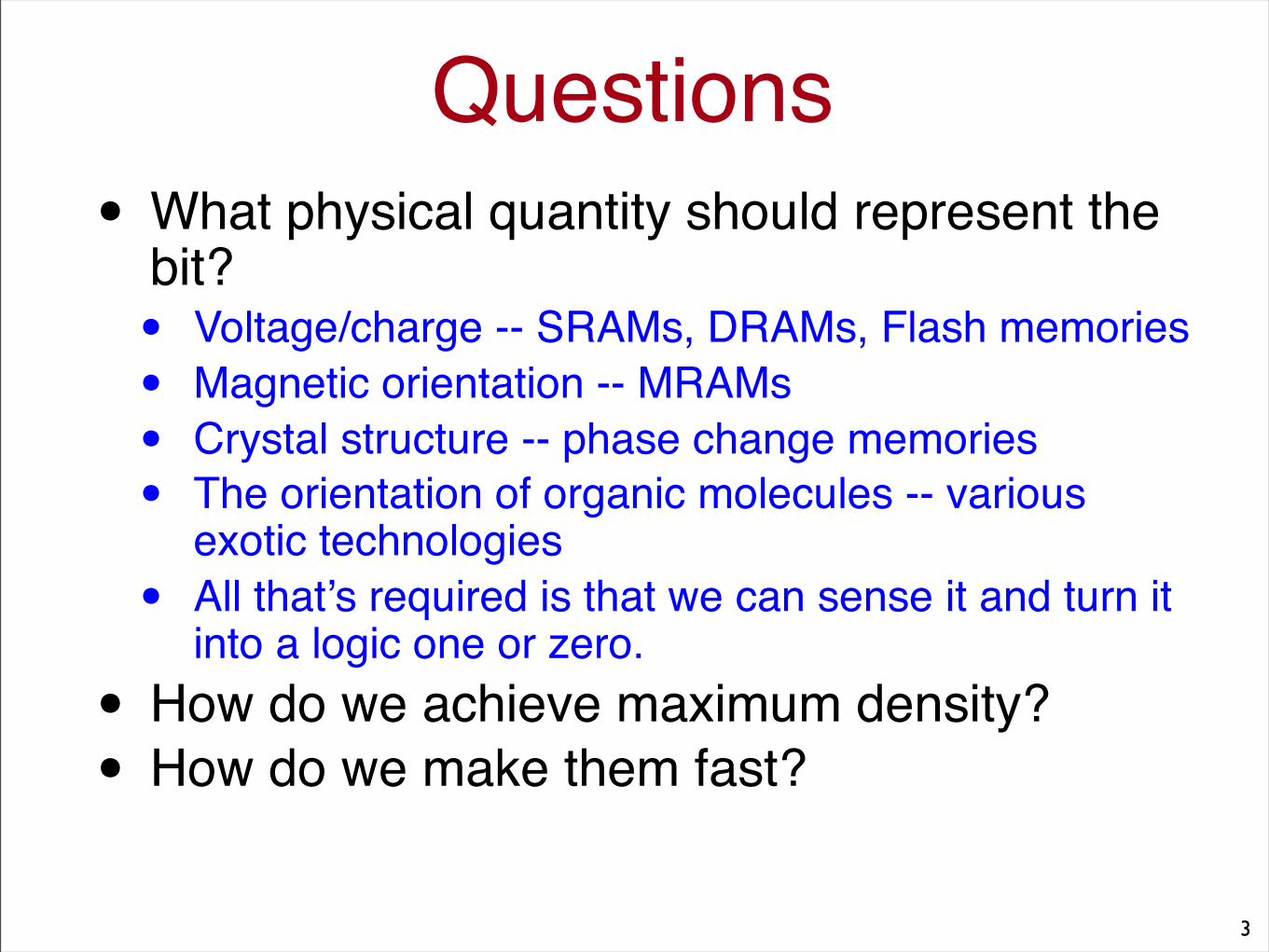
Questions• What physical quantity should represent the
bit?• Voltage/charge -- SRAMs, DRAMs, Flash memories• Magnetic orientation -- MRAMs• Crystal structure -- phase change memories• The orientation of organic molecules -- various
exotic technologies• All that’s required is that we can sense it and turn it
into a logic one or zero.• How do we achieve maximum density?• How do we make them fast?
3
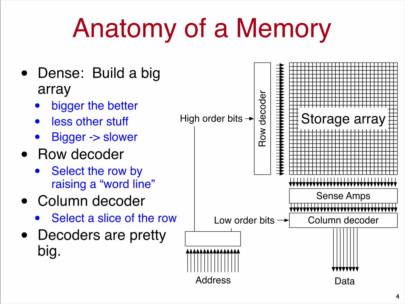
Anatomy of a Memory• Dense: Build a big
array• bigger the better• less other stuff• Bigger -> slower
• Row decoder• Select the row by
raising a “word line”
• Column decoder• Select a slice of the row
• Decoders are pretty big.
4
Row
decoder
Column decoder
Sense Amps
High order bits
Low order bits
Storage array
DataAddress
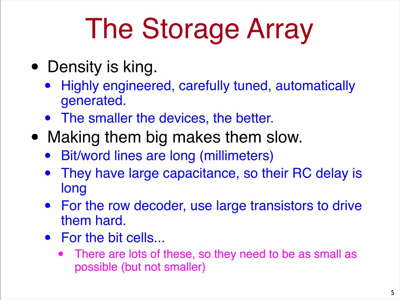
The Storage Array• Density is king.• Highly engineered, carefully tuned, automatically
generated.• The smaller the devices, the better.• Making them big makes them slow.• Bit/word lines are long (millimeters)• They have large capacitance, so their RC delay is
long• For the row decoder, use large transistors to drive
them hard. • For the bit cells...• There are lots of these, so they need to be as small as
possible (but not smaller)
5
Measuring Memory Density• We use a “technology independent” metric to measure
the inherent size of different memory cells.• F == the “feature size” == the smallest dimension a CMOS
process can create (e.g., the width of the narrowest wire).• In a 22nm process technology, F = 22nm.• F2 (F-squared) is the smallest 2D feature we can manufacture.
• A single bit of a given type of memory (e.g., SRAM or DRAM) requires a fixed number of F2 • This number doesn’t change with process technology.• e.g., NAND flash memory is 4F2 in 90nm and in 22nm.
• Using this metic is useful because the relative sizes of different memory technologies don’t change much, although absolute densities do.
6
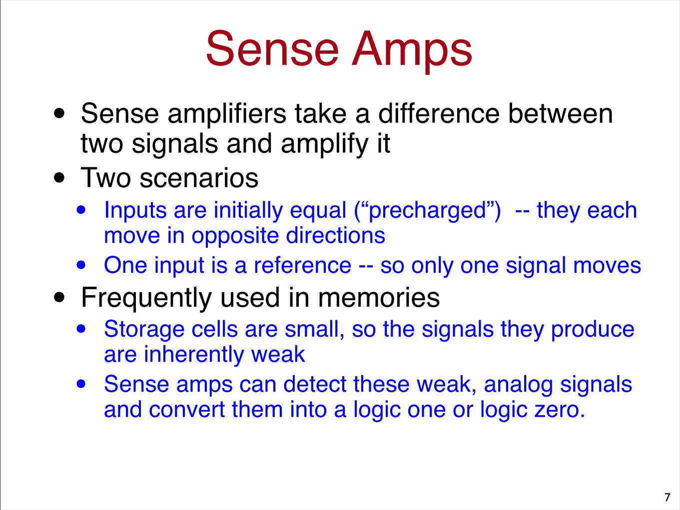
Sense Amps• Sense amplifiers take a difference between
two signals and amplify it• Two scenarios• Inputs are initially equal (“precharged”) -- they each
move in opposite directions• One input is a reference -- so only one signal moves• Frequently used in memories• Storage cells are small, so the signals they produce
are inherently weak• Sense amps can detect these weak, analog signals
and convert them into a logic one or logic zero.
7

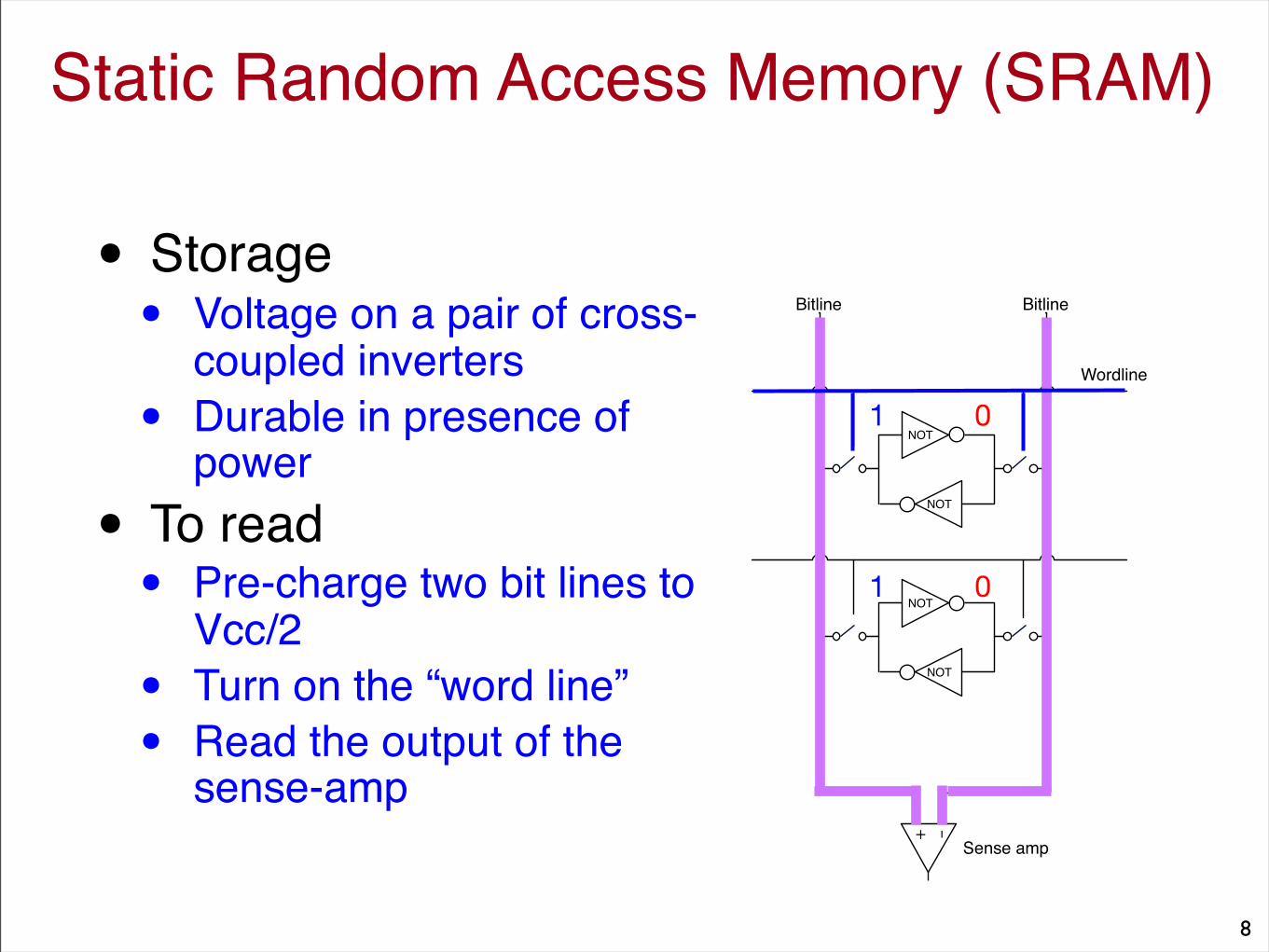
Static Random Access Memory (SRAM)
• Storage• Voltage on a pair of cross-
coupled inverters• Durable in presence of
power
• To read• Pre-charge two bit lines to
Vcc/2• Turn on the “word line”• Read the output of the
sense-amp
1 0NOT
NOT
Bitline Bitline
Wordline
NOT
NOT
-+
Sense amp
1 0
8

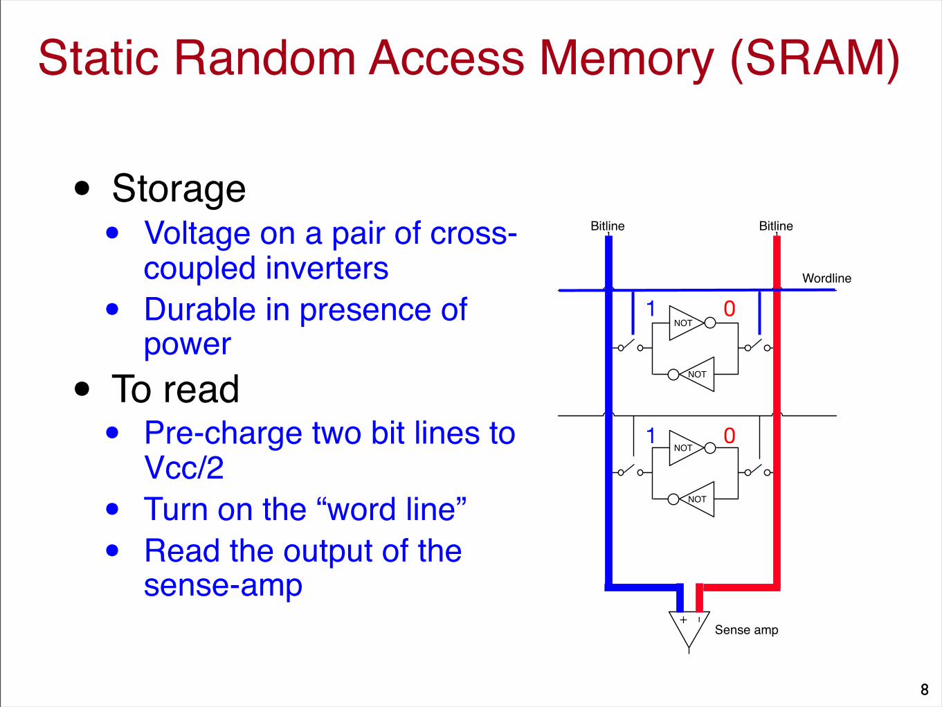
Static Random Access Memory (SRAM)
• Storage• Voltage on a pair of cross-
coupled inverters• Durable in presence of
power
• To read• Pre-charge two bit lines to
Vcc/2• Turn on the “word line”• Read the output of the
sense-amp
1 0NOT
NOT
Bitline Bitline
Wordline
NOT
NOT
-+
Sense amp
1 0
8
Static Random Access Memory (SRAM)
• Storage• Voltage on a pair of cross-
coupled inverters• Durable in presence of
power
• To read• Pre-charge two bit lines to
Vcc/2• Turn on the “word line”• Read the output of the
sense-amp
1 0NOT
NOT
Bitline Bitline
Wordline
NOT
NOT
-+
Sense amp
1 0
8
Static Random Access Memory (SRAM)
• Storage• Voltage on a pair of cross-
coupled inverters• Durable in presence of
power
• To read• Pre-charge two bit lines to
Vcc/2• Turn on the “word line”• Read the output of the
sense-amp
1 0NOT
NOT
Bitline Bitline
Wordline
NOT
NOT
-+
Sense amp
1 0
8

Static Random Access Memory (SRAM)
• Storage• Voltage on a pair of cross-
coupled inverters• Durable in presence of
power
• To read• Pre-charge two bit lines to
Vcc/2• Turn on the “word line”• Read the output of the
sense-amp
1 0NOT
NOT
Bitline Bitline
Wordline
NOT
NOT
-+
Sense amp
1 0
18

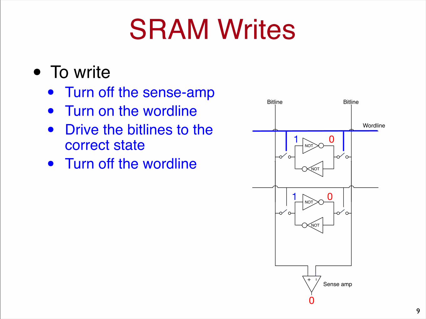
1 0
SRAM Writes• To write• Turn off the sense-amp• Turn on the wordline• Drive the bitlines to the
correct state• Turn off the wordline
NOT
NOT
Bitline Bitline
Wordline
NOT
NOT
-+
Sense amp
1 0
09
1 0
SRAM Writes• To write• Turn off the sense-amp• Turn on the wordline• Drive the bitlines to the
correct state• Turn off the wordline
NOT
NOT
Bitline Bitline
Wordline
NOT
NOT
-+
Sense amp
1 0
09

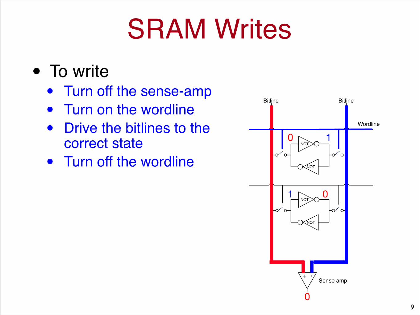
1 0
SRAM Writes• To write• Turn off the sense-amp• Turn on the wordline• Drive the bitlines to the
correct state• Turn off the wordline
NOT
NOT
Bitline Bitline
Wordline
NOT
NOT
-+
Sense amp
1 0
09
SRAM Writes• To write• Turn off the sense-amp• Turn on the wordline• Drive the bitlines to the
correct state• Turn off the wordline
NOT
NOT
Bitline Bitline
Wordline
NOT
NOT
-+
Sense amp
1 0
0
10
9

SRAM Writes• To write• Turn off the sense-amp• Turn on the wordline• Drive the bitlines to the
correct state• Turn off the wordline
NOT
NOT
Bitline Bitline
Wordline
NOT
NOT
-+
Sense amp
1 0
0
10
9
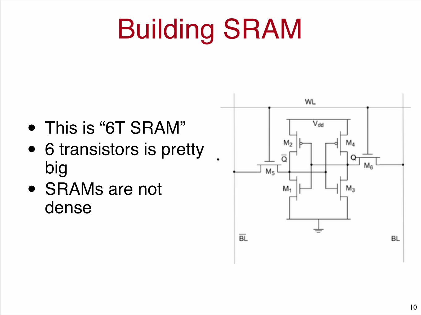
Building SRAM
• This is “6T SRAM”• 6 transistors is pretty
big• SRAMs are not
dense
10
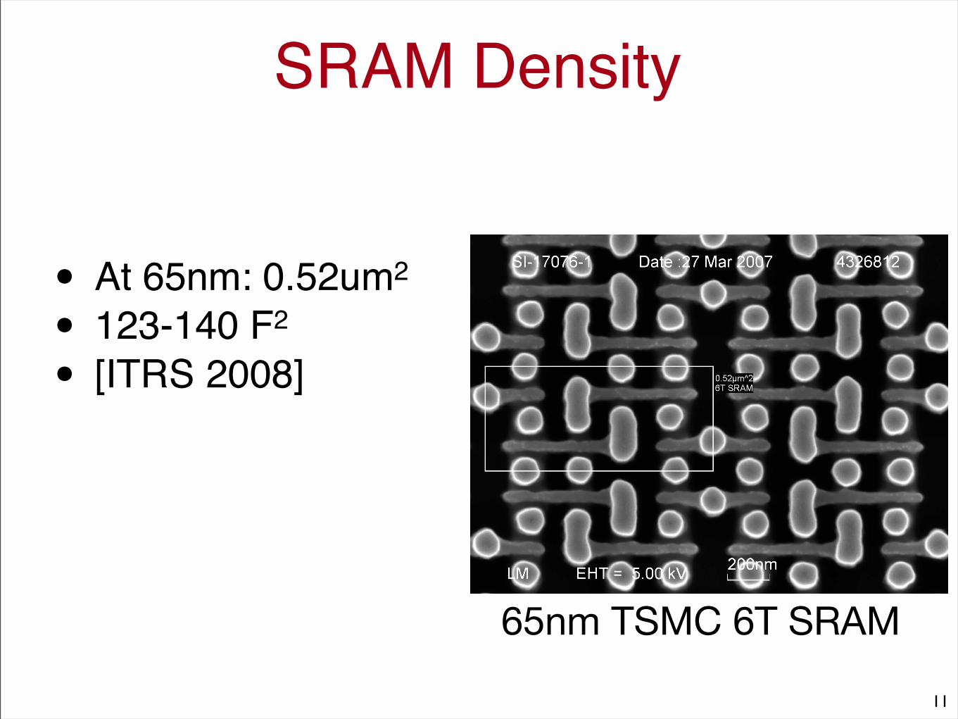
SRAM Density
• At 65nm: 0.52um2
• 123-140 F2
• [ITRS 2008]
65nm TSMC 6T SRAM
11
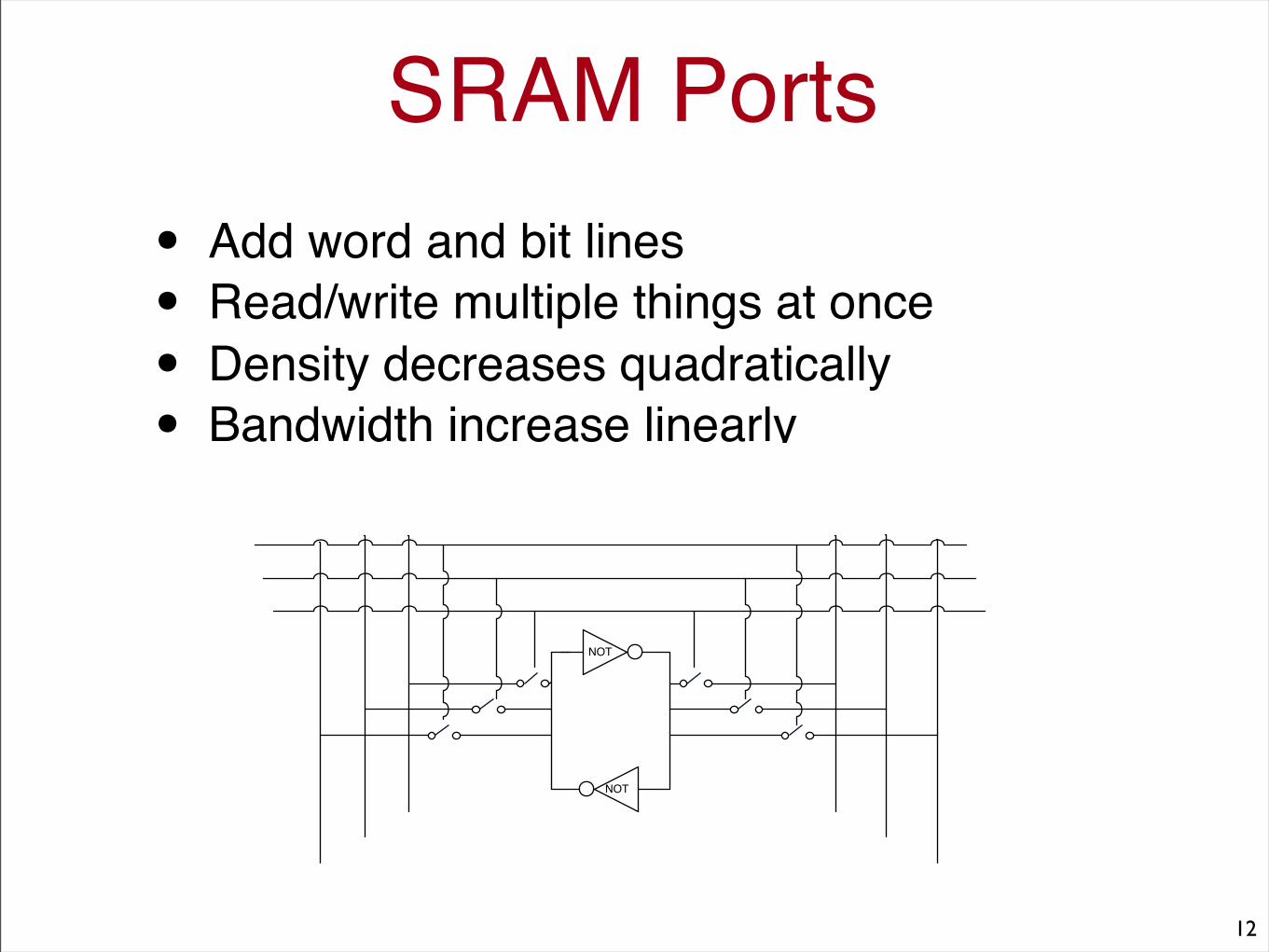
SRAM Ports• Add word and bit lines• Read/write multiple things at once• Density decreases quadratically• Bandwidth increase linearly
NOT
NOT
12

SRAM Performance• Read and write times• 10s-100s of ps• Bandwidth• Registers -- 324GB/s• L1 cache -- 128GB/s•
13
SRAM’s future• SRAM is a mature technology. No new, big
breakthroughs or advances are expected beyond CMOS scaling.
14


