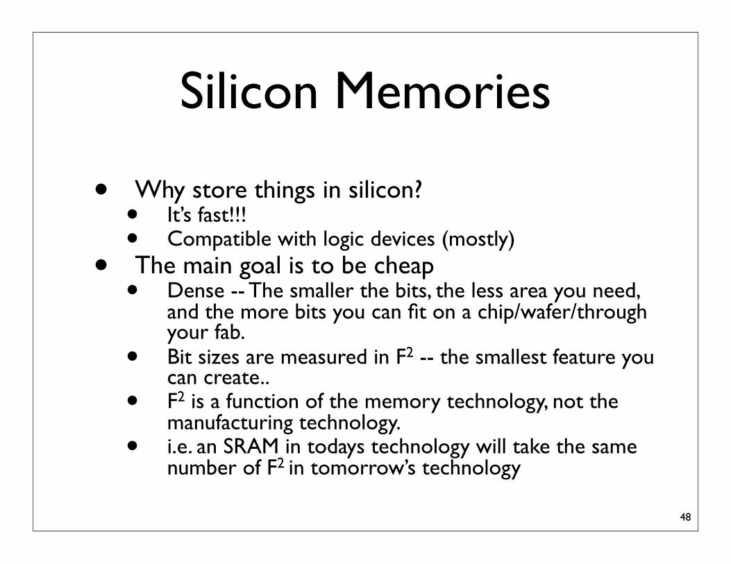
Silicon Memories • Why store things in silicon? • It’s fast!!! • Compatible with logic devices (mostly) • The main goal is to be cheap • Dense -- The smaller the bits, the less area you need, and the more bits you can fit on a chip/wafer/through your fab. • Bit sizes are measured in F 2 -- the smallest feature you can create.. • F 2 is a function of the memory technology, not the manufacturing technology. • i.e. an SRAM in todays technology will take the same number of F 2 in tomorrow’s technology 48
Transcript
Silicon Memories
• Why store things in silicon?• It’s fast!!!• Compatible with logic devices (mostly)
• The main goal is to be cheap• Dense -- The smaller the bits, the less area you need,
and the more bits you can fit on a chip/wafer/through your fab.
• Bit sizes are measured in F2 -- the smallest feature you can create..
• F2 is a function of the memory technology, not the manufacturing technology.
• i.e. an SRAM in todays technology will take the same number of F2 in tomorrow’s technology
48
Questions
• What physical quantity should represent the bit?• Voltage/charge -- SRAMs, DRAMs, Flash memories• Magnetic orientation -- MRAMs• Crystal structure -- phase change memories• The orientation of organic molecules -- various exotic
technologies• All that’s required is that we can sense it and turn it
into a logic one or zero.
• How do we achieve maximum density?• How do we make them fast?
49
Anatomy of a Memory• Dense: Build a big
array• bigger the better• less other stuff• Bigger -> slower
• Row decoder• Select the row by
raising a “word line”
• Column decoder• Select a slice of the
row
• Decoders are pretty big.
50
Row
decoder
Column decoder
Sense Amps
High order bits
Low order bits
Storage array
DataAddress
The Storage Array
• Density is king.• Highly engineered, carefully tuned, automatically
generated.• The smaller the devices, the better.
• Making them big makes them slow.• Bit/word lines are long (millimeters)• They have large capacitance, so their RC delay is long• For the row decoder, use large transistors to drive
them hard. • For the bit cells...
• There are lots of these, so they need to be as small as possible (but not smaller)
51
Sense Amps
• Sense amplifiers take a difference between two signals and amplify it
• Two scenarios• Inputs are initially equal (“precharged”) -- they each
move in opposite directions• One input is a reference -- so only one signal moves
• Frequently used in memories• Sense amps can detect small analog signals from the
storage cell, and convert it into a logic one or logic zero.
52
Static Random Access Memory (SRAM)
• Storage• Voltage on a pair of cross-
coupled inverters• Durable in presence of
power
• To read• Pre-charge two bit lines to
Vcc/2• Turn on the “word line”• Read the output of the
sense-amp
1 0NOT
NOT
Bitline Bitline
Wordline
NOT
NOT
-+
Sense amp
1 0
153
1 0
SRAM Writes
• To write• Turn off the sense-
amp• Turn on the
wordline• Drive the bitlines
to the correct state• Turn off the
wordline
NOT
NOT
Bitline Bitline
Wordline
NOT
NOT
-+
Sense amp
1 0
0
10
54
Building SRAM
• This is “6T SRAM”• 6 “basic devices” is
pretty big• SRAMs are not
dense
55
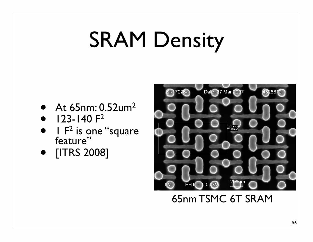
SRAM Density
• At 65nm: 0.52um2
• 123-140 F2
• 1 F2 is one “square feature”
• [ITRS 2008]
65nm TSMC 6T SRAM
56
SRAM Ports
• Add word and bit lines• Read/write multiple things at once• Density decreases quadratically• Bandwidth increase linearly
• Data clocked on rising and falling edge of the clock.
• DDR2• DDR3• GDDR2-5 -- For graphics cards.
DDR3 SDRAM
• DIMM data path is 64bits (72 with ECC)• Data rate: up to 1066Mhz
DDR (2133Mhz effective)• Bandwidth per DIMM GTNE:
16GB/s• guaranteed not to exceed
• Multiple DIMMs can attach to a bus• Reduces bandwidth/GB (a good idea?)
Each chip provides one 8-bit slice.
The chips are all synchronized and received
the same commands
Power
• DRAM is a major power sink.• Idle power: 2-4W/
DIMM• Active power: 5-8W/
DIMM
Economou, et. al 2006
DRAM Scaling
• Long term need for performance has driven DRAM hard• complex interface.• High performance• High power.
• DRAM used to be the main driver for process scaling, now it’s flash.
• Power is now a major concern.• Scaling is expected to match CMOS tech scaling• F2 cell size will probably not decrease• Historical foot note: Intel got its start as a DRAM company, but
got out of it when it became a commodity.
Technology Scaling
71
Moore’s Law: 2X transistors / “year”
“Cramming More Components onto Integrated Circuits”– Gordon Moore, Electronics, 1965
The essence of Moore’s Law: scale each dimension by ~1/√2 = ~0.71
180 nm 130 nm 90 nm
18.2 mm
× .72 = 13.1 mm
× .69 =9.04 mm
“Process” or “Lithography” or “Litho” Generationsmallest wire pitch = ~ 2-3x litho
each scaling halves the area of a fixed design
New Design
180 130 90
65 45
nm
Shrink Shrink
New Design
ShrinkShrink
order of release
The same design is oftenshrunk through multipleprocess generationsbefore coming up with a new micro-architecture,which is adjusted fortechnology changes.
New Design
180 130 90
65 45
order of releasenm
Shrink Shrink
New Design
ShrinkShrink
“Too big”
“Just Right”
“Debug new process; handoff”
Because chip costs scalewith around the square of die size, there is a “target die size” …
More on Scaling
• Seminal paper on scaling is Dennard et. al. “Design of ion-implanted MOSFET's with very small physical dimensions”, 1974
• Lays out how to build truly scalable transistors.
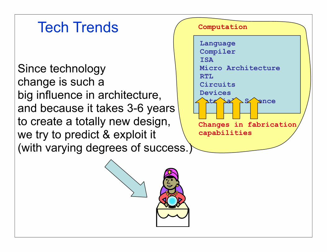
Tech Trends Language Compiler ISAMicro ArchitectureRTLCircuitsDevicesMaterials Science
Changes in fabrication capabilities
Computation
Since technologychange is such abig influence in architecture,and because it takes 3-6 yearsto create a totally new design, we try to predict & exploit it (with varying degrees of success.)
the power wall - has reduced abilityof these things tofurther improve frequency
• Moore’s Law is a conspiracy Webster conspiracy: - 2 : to act in harmony toward a common end
The chip (semiconductor) industry consists of many players – equipment manufacturers (e.g. lithography, mask making equipment), chip makers, computer aided design (CAD) companies, and end-sellers. It more or less runs in lock step. No one company can go too far ahead in process generations without the others.
In fact – they all plan together what to shoot for according to a schedule over the next 15 years!
Final Thoughts on Moore’s Law
International Technology Roadmap for Semiconductors (ITRS)http://www.itrs.net/
Future Target
Current
Red: we have no ideaYellow: some research will get us there