23
Microelectronic Packaging: The Rough of It Will Stoll Advisor: Dr. Fuhan Liu OR Improvement of Adhesion between Dielectric and Seed Layer for Next Generation System-on-Package (SOP)
| Date post: | 03-Aug-2018 |
| Category: |
Documents |
| Upload: | hoangkhanh |
| View: | 217 times |
| Download: | 0 times |
Microelectronic Packaging: The Rough of It
Will Stoll
Advisor: Dr. Fuhan Liu
OR
Improvement of Adhesion between Dielectric and Seed Layer for Next Generation System-on-Package (SOP)

Microelectronic Packaging
Moore’s Law exponential rise
in performance coupled with an exponential drop in price
integrated circuit innovations

Microelectronic Packaging
Packaging Printed Circuit Boards
– Multiple paths to individual components
System-On-A-Package (SOP)
– Embedded electronic components in a high density multilayered substrate
http://www.dorsetforyou.com/media/images/e/t/CompletedPrintedCircuitBoard.jpg
ULTRA HIGH DENSITY I/O INTERFACE • RF • OPTICAL • ELECTRICAL
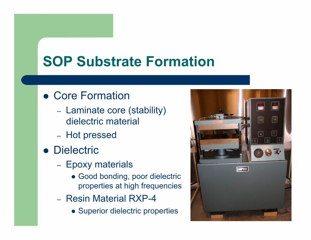
SOP Substrate Formation
Core Formation – Laminate core (stability)
dielectric material – Hot pressed
Dielectric – Epoxy materials
Good bonding, poor dielectric properties at high frequencies
– Resin Material RXP-4 Superior dielectric properties

SOP Substrate Formation
Photolithography – transfer images with UV light
onto photosensitive material (photo resist)
– Lamination of photoresist – Photolithography – Development
Laminate
Photolithography – exposure
Development

Metallization – Subtractive Etching
Laminate
Photolithography – exposure
Photolithography – development
Etching and Stripping of Photoresist

Metallization – Subadditive Etching
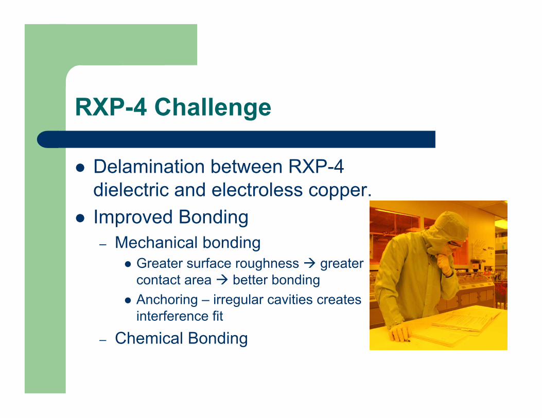
RXP-4 Challenge
Delamination between RXP-4 dielectric and electroless copper.
Improved Bonding – Mechanical bonding
Greater surface roughness greater contact area better bonding
Anchoring – irregular cavities creates interference fit
– Chemical Bonding
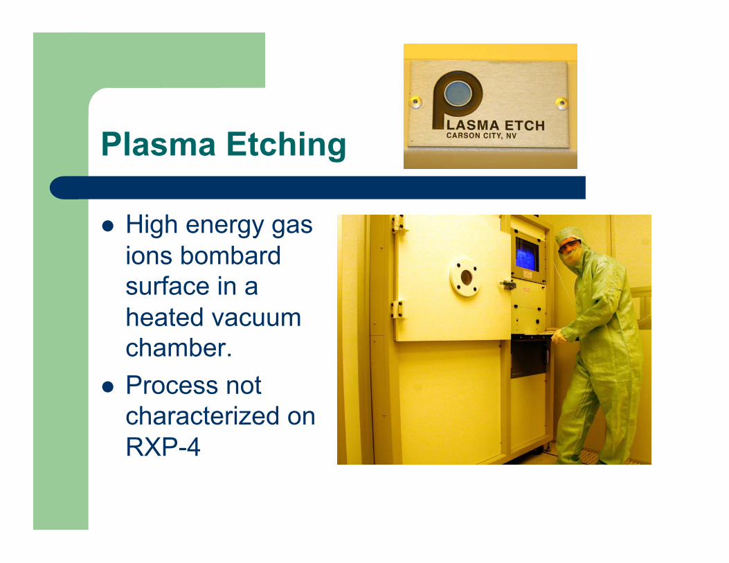
Plasma Etching
High energy gas ions bombard surface in a heated vacuum chamber.
Process not characterized on RXP-4
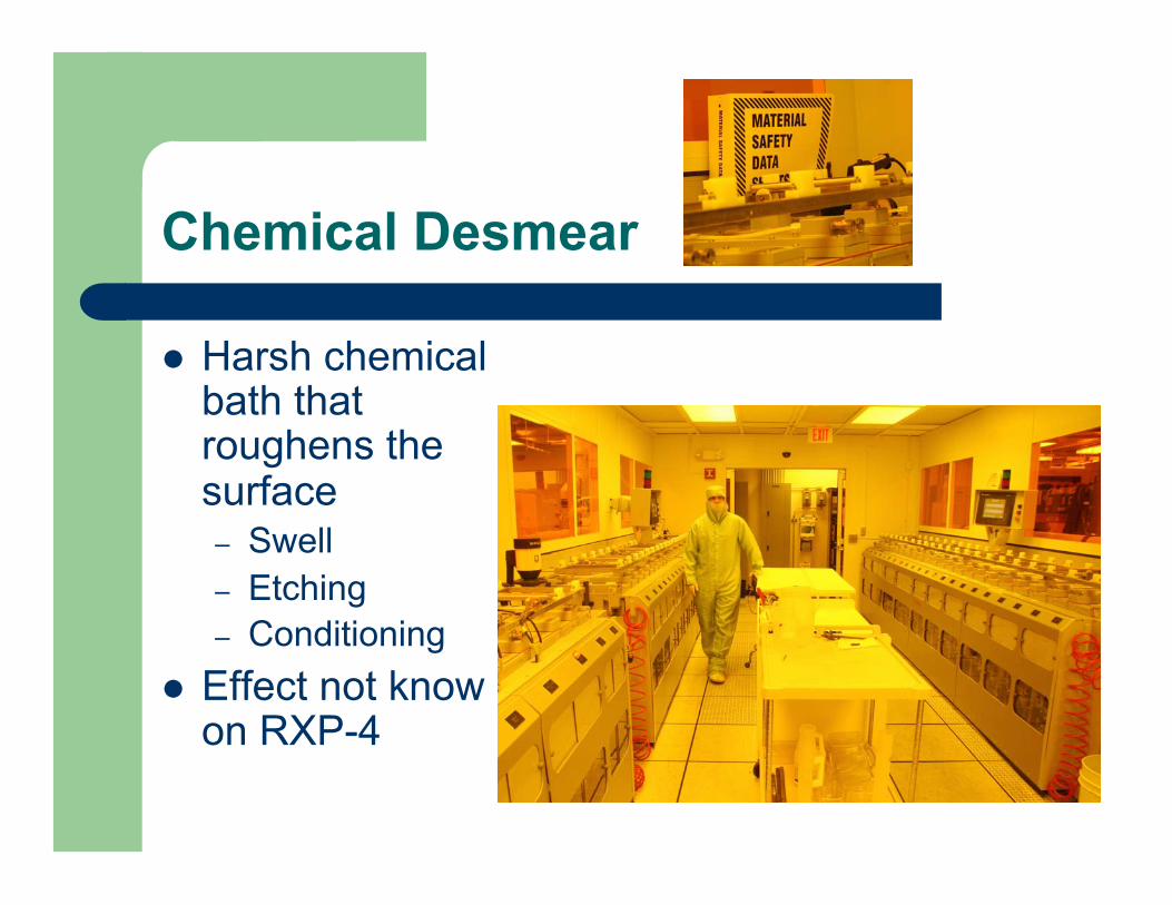
Chemical Desmear
Harsh chemical bath that roughens the surface – Swell – Etching – Conditioning
Effect not know on RXP-4

Experimental Work
Increase the surface roughness of RXP-4 Plasma Etching
– Gas Flow Rate – Gas Composition – Gas Time Exposure
Chemical Desmear – Swell and Etching Times

Surface Roughness Measurements
DekTak 3030 Surface Profiler Measuring System. Diamond-tipped stylus Measures the surface
electromechanically

RXP-4 Samples
Plasma Treated Untreated
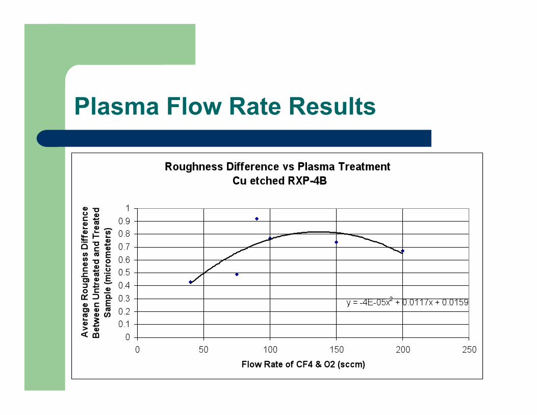
Plasma Flow Rate Results

Plasma Gas Composition Results

Plasma Gas Time Exposure Results

Plasma Gas Time Exposure Results
Time Average Roughness Difference
(µm) ±0.2µm Etched Thickness
(minutes) Plasma-Prior Plasma-Glass (µm)±1µm
20 0.73 0.83 12.44
15 0.64 0.7 8.72
12 0.21 0.27 3.52
10 0.6 0.49 2.8
8 0.23 0.22 N/A
5 0.07 0.22 2.23

Chemical Desmearing Results
Sample Time (minutes) Before Plasma Difference
Swell Etching µm µm µm R1 5 10 0.51 0.58 0.07 R2 10 20 0.48 0.47 -0.01 R3 15 30 0.46 0.55 0.09 R0 0 0 0.47 GT1 5 10 0.36 GT2 10 20 0.36 GT3 30 30 0.57

Chemical Desmearing Results

Conclusions
Plasma Etching increased surface roughness or RXP-4 consistently to 1µm. – Optimal parameters (100 C, 400 W Rf Power)
100/25 cc/min 02/CF4 flow rate 10-15 minutes
No increase in surface roughness with Chemical Desmear
Final conclusion awaiting industry adhesion test results

Research Link to Classroom
Great stories (real-life research examples) Professional contacts
Lesson Plan & Modern Physics Education
New cafeteria worker? Future Intel
commercial star?
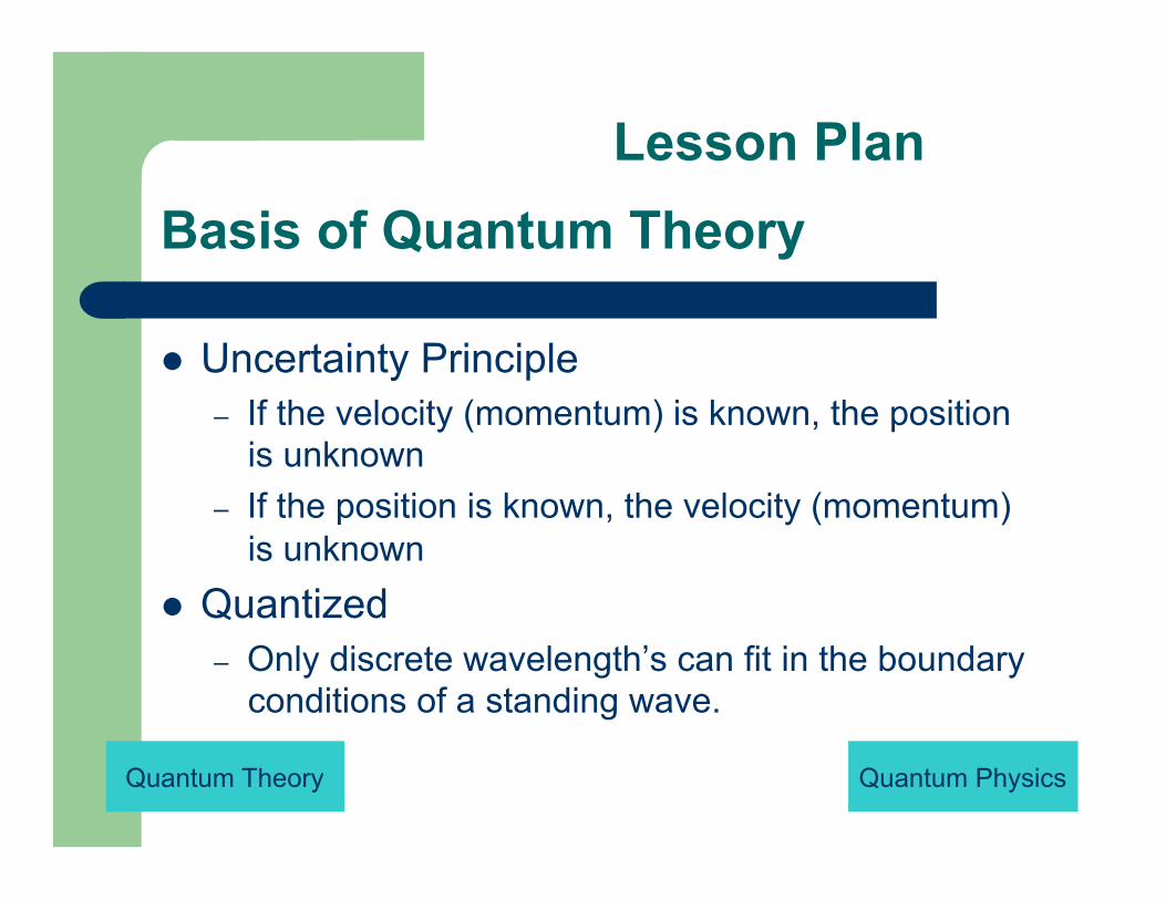
Basis of Quantum Theory
Uncertainty Principle – If the velocity (momentum) is known, the position
is unknown – If the position is known, the velocity (momentum)
is unknown Quantized
– Only discrete wavelength’s can fit in the boundary conditions of a standing wave.
Quantum Physics Quantum Theory
Lesson Plan
Acknowledgements
Direction Dr Fuhan Liu and Dr Venky Sundaram Support Ganesh Krishnan, Boon Teong Lee, Hunter
Chan, Jason Bishop, Mike Toole Vision Dr. Leyla Conrad and Dr. Ed Conrad Resources NSF and PRC


