8
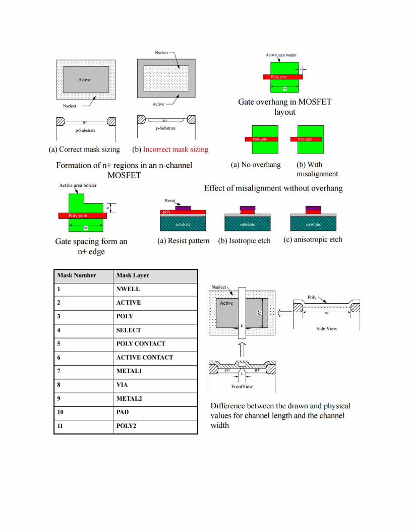
There are two types of MOS transistors. They are called n-channel MOS transistor (NMOS) and p-channel MOS transistor (PMOS). Each transistor has 4 terminals, namely drain (D), gate (G), source (S) and bulk (B) as illustrated in the transistor symbols. The bulks of the PMOS and the NMOS are usually connected to power and ground respectively. If the bulk terminal is omitted from the schematic symbol, the connections can be assumed to be what is shown in the following diagram. A circuit design usually uses more than one type of PMOS or NMOS to cater for different power supply voltages. For example, a design may use thicker gate-oxide transistors to operate in higher power supply at the I/O interfaces. In order to differentiate the various voltage range transistors, sometimes circuit designers conveniently make use of the “depletion-mode” transistor symbol for this purpose. Typically, the schematic symbols for the depletion-mode transistors are represented with a thicker gate drawing The MOS transistor’s performance varies with its channel length (L) and channel width (W). The drain current (ID) that flows through the transistor operating in the saturation mode is shown in the following equation. where K and λ can be taken as process technology constants. Note that ID is proportional to the ratio of W over L. Typically L is kept to the minimum dimension allowed in the design rule, and is to be layout exactly as indicated in the schematic. However, this is not always the case for W. Physical structure of ICs - `Design rules `Basic gates layout