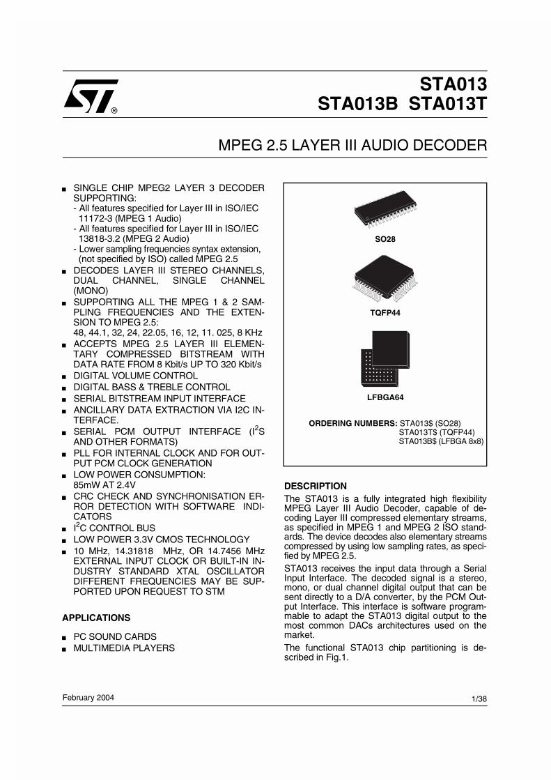
February 2004 ORDERING NUMBERS: STA013$ (SO28) STA013T$ (TQFP44) STA013B$ (LFBGA 8x8) SINGLE CHIP MPEG2 LAYER 3 DECODER SUPPORTING: - All features specified for Layer III in ISO/IEC 11172-3 (MPEG 1 Audio) - All features specified for Layer III in ISO/IEC 13818-3.2 (MPEG 2 Audio) - Lower sampling frequencies syntax extension, (not specified by ISO) called MPEG 2.5 DECODES LAYER III STEREO CHANNELS, DUAL CHANNEL, SINGLE CHANNEL (MONO) SUPPORTING ALL THE MPEG 1 & 2 SAM- PLING FREQUENCIES AND THE EXTEN- SION TO MPEG 2.5: 48, 44.1, 32, 24, 22.05, 16, 12, 11. 025, 8 KHz ACCEPTS MPEG 2.5 LAYER III ELEMEN- TARY COMPRESSED BITSTREAM WITH DATA RATE FROM 8 Kbit/s UP TO 320 Kbit/s DIGITAL VOLUME CONTROL DIGITAL BASS & TREBLE CONTROL SERIAL BITSTREAM INPUT INTERFACE ANCILLARY DATA EXTRACTION VIA I2C IN- TERFACE. SERIAL PCM OUTPUT INTERFACE (I 2 S AND OTHER FORMATS) PLL FOR INTERNAL CLOCK AND FOR OUT- PUT PCM CLOCK GENERATION LOW POWER CONSUMPTION: 85mW AT 2.4V CRC CHECK AND SYNCHRONISATION ER- ROR DETECTION WITH SOFTWARE INDI- CATORS I 2 C CONTROL BUS LOW POWER 3.3V CMOS TECHNOLOGY 10 MHz, 14.31818 MHz, OR 14.7456 MHz EXTERNAL INPUT CLOCK OR BUILT-IN IN- DUSTRY STANDARD XTAL OSCILLATOR DIFFERENT FREQUENCIES MAY BE SUP- PORTED UPON REQUEST TO STM APPLICATIONS PC SOUND CARDS MULTIMEDIA PLAYERS DESCRIPTION The STA013 is a fully integrated high flexibility MPEG Layer III Audio Decoder, capable of de- coding Layer III compressed elementary streams, as specified in MPEG 1 and MPEG 2 ISO stand- ards. The device decodes also elementary streams compressed by using low sampling rates, as speci- fied by MPEG 2.5. STA013 receives the input data through a Serial Input Interface. The decoded signal is a stereo, mono, or dual channel digital output that can be sent directly to a D/A converter, by the PCM Out- put Interface. This interface is software program- mable to adapt the STA013 digital output to the most common DACs architectures used on the market. The functional STA013 chip partitioning is de- scribed in Fig.1. STA013 STA013B STA013T MPEG 2.5 LAYER III AUDIO DECODER ® SO28 TQFP44 LFBGA64 1/38
SINGLE CHIP MPEG2 LAYER 3 DECODERSUPPORTING:- All features specified for Layer III in ISO/IEC 11172-3 (MPEG 1 Audio)- All features specified for Layer III in ISO/IEC 13818-3.2 (MPEG 2 Audio)- Lower sampling frequencies syntax extension, (not specified by ISO) called MPEG 2.5DECODES LAYER III STEREO CHANNELS,DUAL CHANNEL, SINGLE CHANNEL(MONO)SUPPORTING ALL THE MPEG 1 & 2 SAM-PLING FREQUENCIES AND THE EXTEN-SION TO MPEG 2.5:48, 44.1, 32, 24, 22.05, 16, 12, 11. 025, 8 KHzACCEPTS MPEG 2.5 LAYER III ELEMEN-TARY COMPRESSED BITSTREAM WITHDATA RATE FROM 8 Kbit/s UP TO 320 Kbit/sDIGITAL VOLUME CONTROLDIGITAL BASS & TREBLE CONTROLSERIAL BITSTREAM INPUT INTERFACEANCILLARY DATA EXTRACTION VIA I2C IN-TERFACE.SERIAL PCM OUTPUT INTERFACE (I2SAND OTHER FORMATS)PLL FOR INTERNAL CLOCK AND FOR OUT-PUT PCM CLOCK GENERATIONLOW POWER CONSUMPTION:85mW AT 2.4VCRC CHECK AND SYNCHRONISATION ER-ROR DETECTION WITH SOFTWARE INDI-CATORSI2C CONTROL BUSLOW POWER 3.3V CMOS TECHNOLOGY10 MHz, 14.31818 MHz, OR 14.7456 MHzEXTERNAL INPUT CLOCK OR BUILT-IN IN-DUSTRY STANDARD XTAL OSCILLATORDIFFERENT FREQUENCIES MAY BE SUP-PORTED UPON REQUEST TO STM
APPLICATIONS
PC SOUND CARDSMULTIMEDIA PLAYERS
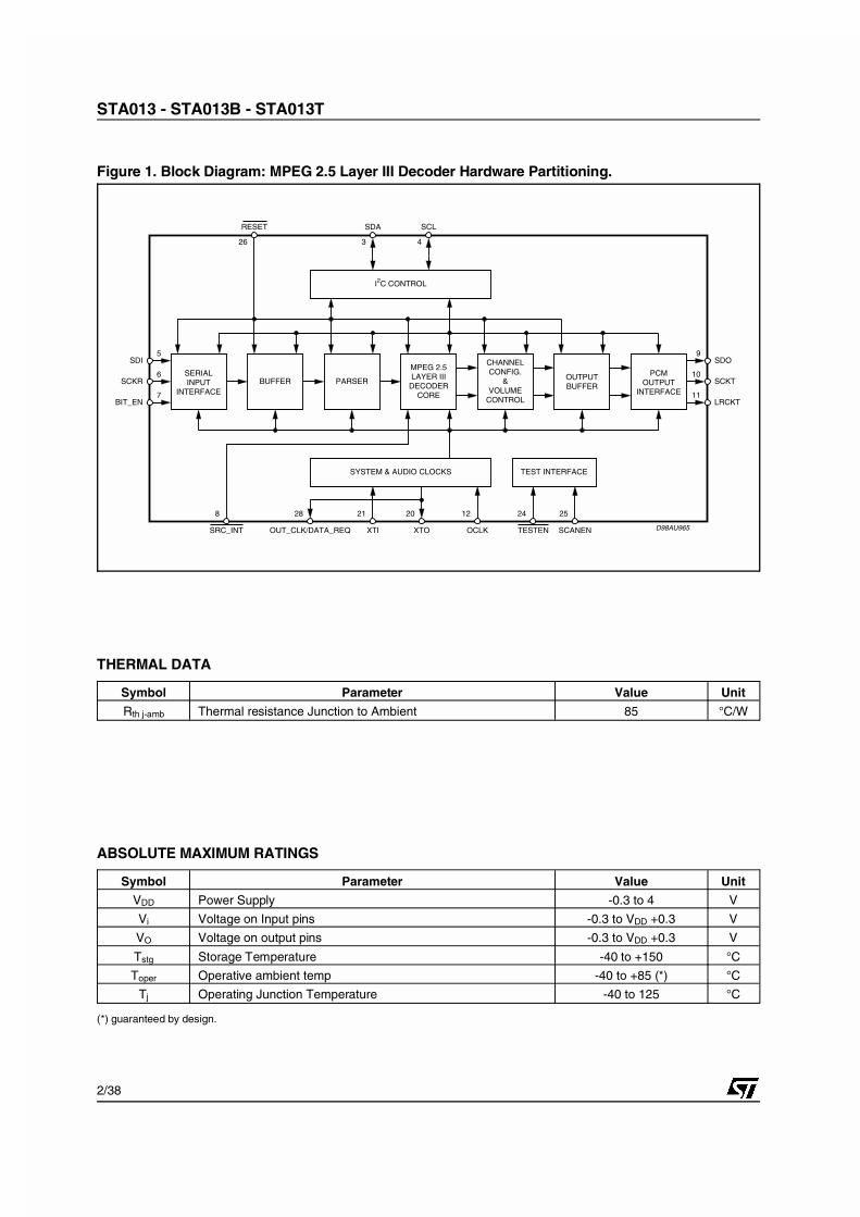
DESCRIPTIONThe STA013 is a fully integrated high flexibilityMPEG Layer III Audio Decoder, capable of de-coding Layer III compressed elementary streams,as specified in MPEG 1 and MPEG 2 ISO stand-ards. The device decodes also elementary streamscompressed by using low sampling rates, as speci-fied by MPEG 2.5.STA013 receives the input data through a SerialInput Interface. The decoded signal is a stereo,mono, or dual channel digital output that can besent directly to a D/A converter, by the PCM Out-put Interface. This interface is software program-mable to adapt the STA013 digital output to themost common DACs architectures used on themarket.The functional STA013 chip partitioning is de-scribed in Fig.1.
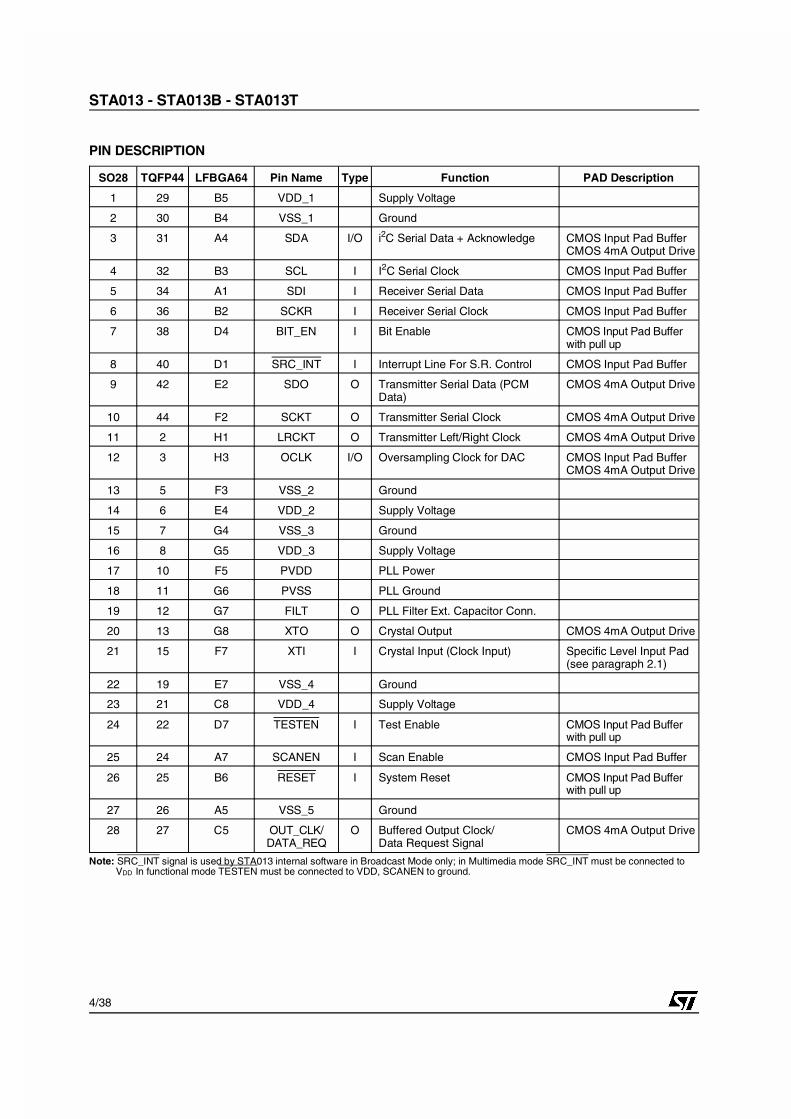
21 15 F7 XTI I Crystal Input (Clock Input) Specific Level Input Pad(see paragraph 2.1)
22 19 E7 VSS_4 Ground
23 21 C8 VDD_4 Supply Voltage
24 22 D7 TESTEN I Test Enable CMOS Input Pad Bufferwith pull up
25 24 A7 SCANEN I Scan Enable CMOS Input Pad Buffer
26 25 B6 RESET I System Reset CMOS Input Pad Bufferwith pull up
27 26 A5 VSS_5 Ground
28 27 C5 OUT_CLK/DATA_REQ
O Buffered Output Clock/Data Request Signal
CMOS 4mA Output Drive
Note: SRC_INT signal is used by STA013 internal software in Broadcast Mode only; in Multimedia mode SRC_INT must be connected to VDD In functional mode TESTEN must be connected to VDD, SCANEN to ground.
Symbol Parameter Test Condition Min. Typ. Max. Unit Note
IIL Low Level Input CurrentWithout pull-up device
Vi = 0V -10 10 µA 1
IIH High Level Input CurrentWithout pull-up device
Vi = VDD = 3.6V -10 10 µA 1
Vesd Electrostatic Protection Leakage < 1µA 2000 V 2
Note 1: The leakage currents are generally very small, < 1nA. The value given here is a maximum that can occur after an electrostatic stresson the pin.Note 2: Human Body Model.
DC ELECTRICAL CHARACTERISTICS
Symbol Parameter Test Condition Min. Typ. Max. Unit Note
VIL Low Level Input Voltage 0.2*VDD V
VIH High Level Input Voltage 0.8*VDD V
Vol Low Level Output Voltage Iol = Xma 0.4V V 1, 2
Voh High Level Output Voltage 0.85*VDD V 1, 2
Note 1: Takes into account 200mV voltage drop in both supply lines.Note 2: X is the source/sink current under worst case conditions and is reflected in the name of the I/O cell according to the drive capability.
Symbol Parameter Test Condition Min. Typ. Max. Unit Note
Ipu Pull-up current Vi = 0V; pin numbers 7, 24and 26; VDD = 3V
-25 -66 -125 µA 1
Rpu Equivalent Pull-upResistance
50 kΩ
Note 1: Min. condition: VDD = 2.4V, 125°C Min process Max. condition: VDD = 3.6V, -20°C Max.
POWER DISSIPATION
Symbol Parameter Test Condition Min. Typ. Max. Unit Note
PD Power Dissipation@ VDD = 3V
Sampling_freq ≤24 kHz 76 mW
Sampling_freq ≤32 kHz 79 mW
Sampling_freq ≤48 kHz 85 mW
STA013 - STA013B - STA013T
5/38
VDD
100nF
1
2
VDD
100nF
14
13
VSS
VDD
100nF
16
15
VDD
100nF
23
22
VSS
VSS
VSS17 18 27
28
26
RESET
24
TESTEN
25
SCANEN
OUT_CLK/DATA_REQ
VDD
PVSSPVDD
100nF
4.7µF 4.7µF
PVDD
PVSSVSS
10K
1K
4.7nF
PVSS
470pF
19
20
21
8
7
6
5
12
11
10
9
4
3
XTO
XTI
SCR_INT
BIT_EN
SCKR
SDI
OCLK
LRCKT
SCKT
SDO
SCL
SDA
D98AU966
Figure 3. Test Circuit
IOL
IOHCL
VREF
VDD
OUTPUT
D98AU967
Figure 4. Test Load Circuit
Output IOL IOH CL VREF
SDA 1mA 100pF 3.6V
Other Outputs 100µA 100µA 100pF 1.5V
Test Load
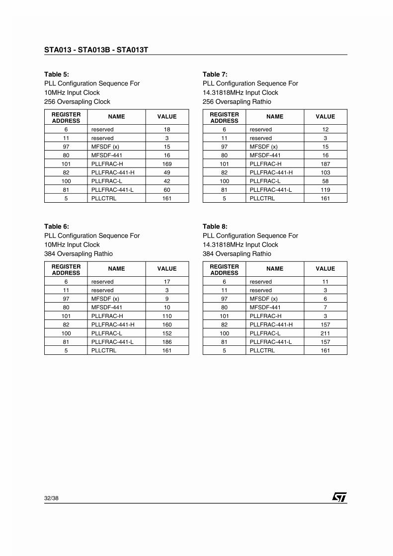
2. FUNCTIONAL DESCRIPTION2.1 - Clock SignalThe STA013 input clock is derivated from an ex-ternal source or from a industry standard crystaloscillator, generating input frequencies of 10,14.31818 or 14.7456 MHz.
Other frequencies may be supported upon re-quest to STMicroelectronics. Each frequency issupported by downloading a specific configura-tion file, provided by STMXTI is an input Pad with specific levels.
Symbol Parameter Test Condition Min. Typ. Max. Unit
VIL Low Level Input Voltage VDD-1.8 V
VIH High Level Input Voltage VDD-0.8 V
CMOS compatibilityThe XTI pad low and high levels are CMOS compatible; XTI pad noise margin is better than typicalCMOS pads.TTL compatibilityThe XTI pad low level is compatible with TTL while the high level is not compatible (for example if VDD =3V TTL min high level = 2.0V while XTI min high level = 2.2V)
STA013 - STA013B - STA013T
6/38
SCLK_POL=0
SCLK_POL=4
DATA IGNOREDDATA VALID
SCKR
SCKR
SDI
BIT_END98AU968A
DATA IGNORED
Figure 6. Serial Input Interface Clocks
DATASOURCE
µP
MPEGDECODER
IIC
D98AU912
IIC
SDO
SCKT
LRCKT
SERIAL AUDIO INTERFACE
SDI
SCKR
BIT_EN
XTO
DAC
RX TX
XTI FILT
PLL
OCLK
SCL SDA
DATA_REQ
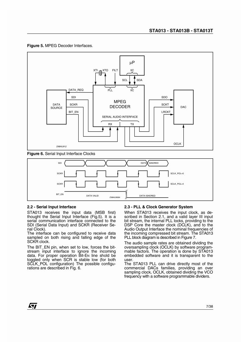
Figure 5. MPEG Decoder Interfaces.
2.2 - Serial Input InterfaceSTA013 receives the input data (MSB first)thought the Serial Input Interface (Fig.5). It is aserial communication interface connected to theSDI (Serial Data Input) and SCKR (Receiver Se-rial Clock).The interface can be configured to receive datasampled on both rising and falling edge of theSCKR clock.The BIT_EN pin, when set to low, forces the bit-stream input interface to ignore the incomingdata. For proper operation Bit-EN line shold betoggled only when SCR is stable low (for bothSCLK_POL configuration) The possible configu-rations are described in Fig. 6.
2.3 - PLL & Clock Generator SystemWhen STA013 receives the input clock, as de-scribed in Section 2.1, and a valid layer III inputbit stream, the internal PLL locks, providing to theDSP Core the master clock (DCLK), and to theAudio Output Interface the nominal frequencies ofthe incoming compressed bit stream. The STA013PLL block diagram is described in Figure 7.The audio sample rates are obtained dividing theoversampling clock (OCLK) by software program-mable factors. The operation is done by STA013embedded software and it is transparent to theuser. The STA013 PLL can drive directly most of thecommercial DACs families, providing an oversampling clock, OCLK, obtained dividing the VCOfrequency with a software programmable dividers.
STA013 - STA013B - STA013T
7/38
R
CC
XTI2DSPCLK
XTI2OCLK
X
S
N
M
PFD CP
VCO
SwitchingCircuit
OCLK
DCLKUpdate FRAC
FRAC
XTI
Disable PLL
Figure 7. PLL and Clocks Generation System
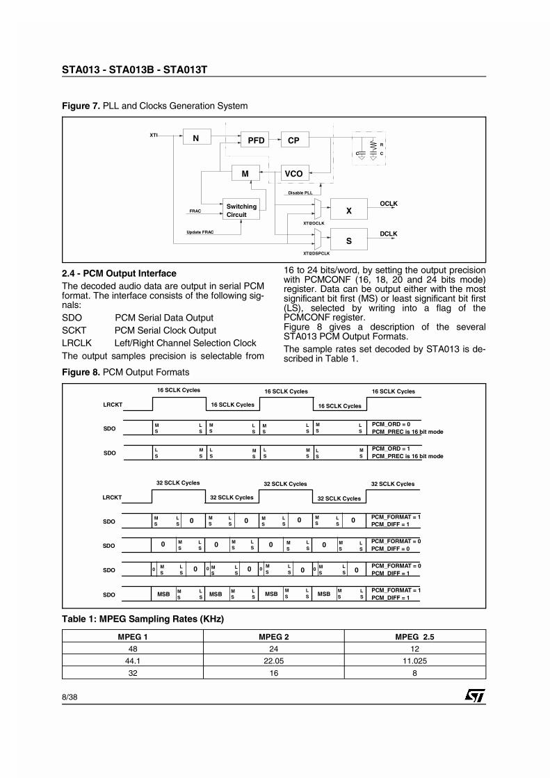
2.4 - PCM Output InterfaceThe decoded audio data are output in serial PCMformat. The interface consists of the following sig-nals:SDO PCM Serial Data OutputSCKT PCM Serial Clock OutputLRCLK Left/Right Channel Selection ClockThe output samples precision is selectable from
16 to 24 bits/word, by setting the output precisionwith PCMCONF (16, 18, 20 and 24 bits mode)register. Data can be output either with the mostsignificant bit first (MS) or least significant bit first(LS), selected by writing into a flag of thePCMCONF register.Figure 8 gives a description of the severalSTA013 PCM Output Formats.The sample rates set decoded by STA013 is de-scribed in Table 1.
LRCKT
SDO
SDOPCM_FORMAT = 0 PCM_DIFF = 0
PCM_FORMAT = 1 PCM_DIFF = 1
32 SCLK Cycles
32 SCLK Cycles32 SCLK Cycles 32 SCLK Cycles
32 SCLK Cycles
MS
MS
LS
LS
LS
LS
MS
MS
MS
LS
MS
LS
LS
LS
MS
MS
LRCKT
SDO
SDOPCM_ORD = 1 PCM_PREC is 16 bit mode
PCM_ORD = 0 PCM_PREC is 16 bit mode
16 SCLK Cycles
16 SCLK Cycles16 SCLK Cycles 16 SCLK Cycles
16 SCLK Cycles
MS
MS
LS
LS
LS
LS
MS
MS
MS
LS
MS
LS
LS
LS
MS
MS
SDOPCM_FORMAT = 0PCM_DIFF = 1
LS
LS
MS
MS
MS
LS
LS
MS
SDOPCM_FORMAT = 1 PCM_DIFF = 1
LS
LS
MS
MS
MS
LS
LS
MS
0000
0000
0 0 0 00 0 0 0
MSBMSB MSB MSB
Figure 8. PCM Output Formats
Table 1: MPEG Sampling Rates (KHz)
MPEG 1 MPEG 2 MPEG 2.5
48 24 12
44.1 22.05 11.025
32 16 8
STA013 - STA013B - STA013T
8/38
2.5 - STA013 Operation ModeThe STA013 can work in two different modes,called Multimedia Mode and Broadcast Mode.In Multimedia Mode, STA013 decodes the in-coming bitstream, acting as a master of the datacommunication from the source to itself.This control is done by a specific buffer manage-ment, controlled by STA013 embedded software.The data source, by monitoring the DATA_REQline, send to STA013 the input data, when thesignal is high (default configuration).The communication is stopped when theDATA_REQ line is low.In this mode the fractional part of the PLL is dis-abled and the audio clocks are generated atnominal rates. Fig. 9 describes the defaultDATA_REQ signal behaviour.Programming STA013 it is possible to invert thepolarity of the DATA_REQ line (registerREQ_POL).
In Broadcast Mode, STA013 works receiving abitstream with the input speed regulated by thesource. In this configuration the source has toguarantee that the bitrate is equivalent to thenominal bitrate of the decoded stream.To compensate the difference between the nomi-nal and the real sampling rates, the STA013 em-bedded software controls the fractional PLL op-eration. Portable or Mobile applications neednormally to operate in Broadcast Mode. In bothmodes the MPEG Synchronisation is automaticand transparent to the user. To operate in Multi-media mode, the STA013, pin nr. 8, SCR-INTmust be connected to VDD on the applicationboard.
2.6 - STA013 Decoding StatesThere are three different decoder states: Idle,Init, and Decode. Commands to change the de-coding states are described in the STA013 I2Cregisters description.
Idle ModeIn this mode the decoder is waiting for the RUNcommand. This mode should be used to initialise
the configuration register of the device. The DACconnected to STA013 can be initialised duringthis mode (set MUTE to 1).
PLAY MUTE Clock State PCM Output
X 0 Not Running 0
X 1 Running 0
Init Mode"PLAY" and "MUTE" changes are ignored in thismode. The internal state of the decoder will beupdated only when the decoder changes from thestate "init" to the state "decode". The "init" phaseends when the first decoded samples are at theoutput stage of the device.
Decode ModeThis mode is completely described by the follow-ing table:
PLAY MUTE Clock State PCMOutput Decoding
0 0 Not Running 0 No
0 1 Running 0 No
1 0 Running DecodedSamples
Yes
1 1 Running 0 Yes
3 - I2C BUS SPECIFICATIONThe STA013 supports the I2C protocol. This pro-tocol defines any device that sends data on to thebus as a transmitter and any device that readsthe data as a receiver. The device that controlsthe data transfer is known as the master and theothers as the slave. The master always starts thetransfer and provides the serial clock for synchro-nisation. The STA013 is always a slave device inall its communications.
3. 1 - COMMUNICATION PROTOCOL
3.1.0 - Data transition or changeData changes on the SDA line must only occurwhen the SCL clock is low. SDA transition whilethe clock is high are used to identify START orSTOP condition.
3.1.1 - Start conditionSTART is identified by a high to low transition ofthe data bus SDA signal while the clock signalSCL is stable in the high state.A START condition must precede any commandfor data transfer.
SOURCE SEND DATA TO STA013
DATA_REQ
SOURCE STOPS TRANSMITTING DATA SOURCE STOPS TRANSMITTING DATA
D98AU913
Figure 9.
STA013 - STA013B - STA013T
9/38
3.1.2 - Stop conditionSTOP is identified by low to high transition of thedata bus SDA signal while the clock signal SCL isstable in the high state. A STOP condition termi-nates communications between STA013 and thebus master.
3.1.3 - Acknowledge bitAn acknowledge bit is used to indicate a success-ful data transfer. The bus transmitter, either mas-ter or slave, releases the SDA bus after sending8 bit of data.During the 9th clock pulse the receiver pulls theSDA bus low to acknowledge the receipt of 8 bitsof data.
3.1.4 - Data inputDuring the data input the STA013 samples theSDA signal on the rising edge of the clock SCL.For correct device operation the SDA signal hasto be stable during the rising edge of the clockand the data can change only when the SCL lineis low.
3.2 - DEVICE ADDRESSINGTo start communication between the master andthe STA013, the master must initiate with a startcondition. Following this, the master sends ontothe SDA line 8 bits (MSB first) corresponding tothe device select address and read or writemode.
The 7 most significant bits are the device addressidentifier, corresponding to the I2C bus definition.For the STA013 these are fixed as 1000011.The 8th bit (LSB) is the read or write operationRW, this bit is set to 1 in read mode and 0 forwrite mode. After a START condition the STA013identifies on the bus the device address and, if amatch is found, it acknowledges the identificationon SDA bus during the 9th bit time. The followingbyte after the device identification byte is the in-ternal space address.
3.3 - WRITE OPERATION (see fig. 10)Following a START condition the master sends adevice select code with the RW bit set to 0.The STA013 acknowledges this and waits for thebyte of internal address.After receiving the internal bytes address theSTA013 again responds with an acknowledge.
3.3.1 - Byte writeIn the byte write mode the master sends one databyte, this is acknowledged by STA013. The mas-ter then terminates the transfer by generating aSTOP condition.
3.3.2 - Multibyte writeThe multibyte write mode can start from any inter-nal address. The transfer is terminated by themaster generating a STOP condition.
DEV-ADDR
ACK
START
D98AU826A
RW
DATA
NO ACK
STOP
CURRENTADDRESS
READ
DEV-ADDR
ACK
START RW
SUB-ADDR
ACK
DEV-ADDR
ACK
STOP
RANDOMADDRESS
READ
DATA
NO ACK
START RW
DEV-ADDR
ACK
START
DATA
ACK
DATA
ACK
STOP
SEQUENTIALCURRENT
READ
DATA
NO ACK
DEV-ADDR
ACK
START RW
SUB-ADDR
ACK
DEV-ADDR
ACK
SEQUENTIALRANDOM
READ
DATA
ACK
START RW
DATA
ACK NO ACK
STOP
DATA
RW=HIGH
Figure 11. Read Mode Sequence
DEV-ADDR
ACK
START
D98AU825B
RW
SUB-ADDR
ACK
DATA IN
ACK
STOP
BYTEWRITE
DEV-ADDR
ACK
START RW
SUB-ADDR
ACK
DATA IN
ACK
STOP
MULTIBYTEWRITE
DATA IN
ACK
Figure 10. Write Mode Sequence
STA013 - STA013B - STA013T
10/38
3.4 - READ OPERATION (see Fig. 11)
3.4.1 - Current byte address readThe STA013 has an internal byte addresscounter. Each time a byte is written or read, thiscounter is incremented.For the current byte address read mode, follow-ing a START condition the master sends the de-vice address with the RW bit set to 1.The STA013 acknowledges this and outputs thebyte addressed by the internal byte addresscounter. The master does not acknowledge thereceived byte, but terminates the transfer with aSTOP condition.
3.4.2 - Sequential address readThis mode can be initiated with either a currentaddress read or a random address read. How-ever in this case the master does acknowledgethe data byte output and the STA013 continues tooutput the next byte in sequence.To terminate the streams of bytes the masterdoes not acknowledge the last received byte, but
terminates the transfer with a STOP condition.The output data stream is from consecutive byteaddresses, with the internal byte address counterautomatically incremented after one byte output.
4 - I2C REGISTERS The following table gives a description of theMPEG Source Decoder (STA013) register list. The first column (HEX_COD) is the hexadecimalcode for the sub-address.The second column (DEC_COD) is the decimalcode.The third column (DESCRIPTION) is the descrip-tion of the information contained in the register.The fourth column (RESET) inidicate the resetvalue if any. When no reset value is specifyed,the default is "undefined".The fifth column (R/W) is the flag to distinguishregister "read only" and "read and write", and theuseful size of the register itself.Each register is 8 bit wide. The master shall oper-ate reading or writing on 8 bits only.
I2C REGISTERS
HEX_COD DEC_COD DESCRIPTION RESET R/W
$00 0 VERSION R (8)
$01 1 IDENT 0xAC R (8)
$05 5 PLLCTL [7:0] 0xA1 R/W (8)
$06 6 PLLCTL [20:16] (MF[4:0]=M) 0x0C R/W (8)
$07 7 PLLCTL [15:12] (IDF[3:0]=N) 0x00 R/W (8)
$0B 11 reserved
$0C 12 REQ_POL 0x01 R/W (8)
$0D 13 SCLK_POL 0x04 R/W (8)
$0F 15 ERROR_CODE 0x00 R (8)
$10 16 SOFT_RESET 0x00 W (8)
$13 19 PLAY 0x01 R/W(8)
$14 20 MUTE 0x00 R/W(8)
$16 22 CMD_INTERRUPT 0x00 R/W(8)
$18 24 DATA_REQ_ENABLE 0x00 R/W(8)
$40 64 SYNCSTATUS 0x00 R (8)
$41 65 ANCCOUNT_L 0x00 R (8)
$42 66 ANCCOUNT_H 0x00 R (8)
STA013 - STA013B - STA013T
11/38
I2C REGISTERS (continued)
HEX_COD DEC_COD DESCRIPTION RESET R/W
$43 67 HEAD_H[23:16] 0x00 R(8)
$44 68 HEAD_M[15:8] 0x00 R(8)
$45 69 HEAD_L[7:0] 0x00 R(8)
$46 70 DLA 0x00 R/W (8)
$47 71 DLB 0xFF R/W (8)
$48 72 DRA 0x00 R/W (8)
$49 73 DRB 0xFF R/W (8)
$50 80 MFSDF_441 0x00 R/W (8)
$51 81 PLLFRAC_441_L 0x00 R/W (8)
$52 82 PLLFRAC_441_H 0x00 R/W (8)
$54 84 PCM DIVIDER 0x03 R/W (8)
$55 85 PCMCONF 0x21 R/W (8)
$56 86 PCMCROSS 0x00 R/W (8)
$59 89 ANC_DATA_1 [7:0] 0x00 R (8)
$5A 90 ANC_DATA_2 [15:8] 0x00 R (8)
$5B 91 ANC_DATA_3 [23:16] 0x00 R (8)
$5C 92 ANC_DATA_4 [31:24] 0x00 R (8)
$5D 93 ANC_DATA_5 [39:32] 0x00 R (8)
$61 97 MFSDF (X) 0x07 R/W (8)
$63 99 DAC_CLK_MODE 0x00 R/W (8)
$64 100 PLLFRAC_L 0x46 R/W (8)
$65 101 PLLFRAC_H 0x5B R/W (8)
$67 103 FRAME_CNT_L 0x00 R (8)
$68 104 FRAME_CNT_M 0x00 R (8)
$69 105 FRAME_CNT_H 0x00 R (8)
$6A 106 AVERAGE_BITRATE 0x00 R (8)
$71 113 SOFTVERSION R (8)
$72 114 RUN 0x00 R/W (8)
$77 119 TREBLE_FREQUENCY_LOW 0x00 R/W (8)
$78 120 TREBLE_FREQUENCY_HIGH 0x00 R/W (8)
$79 121 BASS_FREQUENCY_LOW 0x00 R/W (8)
$7A 122 BASS_FREQUENCY_HIGH 0x00 R/W (8)
$7B 123 TREBLE_ENHANCE 0x00 R/W (8)
$7C 124 BASS_ENHANCE 0x00 R/W (8)
$7D 125 TONE_ATTEN 0x00 R/W (8)
Note:
1) The HEX_COD is the hexadecimal adress that the microcontroller has to generate to access the information.2) RESERVED: register used for production test only, or for future use.
STA013 - STA013B - STA013T
12/38
4.1 - STA013 REGISTERS DESCRIPTIONThe STA013 device includes 128 I2C registers. Inthis document, only the user-oriented registersare described. The undocumented registers arereserved. These registers must never be ac-cessed (in Read or in Write mode). The Read-Only registers must never be written.The following table describes the meaning of theabbreviations used in the I2C registers descrip-tion:
Symbol Comment
NA Not Applicable
UND Undefined
NC No Charge
RO Read Only
WO Write Only
R/W Read and Write
R/WS Read, Write in specific mode
VERSIONAddress: 0x00Type: RO
MSB LSB
b7 b6 b5 b4 b3 b2 b1 b0
V8 V7 V6 V5 V4 V3 V2 V1
The VERSION register is read-only and it is usedto identify the IC on the application board.
UPD_FRAC: when is set to 1, update FRAC inthe switching circuit. It is set to 1 after autoboot.XTI2OCLK: when is set to 1, use the XTI as inputof the divider X instead of VCO output. It is set to0 on HW reset.XTI2DSPCLK: when is to 1, set use the XTI as in-put of the divider S instead of VCO output. It isset to 0 on HW reset.PLLDIS: when set to 1, the VCO output is dis-abled. It is set to 0 on HW reset.SYS2OCLK: when is set to 1, the OCLK fre-quency is equal to the system frequency. It isuseful for testing. It is set to 0 on HW reset.OCLKEN: when is set to 1, the OCLK pad is en-able as output pad. It is set to 1 on HW reset.XTODIS: when is set to 1, the XTO pad is dis-able. It is set to 0 on HW reset.XTO_BUF: when this bit is set, the pin nr. 28(OUT_CLOCK/DATA_REQ) is enabled. It is setto 0 after autoboot.
PLLCTL (N)Address: 0x07Type: R/WSoftware Reset: 0x00Hardware Reset: 0x00The M and N registers are used to configure theSTA013 PLL by DSP embedded software.M and N registers are R/W type but they arecompletely controlled, on STA013, by DSP soft-ware.
SCKL_POL is used to select the working polarityof the Input Serial Clock (SCKR).(1) If SCKL_POL is set to 0x00, the data (SDI) are sent with the falling edge of SCKR and sampled on the rising edge.(2) If SCKL_POL is set to 0x04, the data (SDI) are sent with the rising edge of SCKR and sampled on the falling edge.
When this register is written, a soft reset occours.The STA013 core command register and the in-terrupt register are cleared. The decoder goes into idle mode.
The PLAY command is handled according to thestate of the decoder, as described in section 2.5.PLAY only becomes active when the decoder isin DECODE mode.
X = don’t care; 0 = normal operation;1 = write into I2C/Ancillary DataThe INTERRUPT is used to give STA013 thecommand to write into the I2C/Ancillary DataBuffer (Registers: 0x59 ... 0x5D). Every time theMaster has to extract the new buffer content (5bytes) it writes into this register, setting it to anon-zero value.
The HEAD registers can be viewed as logicallyconcatenated to store the MPEG Layer III Headercontent. The set of three registers is updatedevery time the synchronisation to the new MPEGframe is achieved
STA013 - STA013B - STA013T
16/38
The meaning of the flags are shown in the follow-ing tables:MPEG IDs
IDex ID
0 0 MPEG 2.5
0 1 reserved
1 0 MPEG 2
1 1 MPEG 1
Layer in Layer III these two flags must be set always to"01".
Protection_bitIt equals "1" if no redundancy has been addedand "0" if redundancy has been added.
Bitrate_indexindicates the bitrate (Kbit/sec) depending on theMPEG ID.
bitrate index ID = 1 ID = 0’0000’ free free
’0001’ 32 8’0010’ 40 16
’0011’ 48 24
’0100’ 56 32
’0101’ 64 40’0110’ 80 48
’0111’ 96 56
’1000’ 112 64’1001’ 128 80
’1010’ 160 96
’1011’ 192 112’1100’ 224 128
’1101’ 256 144
’1110’ 320 160
’1111’ forbidden forbidden
Sampling Frequencyindicates the sampling frequency of the encodedaudio signal (KHz) depending on the MPEG ID
Padding bitif this bit equals ’1’, the frame contains an addi-tional slot to adjust the mean bitrate to the sam-pling frequency, otherwise this bit is set to ’0’.
Private bitBit for private use. This bit will not be used in thefuture by ISO/IEC.
ModeIndicates the mode according to the following ta-ble. The joint stereo mode is intensity_stereoand/or ms_stereo.
Mode extensionThese bits are used in joint stereo mode. They in-dicates which type of joint stereo coding methodis applied. The frequency ranges, over which theintensity_stereo and ms_stereo modes are ap-plied, are implicit in the algorithm.
CopyrightIf this bit is equal to ’0’, there is no copyright onthe bitstream, ’1’ means copyright protected.
Original/CopyThis bit equals ’0’ if the bitstream is a copy, ’1’ if itis original.
EmphasisIndicates the type of de-emphasis that shall beused.
emphasis emphasis specified
’00’ none
’01’ 50/15 microseconds
’10’ reserved
’11’ CCITT J,17
STA013 - STA013B - STA013T
17/38
DLA register is used to attenuate the level ofaudio output at the Left Channel using the butter-fly shown in Fig. 12. When the register is set to
255 (0xFF), the maximum attenuation isachieved.A decimal unit correspond to an attenuation stepof 1 dB.
The registers are considered logically concate-nated and contain the fractional values for thePLL, for 44.1KHz reference frequency.(see also PLLFRAC_L and PLLFRAC_H regis-ters)
PCMDIVIDER is used to set the frequency ratiobetween the OCLK (Oversampling Clock forDACs), and the SCKT (Serial Audio TransmitterClock).The relation is the following:
SCKT_freq = OCLK_freq
2 (1 + PCM_DIV)
The Oversampling Factor (O_FAC) is related to OCLK and SCKT by the following expression:
1) OCLK_freq = O_FAC * LRCKT_ Freq (DAC relation)2) OCLK_ Freq = 2 * (1+PCM_DIV) * 32* LRCKT_Freq (when 16 bit PCM mode is used)3) OCLK_ Freq = 2 * (1+PCM_DIV) * 64* LRCKT_Freq (when 32 bit PCM mode is used)4) PCM_DIV = (O_FAC/64) - 1 in 16 bit mode5) PCM_DIV = (O_FAC/128) - 1 in 32 bit mode
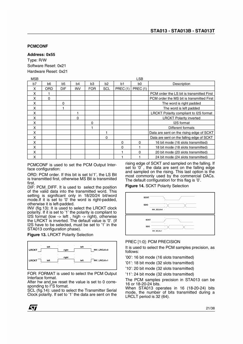
MSB LSBb7 b6 b5 b4 b3 b2 b1 b0 DescriptionX ORD DIF INV FOR SCL PREC (1) PREC (1)X 1 PCM order the LS bit is transmitted FirstX 0 PCM order the MS bit is transmitted FirstX 0 The word is right paddedX 1 The word is left paddedX 1 LRCKT Polarity compliant to I2S formatX 0 LRCKT Polarity invertedX 0 I2S formatX 1 Different formatsX 1 Data are sent on the rising edge of SCKTX 0 Data are sent on the falling edge of SCKTX 0 0 16 bit mode (16 slots transmitted)X 0 1 18 bit mode (18 slots transmitted)X 1 0 20 bit mode (20 slots transmitted)X 1 1 24 bit mode (24 slots transmitted)
PCMCONF is used to set the PCM Output Inter-face configuration:ORD: PCM order. If this bit is set to’1’, the LS Bitis transmitted first, otherwise MS Bit is transmiitedfirst.DIF: PCM_DIFF. It is used to select the positionof the valid data into the transmitted word. Thissetting is significant only in 18/20/24 bit/wordmode.If it is set to ’0’ the word is right-padded,otherwise it is left-padded.INV (fig.13): It is used to select the LRCKT clockpolarity. If it is set to ’1’ the polarity is compliant toI2S format (low -> left , high -> right), otherwisethe LRCKT is inverted. The default value is ’0’. (ifI2S have to be selected, must be set to ’1’ in theSTA013 configuration phase).
FOR: FORMAT is used to select the PCM OutputInterface format.After hw and sw reset the value is set to 0 corre-sponding to I2S format.SCL (fig.14): used to select the Transmitter SerialClock polarity. If set to ’1’ the data are sent on the
rising edge of SCKT and sampled on the falling. Ifset to ’0’ , the data are sent on the falling edgeand sampled on the rising. This last option is themost commonly used by the commercial DACs.The default configuration for this flag is ’0’.
PREC [1:0]: PCM PRECISIONIt is used to select the PCM samples precision, asfollows:’00’: 16 bit mode (16 slots transmitted)’01’: 18 bit mode (32 slots transmitted)’10’: 20 bit mode (32 slots transmitted)’11’: 24 bit mode (32 slots transmitted)The PCM samples precision in STA013 can be16 or 18-20-24 bits.When STA013 operates in 16 (18-20-24) bitsmode, the number of bits transmitted during aLRCLT period is 32 (64).
STA013 can extract max 56 bytes/MPEG frame.To know the number of A.D. bits available everyMPEG frame, the ANCCOUNT_L and ANC-COUNT_H registers (0x41 and 0x42) have to beread.The buffer dimension is 5 bytes, written bySTA013 core in sequential order. The timing in-formation to read the buffer can be obtained byreading the FRAME_CNT registers (0x67 - 0x69).To fill up the buffer with a new 5-bytes slot, theSTA013 waits until a CMD_INTERRUPT registeris written by the master.
The register contains the values for PLL X divider(see Fig. 7).
The value is changed by the internal STA013Core, to set the clocks frequencies, according tothe incoming bitstream. This value can be evenset by the user to select the PCM interface con-figuration.The VCO output frequency is divided by (X+1).This register is a reference for 32KHz and 48 KHzinput bitstream.
This register is used to select the operating modefor OCLK clock signal.If it is set to ’1’, the OCLK frequency is fixed, andit is mantained to the value fixed by the user evenif the sampling frequency of the incoming bit-stream changes.It the MODE flag is set to ’0’, the OCLK frequencychanges, and can be set to (512, 384, 256) * Fs.The default configuration for this mode is 256 *Fs.When this mode is selected, the default OCLKfrequency is 12.288 MHz.
The registers are considered logically concate-nated and contain the fractional values for thePLL, used to select the internal configuration.After Reset, the values are NA, and the opera-tional setting are done when the MPEG synchro-nisation is achieved.The following formula describes the relationshipsamong all the STA013 fractional PLL parameters:
OCLK_Freq =
1X + 1
⋅
MCLK_freqN + 1
⋅
M + 1 +
FRAC65536
where:FRAC=256 x FRAC_H + FRAC_L (decimal)These registers are a reference for 48 / 24 / 12 /32 / 16 / 8KHz audio.
The three registers are considered logically con-catenated and compose the Global FrameCounter as described in the table.It is updated at every decoded MPEG Frame.The registers are reset on both hardware andsoftware reset.
AVERAGE_BITRATE is a read-only register andit contains the average bitrate of the incoming bit-stream. The value is rounded with an accuracy of1 Kbit/sec.
SOFTVERSION
Address: 0x71Type: RO
MSB LSB
b7 b6 b5 b4 b3 b2 b1 b0
SV7 SV6 SV5 SV4 SV3 SV2 SV1 SV0
After the STA013 boot, this register contains theversion code of the embedded software.
Setting this register to 1, STA013 leaves the idlestate, starting the decoding process.The Microcontroller is allowed to set the RUNflag, once all the control registers have been in-itialized.
The registers TREBLE_FREQUENCY-HIGH andTREBLE_FREQUENCY-LOW, logically concate-nated as a 16 bit wide register, are used to selectthe frequency, in Hz, where the selected fre-quency is +12dB respect to the stop band.By setting these registers, the following rule mustbe kept:Treble_Freq < Fs/2
The registers BASS_FREQUENCY_HIGH andBASS_FREQUENCY_LOW, logically concate-nated as a 16 bit wide register, are used to selectthe frequency, in Hz, where the selected fre-quency is -12dB respect to the pass-band. Bysetting the BASS_FREQUENCY registers, thefollowing rules must be kept:
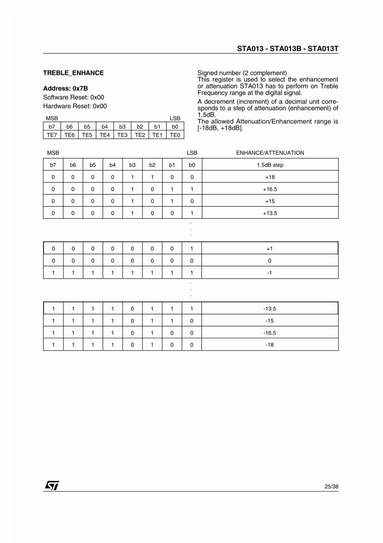
Signed number (2 complement)This register is used to select the enhancementor attenuation STA013 has to perform on TrebleFrequency range at the digital signal.A decrement (increment) of a decimal unit corre-sponds to a step of attenuation (enhancement) of1.5dB.The allowed Attenuation/Enhancement range is[-18dB, +18dB].
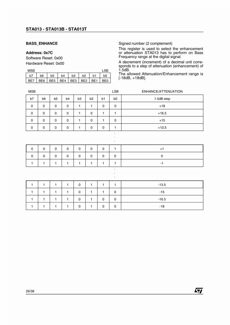
Signed number (2 complement)This register is used to select the enhancementor attenuation STA013 has to perform on BassFrequency range at the digital signal.A decrement (increment) of a decimal unit corre-sponds to a step of attenuation (enhancement) of1.5dB.The allowed Attenuation/Enhancement range is[-18dB, +18dB].
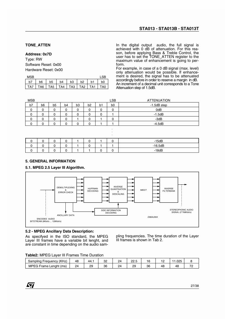
In the digital output audio, the full signal isachieved with 0 dB of attenuation. For this rea-son, before applying Bass & Treble Control, theuser has to set the TONE_ATTEN register to themaximum value of enhancement is going to per-form.For example, in case of a 0 dB signal (max. level)only attenuation would be possible. If enhance-ment is desired, the signal has to be attenuatedaccordingly before in order to reserve a margin in dB.An increment of a decimal unit corresponds to a ToneAttenuation step of 1.5dB.
5.2 - MPEG Ancillary Data Description:As specifyed in the ISO standard, the MPEGLayer III frames have a variable bit lenght, andare constant in time depending on the audio sam-
pling frequencies. The time duration of the LayerIII frames is shown in Tab 2.
Since the content of Ancillary Data into an MPEGFrame STA013 can extract is max. 56 bytes, a
specific register, to require the new 5 byte slot toSTA003 is needed.This register is:
0x16 CMD_INTERRUPT
The interrupt register, is sensitive to any non-zerovalue written by the Microcontroller. When thisregister is updated the Ancillary Data buffer isfilled up with new values and the registers
0x41 ANCCOUNT_L0x42 ANCCOUNT_H
are updated (decremented) accordingly.
5.3. I/O CELL DESCRIPTION1) CMOS Tristate Output Pad Buffer, 4mA, with Slew Rate Control / Pin numbers 9, 10, 11, 20, 28
EN
A
D98AU904
Z OUTPUT PIN MAX LOAD
Z 100pF
2) CMOS Bidir Pad Buffer, 4mA, with Slew Rate Control / Pin numbers 3, 12
THE OVERALLSETTING STEPSARE INCLUDED INTHE STA013CONFIGURATIONFILE AND CANBE DOWNLOADEDIN ONE STEP.STM PROVIDESA SPECIFICCONFIGURATIONFILE FOR EACHSUPPORTEDINPUT CLOCKFREQUENCY
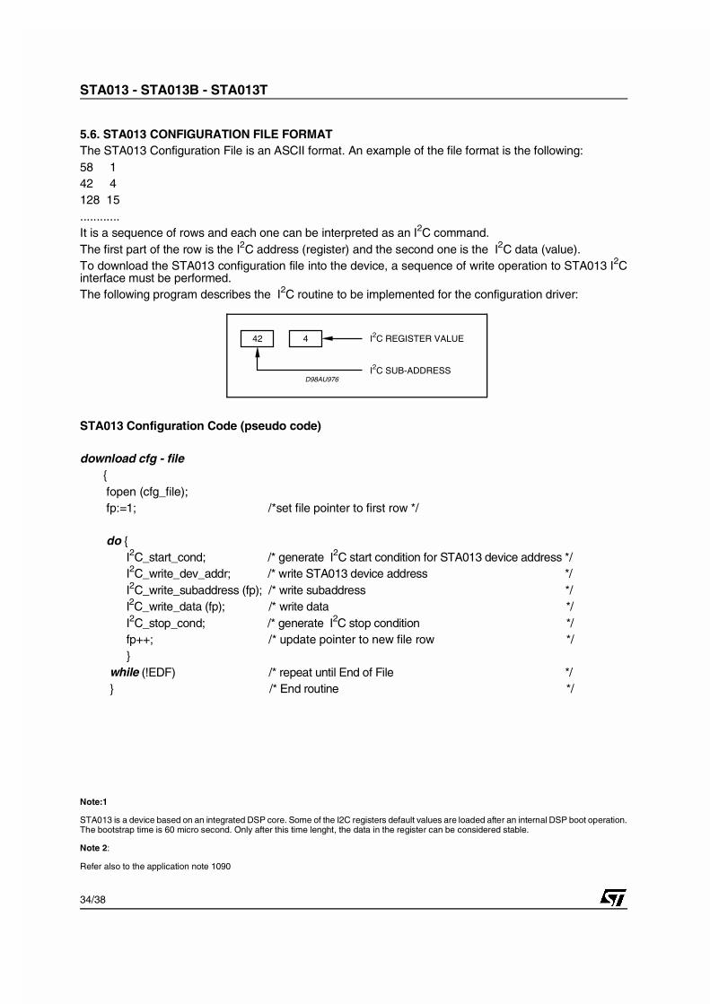
5.6. STA013 CONFIGURATION FILE FORMATThe STA013 Configuration File is an ASCII format. An example of the file format is the following:58 142 4128 15............It is a sequence of rows and each one can be interpreted as an I2C command.The first part of the row is the I2C address (register) and the second one is the I2C data (value).To download the STA013 configuration file into the device, a sequence of write operation to STA013 I2Cinterface must be performed.The following program describes the I2C routine to be implemented for the configuration driver:
STA013 Configuration Code (pseudo code)
download cfg - file fopen (cfg_file); fp:=1; /*set file pointer to first row */ do I2C_start_cond; /* generate I2C start condition for STA013 device address */ I2C_write_dev_addr; /* write STA013 device address */ I2C_write_subaddress (fp); /* write subaddress */ I2C_write_data (fp); /* write data */ I2C_stop_cond; /* generate I2C stop condition */ fp++; /* update pointer to new file row */ while (!EDF) /* repeat until End of File */ /* End routine */
42 4 I2C REGISTER VALUE
I2C SUB-ADDRESSD98AU976
Note:1
STA013 is a device based on an integrated DSP core. Some of the I2C registers default values are loaded after an internal DSP boot operation.The bootstrap time is 60 micro second. Only after this time lenght, the data in the register can be considered stable.
Note 2:
Refer also to the application note 1090
STA013 - STA013B - STA013T
34/38
SO28
DIM.mm inch
MIN. TYP. MAX. MIN. TYP. MAX.
A 2.65 0.104
a1 0.1 0.3 0.004 0.012
b 0.35 0.49 0.014 0.019
b1 0.23 0.32 0.009 0.013
C 0.5 0.020
c1 45° (typ.)
D 17.7 18.1 0.697 0.713
E 10 10.65 0.394 0.419
e 1.27 0.050
e3 16.51 0.65
F 7.4 7.6 0.291 0.299
L 0.4 1.27 0.016 0.050
S 8 ° (max.)
OUTLINE ANDMECHANICAL DATA
STA013 - STA013B - STA013T
35/38
OUTLINE ANDMECHANICAL DATA
DIM.mm inch
MIN. TYP. MAX. MIN. TYP. MAX.
A 1.60 0.063
A1 0.05 0.15 0.002 0.006
A2 1.35 1.40 1.45 0.053 0.055 0.057
B 0.30 0.37 0.45 0.012 0.015 0.018
C 0.09 0.20 0.004 0.008
D 11.80 12.00 12.20 0.464 0.472 0.480
D1 9.80 10.00 10.20 0.386 0.394 0.401
D3 8.00 0.315
E 11.80 12.00 12.20 0.464 0.472 0.480
E1 9.80 10.00 10.20 0.386 0.394 0.401
E3 8.00 0.315
e 0.80 0.031
L 0.45 0.60 0.75 0.018 0.024 0.030
L1 1.00 0.039
k 0˚(min.), 3.5˚(typ.), 7˚(max.)
TQFP44 (10 x 10 x 1.4mm)
A
A2A1
B
Seating Plane
C
11
12
22
2333
34
44
E1 E
D1
D
e
1
K
B
TQFP4410
L
0.10mm
.004
0076922 D
STA013 - STA013B - STA013T
36/38
OUTLINE ANDMECHANICAL DATA
D1 D
A
0.15
A1
A2e
f
f
A
12345678
B
C
D
E
F
G
H
E1
φ b (64 PLACES)
E
BALL 1 IDENTIFICATION
LFBGA64M
DIM.
mm inch
MIN. TYP. MAX. MIN. TYP. MAX.
A 1.700 0.067
A1 0.350 0.400 0.450 0.014 0.016 0.018
A2 1.100 0.043
b 0.500 0.20
D 8.000 0.315
D1 5.600 0.220
e 0.800 0.031
E 8.000 0.315
E1 5.600 0.220
f 1.200 0.047
LFBGA64
Body: 8 x 8 x 1.7mm
STA013 - STA013B - STA013T
37/38
Information furnished is believed to be accurate and reliable. However, STMicroelectronics assumes no responsibility for the consequencesof use of such information nor for any infringement of patents or other rights of third parties which may result from its use. No license isgranted by implication or otherwise under any patent or patent rights of STMicroelectronics. Specifications mentioned in this publication aresubject to change without notice. This publication supersedes and replaces all information previously supplied. STMicroelectronics productsare not authorized for use as critical components in life support devices or systems without express written approval of STMicroelectronics.
The ST logo is a registered trademark of STMicroelectronics.All other names are the property of their respective owners
STMicroelectronics GROUP OF COMPANIESAustralia – Belgium - Brazil - Canada - China – Czech Republic - Finland - France - Germany - Hong Kong - India - Israel - Italy - Japan -
Malaysia - Malta - Morocco - Singapore - Spain - Sweden - Switzerland - United Kingdom - United Stateswww.st.com