Logic design lab manual 3 rd sem M.S ENGINEERING COLLEGE NAVARTNA AGRAHARA, BANGALORE-562110 Department of Electronics and Communication Logic design Lab [10ESL38] III SEM Prepared by: Naveen H Pavitra Dept of ECE, MSEC 2014-2015 Page | 1
Transcript
Logic design lab manual 3rdsem
M.S ENGINEERING COLLEGE
NAVARTNA AGRAHARA, BANGALORE-562110
Department of Electronics and Communication
Logic design Lab [10ESL38]
III SEM
Prepared by:
Naveen H
Pavitra
Dept of ECE, MSEC 2014-2015 Page | 1
Logic design lab manual 3rdsem
Sl.no Table of contents Page no.
1. a)Verification of logic gates.
b)Simplification, realization of Boolean expressions using logic
gates/Universal gates.
1
2. Realization of Half/Full adder and Half/Full Subtractors using logic gates. 8
3. (i) Realization of parallel adder/Subtractors using 7483 chip
ii) BCD to Excess-3 code conversion and vice versa.
14
4. Realization of Binary to Gray code conversion and vice versa 20
5. MUX/DEMUX – use of 74153, 74139 for arithmetic circuits and
codeconverter.
25
6. Realization of One/Two bit comparator and study of 7485 magnitude
comparator. 30
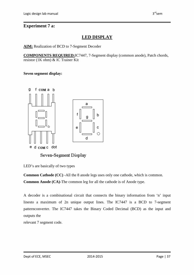
7. Use of a) Decoder chip to drive LED display and
b) Priority encoder.
34
8. Truth table verification of Flip-Flops:
(i) JK Master slave
(ii) T type and
(iii) D type.
39
9. Realization of 3 bit counters as a sequential circuit and MOD – N counter
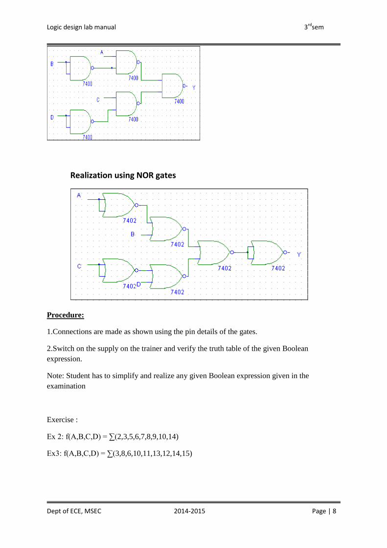
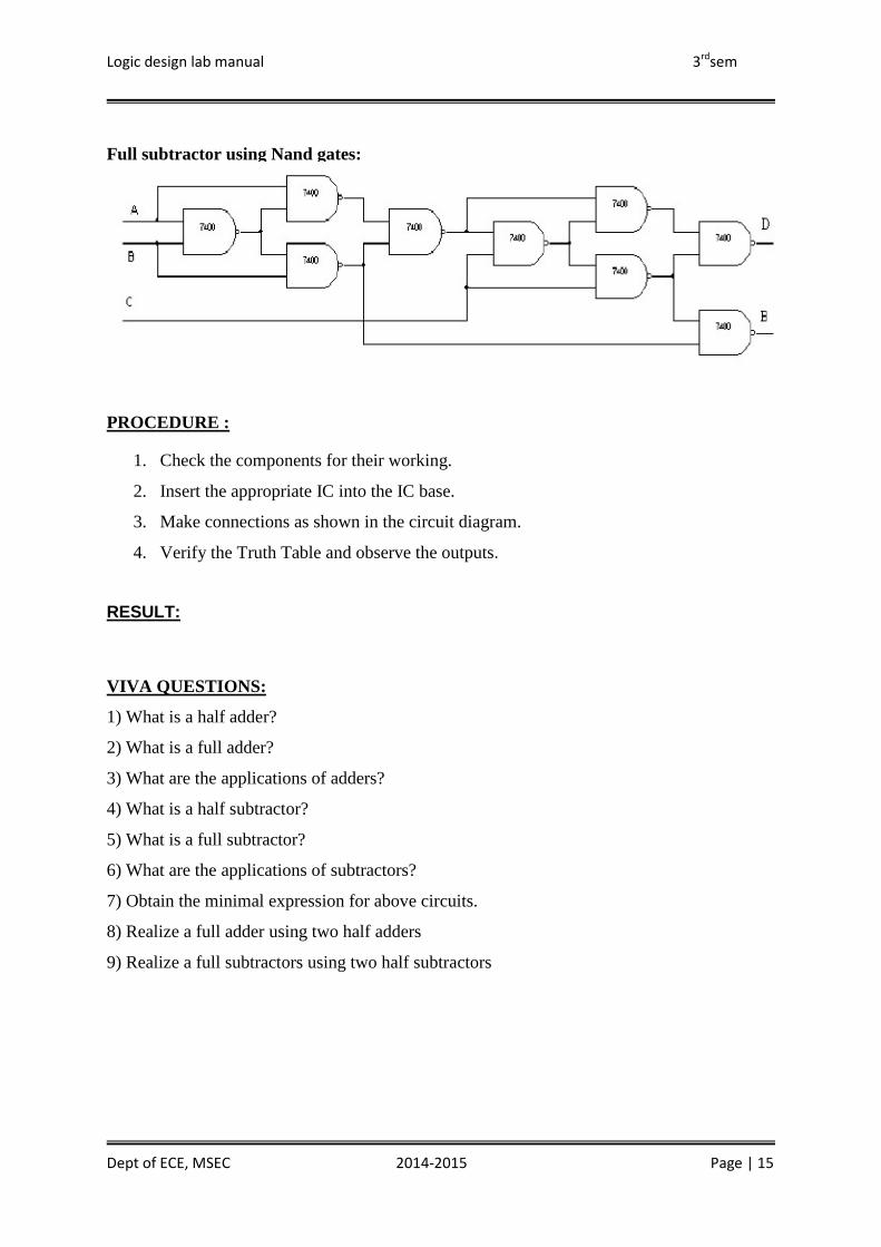
3. Make connections as shown in the circuit diagram.
4. Verify the Truth Table and observe the outputs.
RESULT:
VIVA QUESTIONS:
1) What is a half adder?
2) What is a full adder?
3) What are the applications of adders?
4) What is a half subtractor?
5) What is a full subtractor?
6) What are the applications of subtractors?
7) Obtain the minimal expression for above circuits.
8) Realize a full adder using two half adders
9) Realize a full subtractors using two half subtractors
Dept of ECE, MSEC 2014-2015 Page | 15
Logic design lab manual 3rdsem
Experiment 3:
PARALLEL ADDER/SUBTRACTOR USING 7483 AND BCD TO
EXCESS-3 CODE AND VICE VERSA i) Parallel adder/subtractor using 7483
AIM:i)To design and set up the following circuit using IC 7483.
a) A 4-bit binary parallel adder.
b)A 4-bit binary parallel subtractor.
COMPONENTS REQUIRED:IC 7483, IC 7486, Patch Cords & IC Trainer Kit.
THEORY: The Full adder can add single-digit binary numbers and carries. The largest sum
that can be obtained using a full adder is 112. Parallel adders can add multiple-digit numbers.
If full adders are placed in parallel, we can add two- or four-digit numbers or any other size
desired.
Pin details:
Here A1 A2 A3 A4 & B1 B2 B3 B4 &Cinare the inputs.S1S2S3S4&Coutare the outputs.
Dept of ECE, MSEC 2014-2015 Page | 16
Logic design lab manual 3rdsem
1) 4 bit adder operation
If control input Cin = 0, addition can be performed.
Ex a) if A1 A2 A3 A4 = 1100 Cin = 0 B1 B2 B3 B4 = 0011 Then sum,
S1 S2 S3 S4 = 1111 andCout = 0
Ex b) if A1 A2 A3 A4 = 1001 Cin = 1 B1 B2 B3 B4 = 1101 Then sum,
S1 S2 S3 S4 = 0111 andCout = 1
2) 4 bit subtraction operation using one’s and two’s complement method.
(i) 1’s complement method
If Cin =1 subtraction can be performed.
Ex a) if A1 A2 A3 A4 = 1001 B1 B2 B3 B4 = 0011 by normal subtraction Difference ,
S1 S2 S3 S4 = 0110
In one’s complement method
A1 A2 A3 A4 = 1100
B1 B2 B3 B4 = 1100 (1’s complement of 0011)
End around carry ,① 0101
+1
difference ,S1 S2 S3 S4 = 0110
ii) 2’s complement method:
2’s complement method of subtraction can be performed, if S =1 and Cin= 1
A1 A2 A3 A4 = 1100
B1 B2 B3 B4 = 1101 (2’s complement of 0011)
End around carry ,① 0110
isdisregared difference, S1 S2 S3 S4 = 0110
If end around carry is 1, the result is positive. If there is no carry the result is negative and is in 1’s complement form.
If end around carry is 1, the result is positive. If there is no carry the result is negative and is in 2’s complement form.
Dept of ECE, MSEC 2014-2015 Page | 17
Logic design lab manual 3rdsem
PROCEDURE:
1. Check all the components for their working.
2. Insert the appropriate IC into the IC base.
3. Make connections as shown in the circuit diagram.
4. Apply Minuend and subtrahend bits on A and B and cin=1.
5. Verify the results and observe the outputs.
RESULT :
ii) BCD to EXCESS-3 code and vice versa
AIM: To design and realize the following using IC 7483.
I) BCD to Excess- 3 Code
II) Excess-3 to BCD Code.
COMPONENTS REQUIRED:IC 7483, IC 7486, Patch Cords & IC Trainer Kit.
Truth table: BCD to Excess- 3 Code
Bcd code word
BCD (input) Excess -3 code
(output)
B3 B2 B1 B0 E3 E2 E1 E0
0 0 0 0 0 0 0 1 1
1 0 0 0 1 0 1 0 0
2 0 0 1 0 0 1 0 1
3 0 0 1 1 0 1 1 0
4 0 1 0 0 0 1 1 1
5 0 1 0 1 1 0 0 0
6 0 1 1 0 1 0 0 1
7 0 1 1 1 1 0 1 0
8 1 0 0 0 1 0 1 1
9 1 0 0 1 1 1 0 0
Dept of ECE, MSEC 2014-2015 Page | 18
Logic design lab manual 3rdsem
E3 = B3+B2 B0+B2 B1 E2 = B2 B1+ B2 B0 +B2 B1 B0
E1= B1⨁ B0 E0 = B0
Excess -3 to BCD code:
0 0 0 0
0 1 1 1
* * * *
1 1 * *
0 1 1 1
1 0 0 0
* * * *
0 1 * *
1 0 1 0
1 0 1 0
* * * *
1 0 * *
1 0 0 1
1 0 0 1
* * * *
1 0 * *
Excess -3 (input) Bcd code word
Bcd code (output)
E3 E2 E1 E0 B3 B2 B1 B0
0 0 1 1 0 0 0 0 0
0 1 0 0 1 0 0 0 1
0 1 0 1 2 0 0 1 0
0 1 1 0 3 0 0 1 1
0 1 1 1 4 0 1 0 0
1 0 0 0 5 0 1 0 1
1 0 0 1 6 0 1 1 0
1 0 1 0 7 0 1 1 1
1 0 1 1 8 1 0 0 0
1 1 0 0 9 1 0 0 1
B1 B0
B3 B2
B1 B0
B3 B2
B1 B0
B3 B2
B1 B0
B3 B2
Dept of ECE, MSEC 2014-2015 Page | 19
Logic design lab manual 3rdsem
B3 = E3 E2 + E3 E1 E0 B2 = E2 ⨁ E0 E1
B1 = E1 ⨁ E0 B0 = E0
Bcd to excess-3 codeNand gate:
* * 0 *
0 0 0 0
1 * * *
0 0 1 0
* * 0 *
0 0 1 0
0 * * *
1 1 0 1
* * 0 *
1 0 0 1
1 * * *
1 0 0 1
* * 0 *
0 1 0 1
0 * * *
0 1 0 1
E1 E0
E3 E2 E1 E0
E3 E2
E1 E0
E3 E2
E1 E0
E3 E2
=0
0 0 1 1
Dept of ECE, MSEC 2014-2015 Page | 20
Logic design lab manual 3rdsem
Excess -3 to BCD Code using Nand gate:
0 0 1 1
=1
Dept of ECE, MSEC 2014-2015 Page | 21
Logic design lab manual 3rdsem
PROCEDURE:
1. Check all the components for their working.
2. Insert the appropriate IC into the IC base.
3. Make connections as shown in the circuit diagram.
RESULT:
VIVA QUESTIONS:
1) What is the internal structure of 7483 IC?
2) What do you mean by code conversion?
3) What are the applications of code conversion?
4) How do you realize a subtractor using full adder?
5) What is a ripple Adder? What are its disadvantages
Dept of ECE, MSEC 2014-2015 Page | 22
Logic design lab manual 3rdsem
Experiment 4:
BINARY TO GRAY CODE AND VICE VERSA CONVERSION
AIM: To realize Binary to Gray code converter and vice versa.
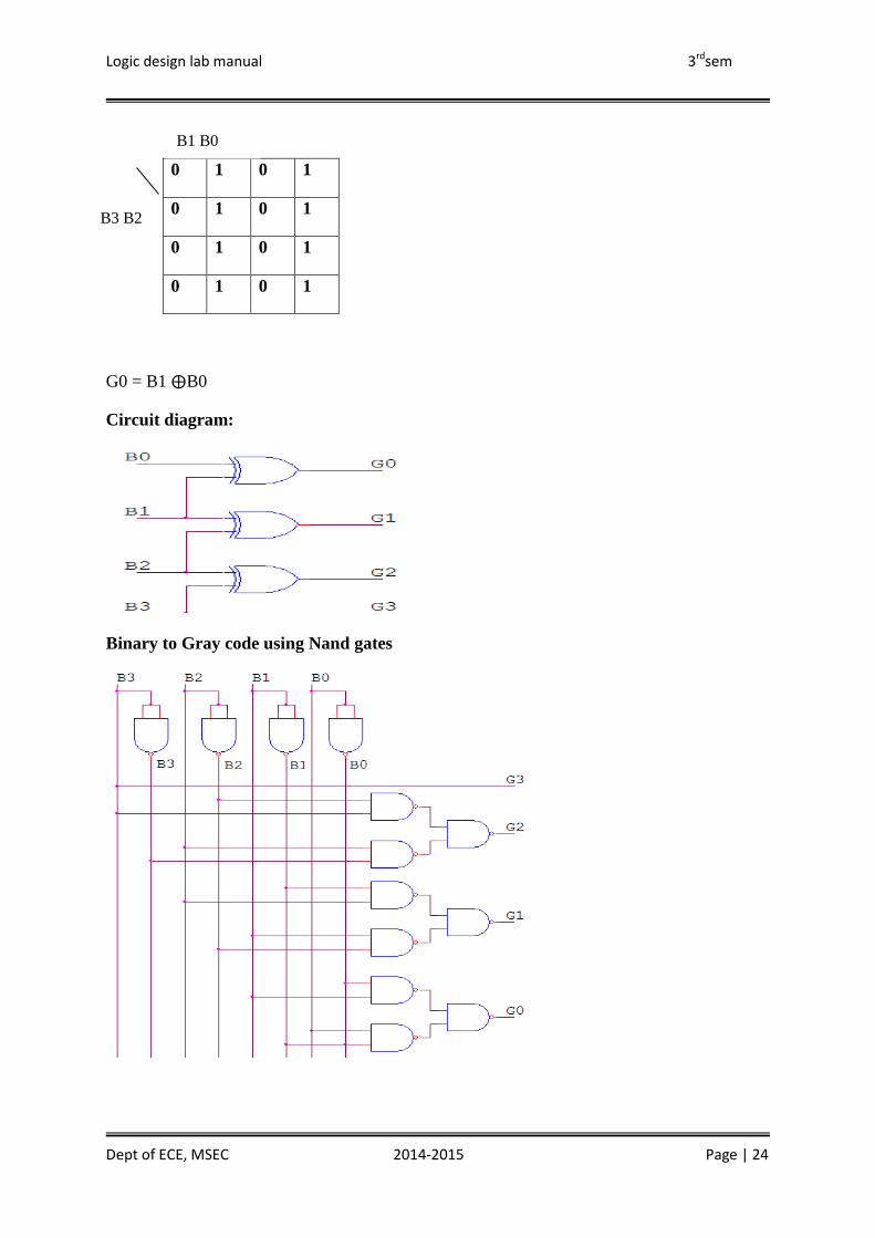
COMPONENTS REQUIRED:IC 7400, IC 7486, and IC 7408, Patch Cords & IC Trainer Kit Truth table: Binary to Gray code
G3 = B3
G2 = B3 ⨁ B2
G1 = B1 ⨁ B2
Binary code Gray code
B3 B2 B1 B0 G3 G2 G1 G0
0 0 0 0 0 0 0 0
0 0 0 1 0 0 0 1
0 0 1 0 0 0 1 1
0 0 1 1 0 0 1 0
0 1 0 0 0 1 1 0
0 1 0 1 0 1 1 1
0 1 1 0 0 1 0 1
0 1 1 1 0 1 0 0
1 0 0 0 1 1 0 0
1 0 0 1 1 1 0 1
1 0 1 0 1 1 1 1
1 0 1 1 1 1 1 0
1 1 0 0 1 0 1 0
1 1 0 1 1 0 1 1
1 1 1 0 1 0 0 1
1 1 1 1 1 0 0 0
0 0 0 0
0 0 0 0
1 1 1 1
1 1 1 1
0 0 0 0
1 1 1 1
0 0 0 0
1 1 1 1
0 0 1 1
1 1 0 0
1 1 0 0
0 0 1 1
B1 B0
B3 B2
B1 B0
B3 B2
B1 B0
B3 B2
Dept of ECE, MSEC 2014-2015 Page | 23
Logic design lab manual 3rdsem
G0 = B1 ⨁B0
Circuit diagram:
Binary to Gray code using Nand gates
0 1 0 1
0 1 0 1
0 1 0 1
0 1 0 1
B1 B0
B3 B2
Dept of ECE, MSEC 2014-2015 Page | 24
Logic design lab manual 3rdsem
Truth table: Gray to Binary code
B3 = G3
G2 = G3 ⨁ G2
B1 = G3 ⨁ G2 ⨁ G1 B0 = G3 ⨁ G2 ⨁ G1 ⨁ G0
Gray code Binary code
G3 G2 G1 G0 B3 B2 B1 B0
0 0 0 0 0 0 0 0
0 0 0 1 0 0 0 1
0 0 1 1 0 0 1 0
0 0 1 0 0 0 1 1
0 1 1 0 0 1 0 0
0 1 1 1 0 1 0 1
0 1 0 1 0 1 1 0
0 1 0 0 0 1 1 1
1 1 0 0 1 0 0 0
1 1 0 1 1 0 0 1
1 1 1 1 1 0 1 0
1 1 1 0 1 0 1 1
1 0 1 0 1 1 0 0
1 0 1 1 1 1 0 1
1 0 0 1 1 1 1 0
1 0 0 0 1 1 1 1
0 0 0 0
0 0 0 0
1 1 1 1
1 1 1 1
0 0 0 0
1 1 1 1
0 0 0 0
1 1 1 1
0 1 0 1
1 0 1 0
0 1 0 1
1 0 1 0
0 0 1 1
1 1 0 0
0 0 1 1
1 1 0 0
G1 G0
G3 G2
G1 G0
G3 G2
G1 G0
G3 G2
G1 G0
G3 G2
Dept of ECE, MSEC 2014-2015 Page | 25
Logic design lab manual 3rdsem
Circuit diagram:
Gray to Binary code using Nand gates:
Dept of ECE, MSEC 2014-2015 Page | 26
Logic design lab manual 3rdsem
PROCEDURE:
1. Check all the components for their working. 2. Insert the appropriate IC into the IC base. 3. Make connections as shown in the circuit diagram. 4. Verify the Truth Table and observe the outputs.
RESULT:
VIVA QUESTIONS:
1) What are code converters?
2) What is the necessity of code conversions?
3) What is gray code?
4) Realize the Boolean expressions for
a) Binary to gray code conversion
b) Gray to binary code conversion
Dept of ECE, MSEC 2014-2015 Page | 27
Logic design lab manual 3rdsem
Experiment 5:
MULTIPLEXER / DE-MULTIPLEXER – 74153, 74139
AIM:Relization of MUX and De-MUX circuit and use of 74153, 74139 for airthmetics circuits and code converter.
COMPONENTS REQUIRED:IC 7400, IC 7410, IC 7420, IC 7404, IC 74153, IC 74139, Patch Cords & IC Trainer Kit.
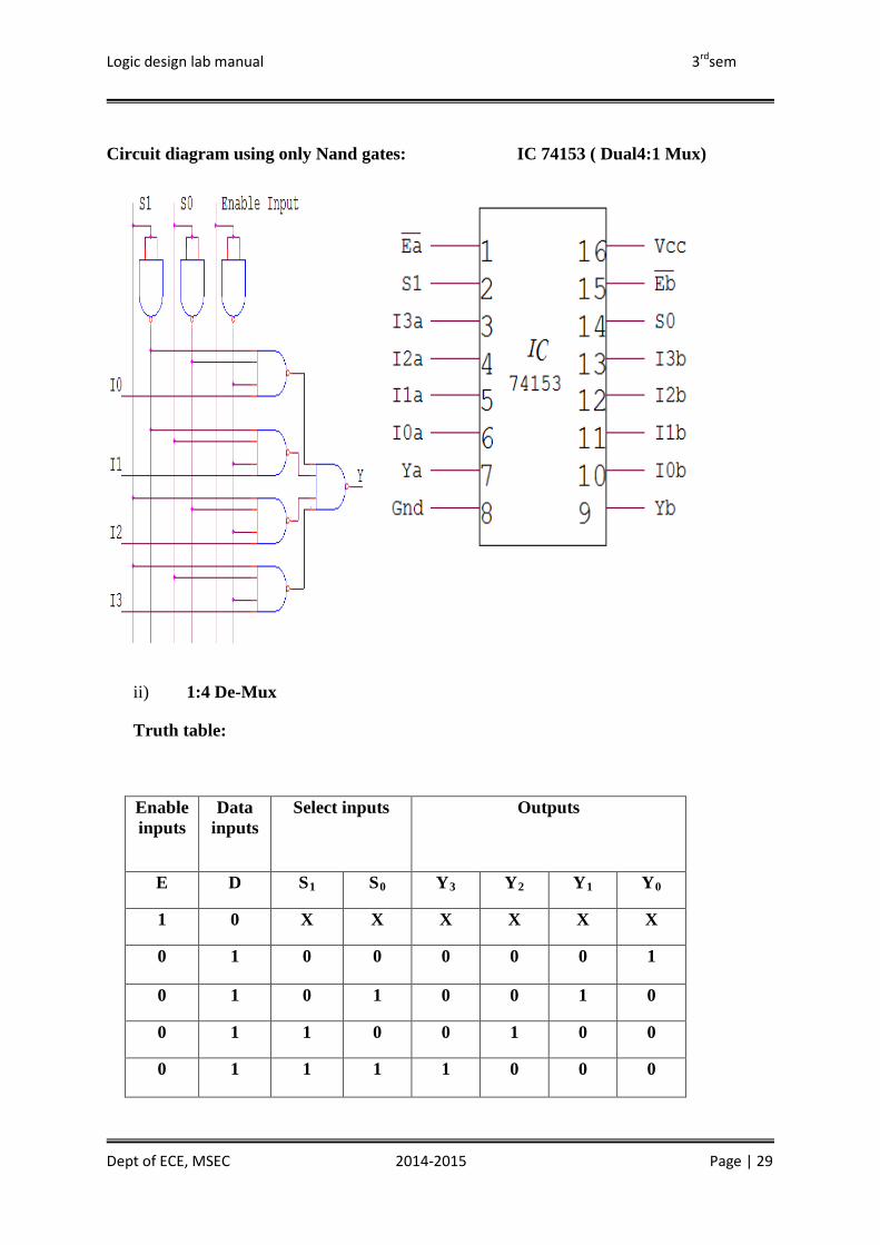
i) 4:1 Mux Truth table:
Select inputs
Enable inputs
Inputs Output
S1 S0 E’ I0 I1 I2 I3 Y
X X 1 X X X X 0
0 0 0 0 X X X 0
0 0
0 1 X X X 1
0 1 0 X 0 X X 0
0 1 0 X 1 X X 1
1 0 0 X X 0 X 0
1 0 0 X X 1 X 1
1 1 0 X X X 0 0
1 1 0 X X X 1 1
Dept of ECE, MSEC 2014-2015 Page | 28
Logic design lab manual 3rdsem
Circuit diagram using only Nand gates: IC 74153 ( Dual4:1 Mux)
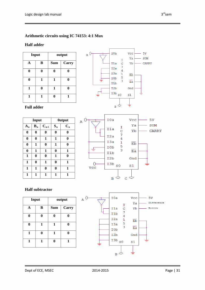
ONE / TWO BIT COMPARATORS 7485 MAGNITUDE COMPARATOR
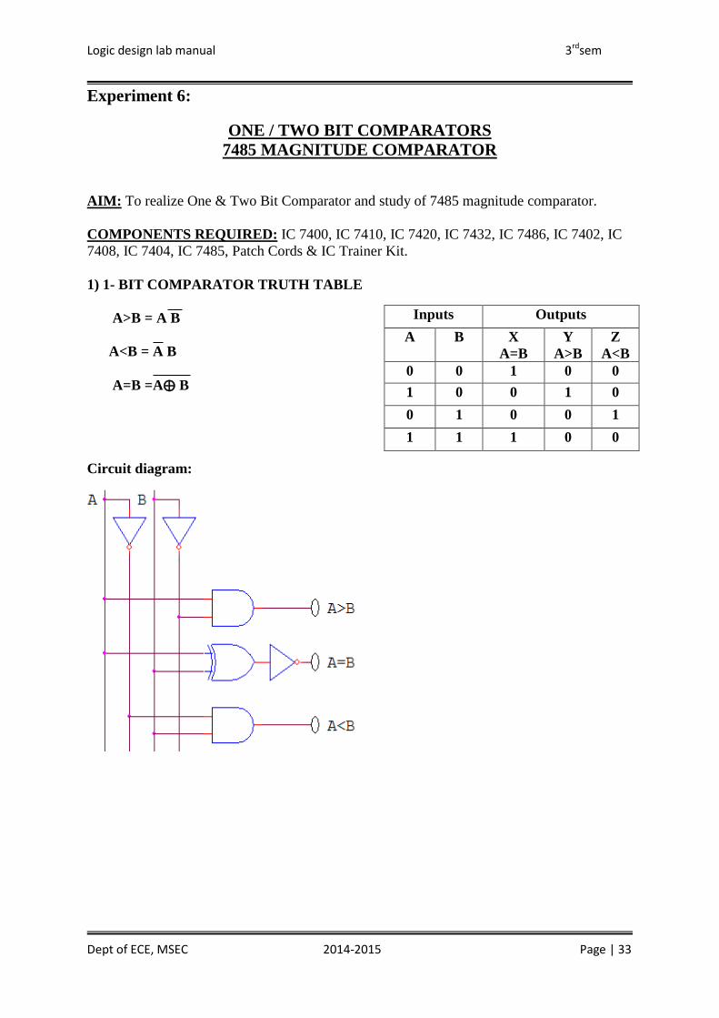
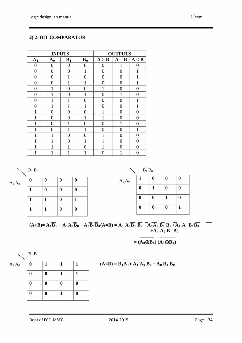
AIM: To realize One & Two Bit Comparator and study of 7485 magnitude comparator. COMPONENTS REQUIRED: IC 7400, IC 7410, IC 7420, IC 7432, IC 7486, IC 7402, IC 7408, IC 7404, IC 7485, Patch Cords & IC Trainer Kit. 1) 1- BIT COMPARATOR TRUTH TABLE A>B = A B A<B = A B A=B =A⨁ B Circuit diagram:
2. The supply and ground connection are made to the IC i.e. pin no. 8 is connected to
ground and pin no.16 is connected to +VCC(+5v)
3. Feed the 4-bit binary patterns A,B,C, and D using logic input switches.
4. Connect the outputs of the decoder chip to the corresponding pins of the seven
segment display.
5. Connect +5V to the seven segment LED since we are using a common anode
LED.
6. Monitor the output on the &-segment LED according to the truth table.
7. Verify the output according to the truth table.
RESULTS : VIVA QUESTIONS:
1. What are the different types of LEDs?
2. Draw the internal circuit diagram of an LED.
3. What are the applications of LEDs?
Dept of ECE, MSEC 2014-2015 Page | 39
Logic design lab manual 3rdsem
Experiment 7 b:
PRIORITY ENCODER
AIM :To setup a circuit of priority encoder
COMPONENTS REQUIRED:IC 74147, Patch chords & IC Trainer Kit
DESIGN: DECIMAL-TO BCD ENCODER USING IC 74147.
Truth table:
Inputs Outputs
I 1 I 2 I 3 I 4 I 5 I 6 I 7 I 8 I 9 A 3 A 2 A 1 A 0
1 1 1 1 1 1 1 1 0 0 1 1 0
X X X X X X X 0 1 0 1 1 1
X X X X X X 0 1 1 1 0 0 0
X X X X X 0 1 1 1 1 0 0 1
X X X X 0 1 1 1 1 1 0 1 0
X X X 0 1 1 1 1 1 1 0 1 1
X X 0 1 1 1 1 1 1 1 1 0 0
X 0 1 1 1 1 1 1 1 1 1 0 1
0 1 1 1 1 1 1 1 1 1 1 1 0
1 1 1 1 1 1 1 1 1 1 1 1 1
Dept of ECE, MSEC 2014-2015 Page | 40
Logic design lab manual 3rdsem
PROCEDURE :
1. Setup the circuit as shown in the circuit diagram.
2. Give supply to the trainer kit and feed the active low input combinations.
3. Obseve the active low output corresponding tp active low inut combinations and
verify the truth table
RESULT :
VIVA QUESTIONS:
1. What is a priority encoder?
2. What is the role of an encoder in communication?
3. What is the advantage of using an encoder?
4. What are the uses of validating outputs?
Dept of ECE, MSEC 2014-2015 Page | 41
Logic design lab manual 3rdsem
Experiment 8:
VERIFICATION OF FLIP FLOPS
AIM:To design and verify the truth table of JK master slave, T type and D type flip flops.
COMPONENTS REQUIRED:IC 7408, IC 7404, IC 7402, IC 7400, Patch Cords & IC Trainer Kit. THEORY:Logic circuits that incorporate memory cells are called sequential logic circuits; their outputdepends not only upon the present value of the input but also upon the previous values.Sequential logic circuits often require a timing generator (a clock) for their operation. The latch (flip-flop) is a basic bi-stable memory element widely used in sequential logic circuits. Usually there are two outputs, Q and its complementary value. Circuit Diagram:
Truth table and logic diagram:
PRE CLR CLK J K Q+ Q’+ COMMENTS 1 1 1 X X Q Q’ ENABLED 0 1 0 X X 0 1 RESET 1 0 0 X X 1 0 PRESET 1 1 0 X 0 Q Q’ NO CHANGE 1 1 0 0 Q Q’ NO CHANGE 1 1 0 1 0 1 RESET 1 1 1 0 1 0 SET
1 1 1 1 Q’ Q TOGGLE
Dept of ECE, MSEC 2014-2015 Page | 42
Logic design lab manual 3rdsem
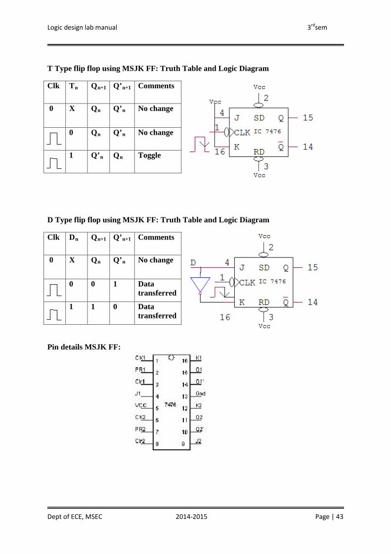
T Type flip flop using MSJK FF: Truth Table and Logic Diagram
D Type flip flop using MSJK FF: Truth Table and Logic Diagram
Pin details MSJK FF:
Clk Tn Qn+1 Q’n+1 Comments
0 X Qn Q’n No change
0 Qn Q’n No change
1 Q’n Qn Toggle
Clk Dn Qn+1 Q’n+1 Comments
0 X Qn Q’n No change
0 0 1 Data transferred
1 1 0 Data transferred
Dept of ECE, MSEC 2014-2015 Page | 43
Logic design lab manual 3rdsem
PROCEDURE :
1. Connections are made as shown in the circuit diagram. 2. Switch on the power supply of the IC trainer kit. 3. Truth tables of ‘MSJK’ FF, ‘T’ FF and ‘D’ FF are verified.
RESULT :
VIVA QUESTIONS:
1. WHAT IS THE DIFFERENCE BETWEEN FLIP-FLOP & LATCH?
2. GIVE EXAMPLES FOR SYNCHRONOUS & ASYNCHRONOUS INPUTS?
3. WHAT ARE THE APPLICATIONS OF DIFFERENT FLIP-FLOPS?
4. WHAT IS THE ADVANTAGE OF EDGE TRIGGERING OVER LEVEL
TRIGGERING?
5. WHAT IS THE RELATION BETWEEN PROPAGATION DELAY & CLOCK
FREQUENCY OF FLIP-FLOP?
6. WHAT IS RACE AROUND IN FLIP-FLOP & HOW TO OVER COME IT?
7. CONVERT THE J K FLIP-FLOP INTO D FLIP-FLOP AND T FLIP-FLOP?
8. LIST THE FUNCTIONS OF ASYNCHRONOUS INPUTS?
Dept of ECE, MSEC 2014-2015 Page | 44
Logic design lab manual 3rdsem
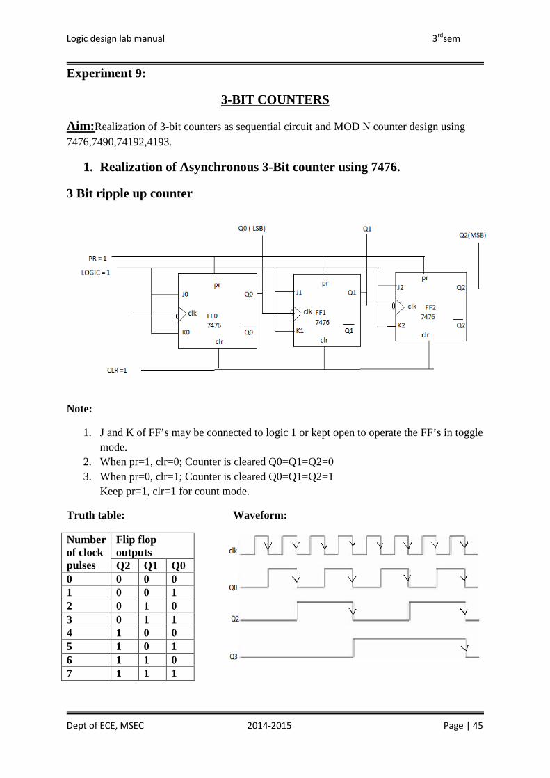
Experiment 9:
3-BIT COUNTERS
Aim:Realization of 3-bit counters as sequential circuit and MOD N counter design using 7476,7490,74192,4193.
1. Realization of Asynchronous 3-Bit counter using 7476.
3 Bit ripple up counter
Note:
1. J and K of FF’s may be connected to logic 1 or kept open to operate the FF’s in toggle mode.
2. When pr=1, clr=0; Counter is cleared Q0=Q1=Q2=0 3. When pr=0, clr=1; Counter is cleared Q0=Q1=Q2=1
2)Design and realization of 3-bit synchronous counter:
Design steps:
1) Count table 2) excitation table
Present state output
Next state output
J K
0 0 0 X
0 1 1 X
1 0 X 1
1 1 X 0
3) sequence table
Present state Next state Flip fop inputs Qc Qb Qa Qc+ Qb+ Qa+ J2 K2 J1 K1 J0 K0 0 0 0 0 0 1 0 X 0 X 1 X 0 0 1 0 1 0 0 X 1 X X 1 0 1 0 0 1 1 0 X X 0 1 X 0 1 1 1 0 0 1 X X 1 X 1 1 0 0 1 0 1 X 0 0 X 1 X 1 0 1 1 1 0 X 0 1 X X 1 1 1 0 1 1 1 X 0 X 0 1 X 1 1 1 0 0 0 X 1 X 1 X 1
1. Make the connections as shown in the circuit diagram. 2. Keep preset and clear at logic 1 for count mode after clearing all flip flops. 3. Apply clock pulse and verify the truth table as shown. 4. Apply a continue clock of frequency f=1Khz or 10 Khz and observe the output
1. To start the count sequence from QaQBQcQd = 0000, S1 and S2 are connected to ground. R1 and R2 are connected to logic 1 level, then connected to logic 0 level for count mode.
2. Clock input is given to input ‘A’ and output Qa& input ‘B’ are shorted, then it acts as A divided by 10 counter for BCD count sequence.
3. Verify the truth table and observe the output waveforms.
1. To start the count sequence from QaQBQcQd = 0000, S1 and S2 are connected to ground. R1 is connected to Qa and R2 is connected to Qc , for count mode.
2. Clock input is given to input ‘A’ and output Qa& input ‘B’ are shorted, then it acts as A divided by 5 counter for MOD 5 count sequence.
3. Verify the truth table and observe the output waveforms.
RESULT :
VIVA QUESTIONS:
1. What is the difference between Flip-Flop & latch? 2. Give examples for synchronous & asynchronous inputs? 3. What are the applications of different Flip-Flops? 4. What is the advantage of Edge triggering over level triggering? 5. What is the relation between propagation delay & clock frequency of flip-flop? 6. What is race around in flip-flop & how to over come it? 7. Convert the J K Flip-Flop into D flip-flop and T flip-flop? 8. List the functions of asynchronous inputs?
Dept of ECE, MSEC 2014-2015 Page | 50
Logic design lab manual 3rdsem
Experiment 10:
SHIFT REGISTERS
AIM: To realize and study of Shift Register.
1) SISO (Serial in Serial out)
2) SIPO (Serial in Parallel out) 3) PIPO (Parallel in Parallel out)
4) PISO (Parallel in Serial out)
COMPONENTS REQUIRED: IC 7495, Patch Cords & IC Trainer Kit.
PIN Details:
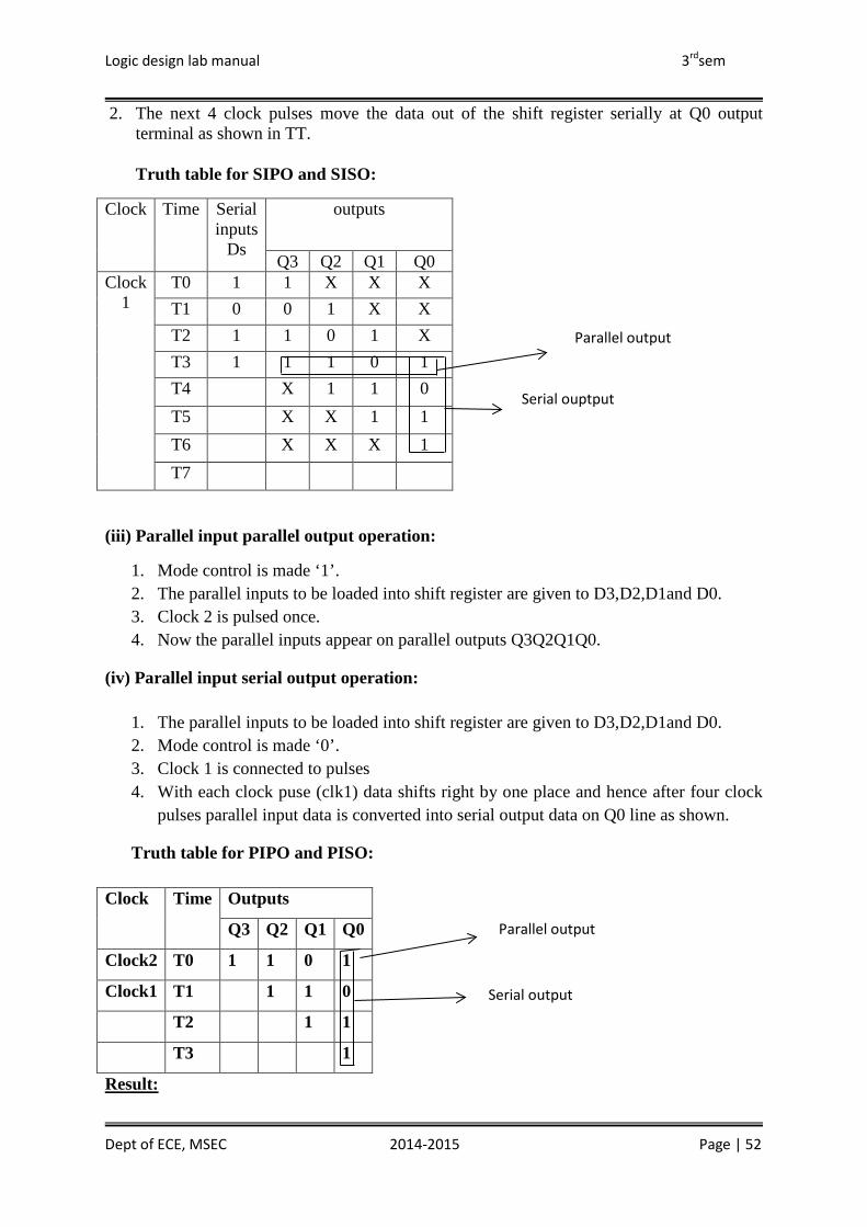
Note : Ds – serial input data ( to be right shifted) D3,D2,D1,D0 – Parallel data inputs to be loaded into the shift register. M – mode control Keep M = 1 for loading parallel data and to enable clock 2. Keep M =0 for enabling c\lock 1. Clock 2 – for loading parallel input data and for shift left of data. Clock 1 – for right shift of data. Q3,Q2,Q1,Q0 – Parallel output of the shift register. (i)Serial input parallel output operation: To perform SIPO operation consider a 4-bit data say 1101. Following steps are used here:
1. Mode control is made ‘0’. 2. Clock 1 is connected to pulses. 3. The serial input is given to Ds. 4. After four clock pulses the serial input data appears in parallel form as Q3Q2Q1Q0 as
shown in TT. (ii)Serial input Serial output operation: 1. Steps 1 to 4 of SIPO operation is repeated.
Dept of ECE, MSEC 2014-2015 Page | 51
Logic design lab manual 3rdsem
2. The next 4 clock pulses move the data out of the shift register serially at Q0 output terminal as shown in TT. Truth table for SIPO and SISO:
Clock Time Serial inputs
Ds
outputs
Q3 Q2 Q1 Q0 Clock
1 T0 1 1 X X X T1 0 0 1 X X T2 1 1 0 1 X T3 1 1 1 0 1 T4 X 1 1 0 T5 X X 1 1 T6 X X X 1 T7
(iii) Parallel input parallel output operation:
1. Mode control is made ‘1’. 2. The parallel inputs to be loaded into shift register are given to D3,D2,D1and D0. 3. Clock 2 is pulsed once. 4. Now the parallel inputs appear on parallel outputs Q3Q2Q1Q0.
(iv) Parallel input serial output operation:
1. The parallel inputs to be loaded into shift register are given to D3,D2,D1and D0. 2. Mode control is made ‘0’. 3. Clock 1 is connected to pulses 4. With each clock puse (clk1) data shifts right by one place and hence after four clock
pulses parallel input data is converted into serial output data on Q0 line as shown.
Truth table for PIPO and PISO:
Result:
Clock Time Outputs
Q3 Q2 Q1 Q0
Clock2 T0 1 1 0 1
Clock1 T1 1 1 0
T2 1 1
T3 1
Serial ouptput
Parallel output
Parallel output
Serial output
Dept of ECE, MSEC 2014-2015 Page | 52
Logic design lab manual 3rdsem
Experiment 11:
WIRING AND TESTING RING COUNTER/JOHNSON COUNTER
AIM: To realize and study Ring Counter and Johnson counter.
COMPONENTS REQUIRED:IC 7495, IC 7404, Patch Cords & IC Trainer Kit. THEORY:Ring counter is a basic register with direct feedback such that the contents of the register simply circulate around the register when the clock is running. Here the last output that is Q0 in a shift register is connected back to the serial input. A basic ring counter can be slightly modified to produce another type of shift register counter called Johnson counter. Here complement of last output is connected back to the not gate input and not gate output is connected back to serial input. A four bit Johnson counter gives 8 state output. RING COUNTER Circuit diagram: Truth table:
PROCEDURE:
1. Make the connections as shown in the circuit diagram.
2. Connect mode control to ‘switch’ and set mode to 1, load the input D3,D2,D1,D0 to
1000 by giving 1 clock(clk2). For counter mode keep mode to zero.
3. Apply clock pulses at clock 1 terminal and observe outputs. [for ring counter load
shift register with at least one bit high in bit pattern(0100)].
Clock pulses
Q3 Q2 Q1 Q0
0 1 0 0 0 1 0 1 0 0 2 0 0 1 0 3 0 0 0 1
Dept of ECE, MSEC 2014-2015 Page | 53
Logic design lab manual 3rdsem
Johnson counter:
Circuit diagram: Truth table:
PROCEDURE :
1. Make the connections as shown in the circuit diagram.
2. Apply clock pulses at clock 1 terminal and observe outputs. [no need to give the
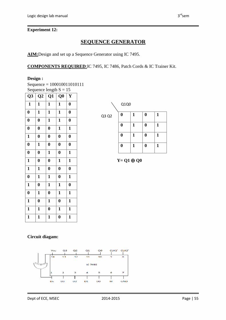
AIM:Design and set up a Sequence Generator using IC 7495. COMPONENTS REQUIRED:IC 7495, IC 7486, Patch Cords & IC Trainer Kit. Design : Sequence = 100010011010111 Sequence length S = 15
Y= Q1 ⨁ Q0
Circuit diagam:
Q3 Q2 Q1 Q0 Y
1 1 1 1 0
0 1 1 1 0
0 0 1 1 0
0 0 0 1 1
1 0 0 0 0
0 1 0 0 0
0 0 1 0 1
1 0 0 1 1
1 1 0 0 0
0 1 1 0 1
1 0 1 1 0
0 1 0 1 1
1 0 1 0 1
1 1 0 1 1
1 1 1 0 1
0 1 0 1
0 1 0 1
0 1 0 1
0 1 0 1
Q1Q0
Q3 Q2
Dept of ECE, MSEC 2014-2015 Page | 55
Logic design lab manual 3rdsem
PROCEDURE:
1. Check all the components for their working. 2. Insert the appropriate IC into the IC base. 3. Make connections as shown in the circuit diagram. 4. By Keeping mode=1. Load the input A,B,C,D as in Truth Table 1st Row and give a
clockpulse. 5. For count mode make mode = 0. 6. Verify the Truth Table and observe the outputs.
RESULT:
VIVA QUESTIONS: 1) What is the necessity for sequence generation?
2) What are PISO, SIPO, and SISO with respect to shift register?
3) Differentiate between serial data & parallel data