precise measurement of time duration separating two or several physical events. 3D scanners or 3D console games represent typical application requiring precise time quantification of the interval time to reconstitute a three-dimensional scene. Such systems are generally based on Time of Flight (TOF) measurement of the light emitted by a laser diode or a light-emitting diode (LED) and detected by a suitable light sensors after reflection by an object. The TOF of the light is proportional to the distance traveled by
the latter. The measurement is made independently by several pixels allowing the reconstitution of the 3D scene [1-2].
To measure this duration, we use devices capable of converting extremely low time durations (some tens of picoseconds) into digital values understandable for downstream processing and conditioning chain. These devices are commonly known as Time-to-Digital Converters (TDCs) [3]. The latter is largely used for several years in numerous smart sensor systems, particle and high-energy physics applications as well as measurement and instrumentation applications such as digital scopes and logic analyzers [3-4].
Sensors & Transducers, Vol. 193, Issue 10, October 2015, pp. 123-134
124
In order to design such systems there are several techniques which are proposed in literature. Some of the techniques that can be readily identified are [3, 5-6]: Tapped Delay Lines (TDL), Delay Locked Loop (DLL), Vernier Delay Line (VDL), Multilevel TDC, etc. All of these Time-to-Digital conversion techniques are usually designed as Application-Specific Integrated Circuits (ASICs) [7]. The latter have the advantage to have high performances but suffer from a higher cost, slow time to market and limited reconfiguration possibilities. It is also worth noting that the ASIC solutions are not suitable for integration into reconfigurable digital designs mostly described in Hardware Description Languages (HDL). As a result, numerous solutions for implementing TDCs on FPGA circuits have emerged [8-13]. However, the most significant limitation of these architectures is the difficulty to predict the placement and routing delays as well as the time delay of the logic gates itself. The consequence of this inevitable hardware restriction is a non-stable resolution of the designed TDC [10].
In this work, we aim to extend our contribution presented at SENSORCOMM 2015, consisting of introducing a design methodology for high resolution TDC on low cost FPGA targets [14] by including some improvements leading to new interesting results. This methodology enables the mastering of the network routing delays as well as the delays of the gates themselves. Therefore, it leads to an optimized TDC design with stable and accurate resolutions.
In order to give some background, the functional principle as well as the structure of the studied TDC in given in the second section. We also point out some associated difficulties encountered while using classical inverters as delay cells. The third section is dedicated to present our approach of implementing a TDC on an FPGA. Firstly, we show how to take advantage of the Carry Chain Logic to enhance and optimize TDC resolution. Secondly, we illustrate how to use the Chip Planner to define the exact physical layout location in the Chip. Therefore, we point out the importance of this operation. Section 4 provides a detailed case study consisting of implementing a 42 ps resolution TDC on Altera Cyclone IV low cost FPGA. The implemented TDC is associated to an FTDI (Future Technology Devices International) USB interface circuit operating in parallel mode with transfer rates reaching up to 40 Mbytes per second. Finally, we end our work by providing some final observations.
2. Setting in the Context
2.1. Functional Principle of the Studied TDC A TDC is an electronic system that measures the
interval time between two occurring events of a given signal. Its main purpose is to convert temporal
information to binary sequence understandable for a downstream processing chain.
For an accurate time duration measurement, generally, a TDC is composed of three blocks: two fine measurement blocks and a coarse one. The coarse one counts the number (N) of clock periods between enabling to disabling the measured interval, and the fine blocks evaluate the uncertainties in both sides that cannot be counted since their duration is shorter than the clock period.
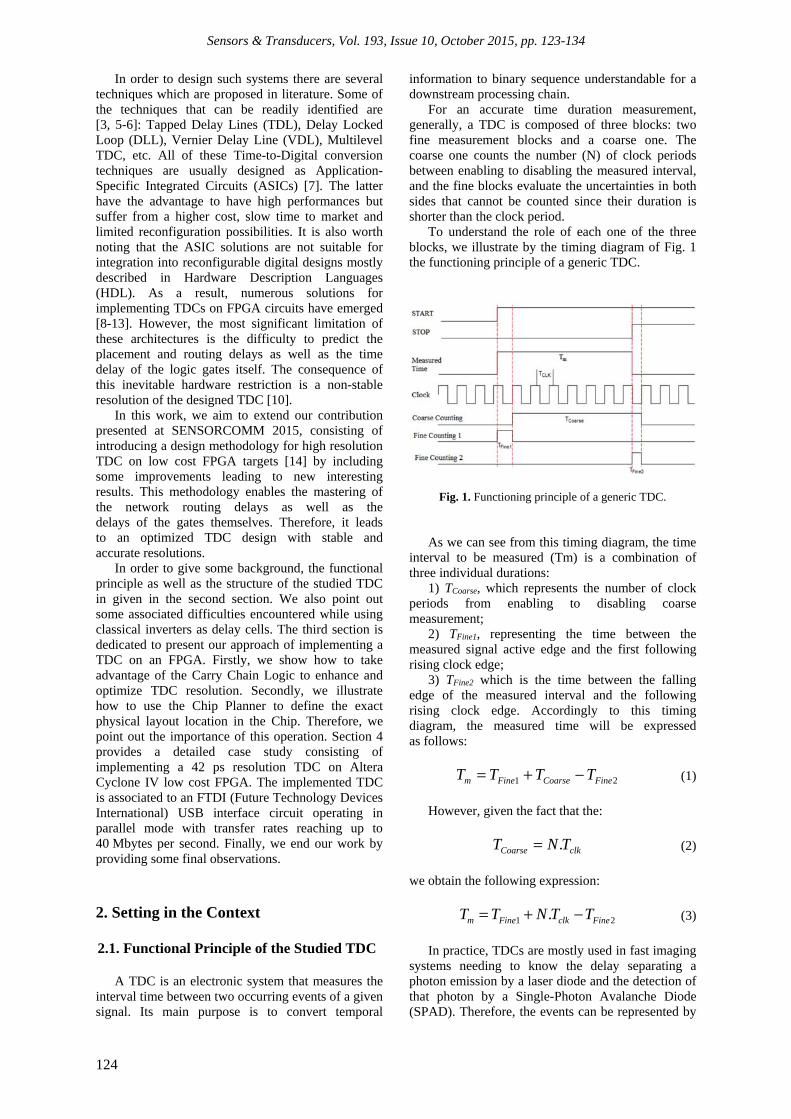
To understand the role of each one of the three blocks, we illustrate by the timing diagram of Fig. 1 the functioning principle of a generic TDC.
Fig. 1. Functioning principle of a generic TDC.
As we can see from this timing diagram, the time interval to be measured (Tm) is a combination of three individual durations:
1) TCoarse, which represents the number of clock periods from enabling to disabling coarse measurement;
2) TFine1, representing the time between the measured signal active edge and the first following rising clock edge;
3) TFine2 which is the time between the falling edge of the measured interval and the following rising clock edge. Accordingly to this timing diagram, the measured time will be expressed as follows:
21 FineCoarseFinem TTTT −+= (1)
However, given the fact that the:
clkCoarse TNT .= (2)
we obtain the following expression:
1 2.m Fine clk FineT T N T T= + − (3)
In practice, TDCs are mostly used in fast imaging
systems needing to know the delay separating a photon emission by a laser diode and the detection of that photon by a Single-Photon Avalanche Diode (SPAD). Therefore, the events can be represented by
Sensors & Transducers, Vol. 193, Issue 10, October 2015, pp. 123-134
125
two signals: (1) a START signal, which can be synchronized with the coarse counter clock, and (2) a STOP signal that means that the SPAD has detected a photon. In that case, the whole TDC can be reduced to a coarse counter associated to a fine TDC measuring TFine2. Consequently, the measured interval time will be given by the expression hereafter:
2.m clk FineT N T T= − (4)
Since the coarse block is a simple counter
incremented by the system clock, we will focus in the following section on the implementation of the fine TDC.
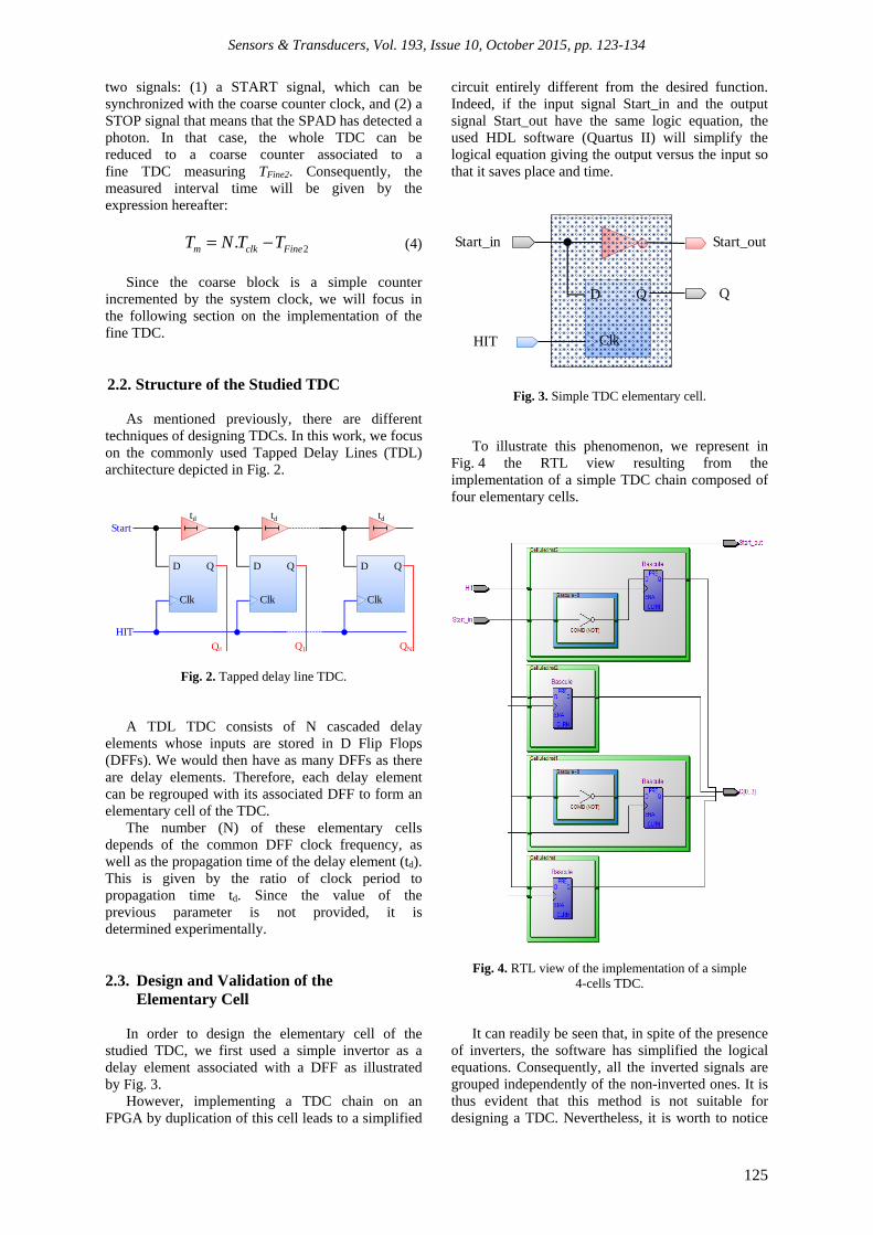
2.2. Structure of the Studied TDC As mentioned previously, there are different
techniques of designing TDCs. In this work, we focus on the commonly used Tapped Delay Lines (TDL) architecture depicted in Fig. 2.
D Q
Clk
D Q
Clk
D Q
Clk
Q0 Q1 QN
HIT
Starttd td td
Fig. 2. Tapped delay line TDC.
A TDL TDC consists of N cascaded delay elements whose inputs are stored in D Flip Flops (DFFs). We would then have as many DFFs as there are delay elements. Therefore, each delay element can be regrouped with its associated DFF to form an elementary cell of the TDC.
The number (N) of these elementary cells depends of the common DFF clock frequency, as well as the propagation time of the delay element (td). This is given by the ratio of clock period to propagation time td. Since the value of the previous parameter is not provided, it is determined experimentally.
2.3. Design and Validation of the Elementary Cell
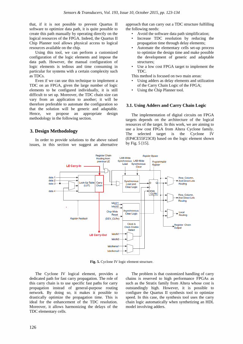
In order to design the elementary cell of the
studied TDC, we first used a simple invertor as a delay element associated with a DFF as illustrated by Fig. 3.
However, implementing a TDC chain on an FPGA by duplication of this cell leads to a simplified
circuit entirely different from the desired function. Indeed, if the input signal Start_in and the output signal Start_out have the same logic equation, the used HDL software (Quartus II) will simplify the logical equation giving the output versus the input so that it saves place and time.
D Q
Clk
Q
HIT
Start_in Start_out
Fig. 3. Simple TDC elementary cell.
To illustrate this phenomenon, we represent in Fig. 4 the RTL view resulting from the implementation of a simple TDC chain composed of four elementary cells.
Fig. 4. RTL view of the implementation of a simple 4-cells TDC.
It can readily be seen that, in spite of the presence of inverters, the software has simplified the logical equations. Consequently, all the inverted signals are grouped independently of the non-inverted ones. It is thus evident that this method is not suitable for designing a TDC. Nevertheless, it is worth to notice
Sensors & Transducers, Vol. 193, Issue 10, October 2015, pp. 123-134
126
that, if it is not possible to prevent Quartus II software to optimize data path, it is quite possible to create this path manually by operating directly on the logical resources of the FPGA. Indeed, the Quartus II Chip Planner tool allows physical access to logical resources available on the chip.
Using this tool, we can perform a customized configuration of the logic elements and impose the data path. However, the manual configuration of logic elements is tedious and time consuming in particular for systems with a certain complexity such as TDCs.
Even if we can use this technique to implement a TDC on an FPGA, given the large number of logic elements to be configured individually, it is still difficult to set up. Moreover, the TDC chain size can vary from an application to another; it will be therefore preferable to automate the configuration so that the solution will be generic and adaptable. Hence, we propose an appropriate design methodology in the following section.
3. Design Methodology
In order to provide solutions to the above raised issues, in this section we suggest an alternative
approach that can carry out a TDC structure fulfilling the following needs:
• Avoid the software data path simplification; • Increase TDC resolution by reducing the
propagation time through delay elements; • Automate the elementary cells set-up process
to optimize the design time and make possible the development of generic and adaptable structures;
• Use a low cost FPGA target to implement the TDC.
This method is focused on two main areas: • Using adders as delay elements and utilization
of the Carry Chain Logic of the FPGA; • Using the Chip Planner tool.
3.1. Using Adders and Carry Chain Logic The implementation of digital circuits on FPGA
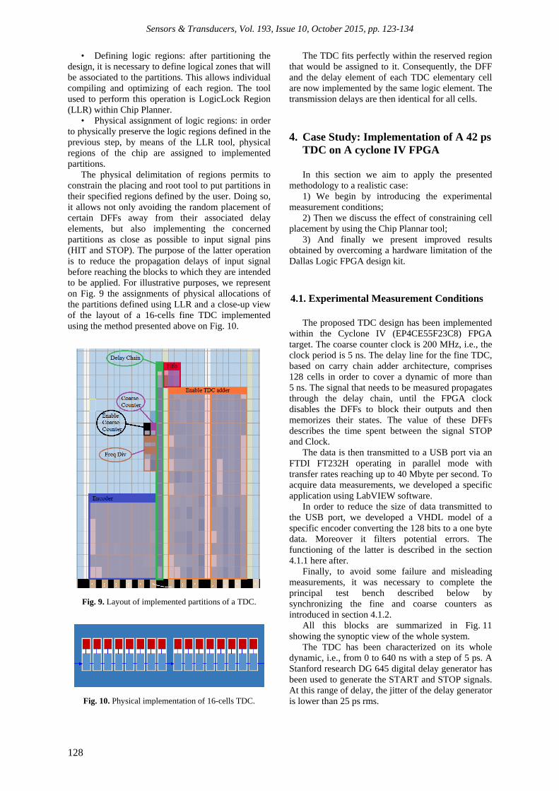
targets depends on the architecture of the logical resources of the target. In this work, we are aiming to use a low cost FPGA from Altera Cyclone family. The selected target is the Cyclone IV (EP4CE55F23C8) based on the logic element shown by Fig. 5 [15].
Fig. 5. Cyclone IV logic element structure.
The Cyclone IV logical element, provides a dedicated path for fast carry propagation. The role of this carry chain is to use specific fast paths for carry propagation instead of general-purpose routing network. By doing so, it makes it possible to drastically optimize the propagation time. This is ideal for the enhancement of the TDC resolution. Moreover, it allows harmonizing the delays of the TDC elementary cells.
The problem is that customized handling of carry chains is reserved to high performance FPGAs as such as the Stratix family from Altera whose cost is outstandingly high. However, it is possible to configure the Quartus II synthesis tool to optimize speed. In this case, the synthesis tool uses the carry chain logic automatically when synthetizing an HDL model involving adders.
Sensors & Transducers, Vol. 193, Issue 10, October 2015, pp. 123-134
127
It is therefore possible to use the carry chain logic to minimize and harmonize propagation delays for components involving adders. It is precisely the idea that is exploited here to design TDC elementary cells based on simple adders. This was done by developing a simple behavioral VHDL model for an adder with a customizable number of elementary cells. The number of the cells depends on the data width modeled by a generic parameter called DATA_WIDTH. The whole model is given by Fig. 6.
Fig. 6. Adder VHDL model.
The fine TDC using adders can be performed by: 1) Applying the TDC input signal STOP to the
carry input signal (cin) of the adder; 2) Choosing values for adder operand inputs
(a and b) so that an output carry is generated (cout=‘1’) if input carry is equal to ‘1’.
The output carry is then an exact replication of the input carry delayed by a transmission time through the cell. To do so, all it takes is to set all the bits of the first operand to ‘1’ and the bits of the second operand to ‘0’. For each bit (i) the arithmetic sum a(i)+b(i) gives ‘1’. When the input carry is activated (cin=‘1’) by the TDC input signal (STOP), the arithmetic sum a+b+cin gives ‘0’ and the carry output moves to ‘1’.
The Fig. 7 illustrates the implementation of one elementary cell of a TDC by a logic element of the Cyclone IV target. The adder cell is obtained by the look up table (LUT) and the DFF by the sequential configurable output register.
Theoretically, to obtain a TDC chain similar to the TDL structure shown by Fig. 2, it is sufficient to duplicate the structure of Fig. 7 as often as necessary to reach the number of desired cells. However, when implementing such a chain on the FPGA, some DFFs of the TDC elementary cells are dissociated of their corresponding 1-bit adder cells even if the data path is perfectly respected.
This phenomenon occurs randomly and leads to the placing of the DFF and the delay element of the
same TDC’s elementary cell in different logic elements, as shown in Fig. 8. The direct consequence of component misplacing is that the delay time is no longer identical for all cells. This inevitably generates unpredictable artifacts. To ensure a reliable operation, it is necessary to overcome this problem by constraining the placement tool to bring together the components of the same cell in the same logic element. This is the purpose of the next section.
Fig. 7. Implementation of a TDC elementary cell by a logic element.
Fig. 8. Random placing of DFFs on the chip.
3.2. Using Chip Planner Using a TDC in fast imaging systems requires the
measurement of very short time durations. It is therefore necessary to master all of the signal propagation delays through the cells as well as the routing network.
As we have seen in the previous section, unconstrained automatic implementation of a TDC on an FPGA usually leads to an inhomogeneous and irreproducible structure. Consequently, the measurement results are tainted by these uncertainties. Therefore, it is necessary to control the exact physical location of TDC cells on the chip.
This could be achieved by using the Chip Planner tool provided by Altera. The latter, according to the user's needs, allows the defining of specified implementation regions on the chip for blocks constituting the whole system. In addition, it supports incremental compilation to preserve the well-implemented parts and reduce the compilation time. This operation takes place in three distinct steps:
• Creating Design Partitions: the first step consists of dividing the design in individual partitions according to system complexity as well as user needs.
Sensors & Transducers, Vol. 193, Issue 10, October 2015, pp. 123-134
128
• Defining logic regions: after partitioning the design, it is necessary to define logical zones that will be associated to the partitions. This allows individual compiling and optimizing of each region. The tool used to perform this operation is LogicLock Region (LLR) within Chip Planner.
• Physical assignment of logic regions: in order to physically preserve the logic regions defined in the previous step, by means of the LLR tool, physical regions of the chip are assigned to implemented partitions.
The physical delimitation of regions permits to constrain the placing and root tool to put partitions in their specified regions defined by the user. Doing so, it allows not only avoiding the random placement of certain DFFs away from their associated delay elements, but also implementing the concerned partitions as close as possible to input signal pins (HIT and STOP). The purpose of the latter operation is to reduce the propagation delays of input signal before reaching the blocks to which they are intended to be applied. For illustrative purposes, we represent on Fig. 9 the assignments of physical allocations of the partitions defined using LLR and a close-up view of the layout of a 16-cells fine TDC implemented using the method presented above on Fig. 10.
Fig. 9. Layout of implemented partitions of a TDC.
Fig. 10. Physical implementation of 16-cells TDC.
The TDC fits perfectly within the reserved region that would be assigned to it. Consequently, the DFF and the delay element of each TDC elementary cell are now implemented by the same logic element. The transmission delays are then identical for all cells.
4. Case Study: Implementation of A 42 ps TDC on A cyclone IV FPGA In this section we aim to apply the presented
methodology to a realistic case: 1) We begin by introducing the experimental
measurement conditions; 2) Then we discuss the effect of constraining cell
placement by using the Chip Plannar tool; 3) And finally we present improved results
obtained by overcoming a hardware limitation of the Dallas Logic FPGA design kit.
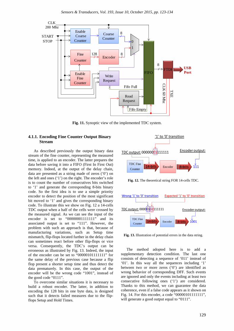
4.1. Experimental Measurement Conditions The proposed TDC design has been implemented
within the Cyclone IV (EP4CE55F23C8) FPGA target. The coarse counter clock is 200 MHz, i.e., the clock period is 5 ns. The delay line for the fine TDC, based on carry chain adder architecture, comprises 128 cells in order to cover a dynamic of more than 5 ns. The signal that needs to be measured propagates through the delay chain, until the FPGA clock disables the DFFs to block their outputs and then memorizes their states. The value of these DFFs describes the time spent between the signal STOP and Clock.
The data is then transmitted to a USB port via an FTDI FT232H operating in parallel mode with transfer rates reaching up to 40 Mbyte per second. To acquire data measurements, we developed a specific application using LabVIEW software.
In order to reduce the size of data transmitted to the USB port, we developed a VHDL model of a specific encoder converting the 128 bits to a one byte data. Moreover it filters potential errors. The functioning of the latter is described in the section 4.1.1 here after.
Finally, to avoid some failure and misleading measurements, it was necessary to complete the principal test bench described below by synchronizing the fine and coarse counters as introduced in section 4.1.2.
All this blocks are summarized in Fig. 11 showing the synoptic view of the whole system.
The TDC has been characterized on its whole dynamic, i.e., from 0 to 640 ns with a step of 5 ps. A Stanford research DG 645 digital delay generator has been used to generate the START and STOP signals. At this range of delay, the jitter of the delay generator is lower than 25 ps rms.
Sensors & Transducers, Vol. 193, Issue 10, October 2015, pp. 123-134
129
8
8
8128
EnableFine
Counter
Fine
Counter
CoarseCounter
FIFO
Encoder
FTDI
EnableCoarse
Counter 0
1
WriteRequest
ReadRequest
CLK 200 Mhz
STARTSTOP
USBPort
CL
K 60 M
hz
TX
E
Fifo Empty
Fifo Full
Fig. 11. Synoptic view of the implemented TDC system.
4.1.1. Encoding Fine Counter Output Binary
Stream As described previously the output binary data
stream of the fine counter, representing the measured time, is applied to an encoder. The latter prepares the data before saving it into a FIFO (First In First Out) memory. Indeed, at the output of the delay chain, data are presented as a string made of zeros (‘0’) on the left and ones (‘1’) on the right. The encoder’s role is to count the number of consecutives bits switched to ‘1’ and generate the corresponding 8-bits binary code. So the first idea is to use a simple priority encoder to detect the position of the most significant bit moved to ‘1’ and gives the corresponding binary code. To illustrate this we show on Fig. 12 a 14-cells TDC output when a half of the cells were crossed by the measured signal. As we can see the input of the encoder is set to “00000001111111” and its associated output is set to “111”. However, the problem with such an approach is that, because of manufacturing variations, such as Setup time mismatch, flip-flops located further in the delay chain can sometimes react before other flip-flops or vice versa. Consequently, the TDC’s output can be erroneous as illustrated by Fig. 13. Indeed, the input of the encoder can be set to “00000101111111” for the same delay of the previous case because a flip flop present a shorter setup time and thus detect the data prematurely. In this case, the output of the encoder will be the wrong code “1001”, instead of the good code “0111”.
To overcome similar situations it is necessary to build a robust encoder. The latter, in addition to encoding the 128 bits in one byte data, is designed such that it detects failed measures due to the flip-flops Setup and Hold Times.
TDC Fine
CounterEncoder14-bits
TDC output: 00000001111111
1118-bits
‘1’ to ‘0’ transition
Encoder output:
Fig. 12. The theoretical string FOR 14-cells TDC.
TDC Fine
CounterEncoder14-bits
TDC output: 00000101111111
10018-bits
Expected ‘1’ to ‘0’ transition
Encoder output:
Wrong ‘1’ to ‘0’ transition
Fig. 13. Illustration of potential errors in the data string.
The method adopted here is to add a supplementary detection condition. The last one consists of detecting a sequence of ‘011’ instead of ‘01’. In this way all the sequences including ‘1’ between two or more zeros (‘0’) are identified as wrong behavior of corresponding DFF. Such events are ignored and only the events including at least two consecutive following ones (‘1’) are considered. Thanks to this method, we can guarantee the data coherence, even if a false code appears as it shown on Fig. 14. For this encoder, a code “00000101111111”, will generate a good output equal to “0111”.
Sensors & Transducers, Vol. 193, Issue 10, October 2015, pp. 123-134
130
TDC Fine
CounterEncoder14-bits
TDC output: 00000101111111
1118-bits
Validated ‘11’ to ‘0’ transition
Encoder output:
Ignored ‘1’ to ‘0’ transition
Fig. 14. Correction of potential errors by the encoder.
4.1.2. Synchronization of Fine and Coarse Counters
The last step in the process is the synchronization
of the Fine and the Coarse counter. Without this step, measure noise could promptly be equal to the least significant bit of the coarse counter during its state changes.
To prevent this problem, a second clock is instantiated. Its operating frequency is the same as the main clock in the circuit, except its phase will be slightly shifted.
One of the two clock rate the coarse counter and the other one rate the fine counter. By changing the second clock phase, it is possible to perfectly synchronize the fine and coarse counter.
4.2. Effect of Constraining Cell Placement by the Chip Planer Tool
To show the effect of constraining cell placement
by the Chip Planer tool we report on Fig. 15 the detail of the unconstrained and constrained fine TDC measurements between two reference clock edges, i.e., on a range of 5 ns.
1500 2000 2500 3000 3500 4000 4500 5000 5500 6000
0
20
40
60
80
100
120
Time (ps)
Fin
e TD
C R
AW
data (lsb)
y = 0.0241*x - 34.1
Unconstrainted TDC raw data
Constrainted TDC raw data
linear fit
Fig. 15. Responses of Fine unconstrained and constrained TDC.
The unconstrained fine TDC response (blue) shows a large discrepancy of the LSB value indicating that some DFFs have been randomly placed. The resulting large steps make the unconstrained fine TDC unusable for sub nanosecond timing. Consequently, the use of the Chip Planner tool as described in section III is mandatory to obtain the behavior of the constrained fine TDC represented by the green curve. A linear fit is then used to assess the LSB value of the fine TDC which is given by the inverse of the linear fit slope, i.e., 41.5 ps in this study case.
4.3. Jitter, INL and DNL Evaluation
The noise visible on the fine TDC response, depicted on Fig. 15 bellow, is due to the jitter. The latter adds uncertainty on each measurement and it can be evaluated by computing the standard deviation
of a set of measurements at a given fixed delay between the START and STOP signals.
The jitter depicted in Fig. 16 has been characterized for different delays corresponding to a given signal propagation along the fine TDC line. As each fine TDC elementary cell adds its own jitter [16], the global jitter will then increase as a square root of the number N cells as given by the following expression:
2 2 Nα β+ ⋅ , (5)
where α is the initial jitter present at the input of the first cell and β the single cell jitter.
A curve, following this law is fitted on the jitter profile to underline the jitter’s variation relationship in the delay line. The extraction of this parameters leads to an initial jitter α of 62 ps rms and a single cell jitter β of 5.8 ps rms.
Sensors & Transducers, Vol. 193, Issue 10, October 2015, pp. 123-134
131
The accumulated jitter across the fine TDC delay line leads to a mean jitter of 90 ps rms. Thus, the line length has to be kept as low as possible in order to obtain the best accuracy. This can be done by using the fastest achievable frequency for the coarse counter.
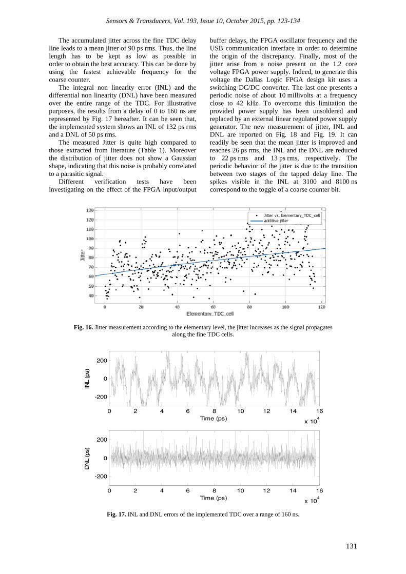
The integral non linearity error (INL) and the differential non linearity (DNL) have been measured over the entire range of the TDC. For illustrative purposes, the results from a delay of 0 to 160 ns are represented by Fig. 17 hereafter. It can be seen that, the implemented system shows an INL of 132 ps rms and a DNL of 50 ps rms.
The measured Jitter is quite high compared to those extracted from literature (Table 1). Moreover the distribution of jitter does not show a Gaussian shape, indicating that this noise is probably correlated to a parasitic signal.
Different verification tests have been investigating on the effect of the FPGA input/output
buffer delays, the FPGA oscillator frequency and the USB communication interface in order to determine the origin of the discrepancy. Finally, most of the jitter arise from a noise present on the 1.2 core voltage FPGA power supply. Indeed, to generate this voltage the Dallas Logic FPGA design kit uses a switching DC/DC converter. The last one presents a periodic noise of about 10 millivolts at a frequency close to 42 kHz. To overcome this limitation the provided power supply has been unsoldered and replaced by an external linear regulated power supply generator. The new measurement of jitter, INL and DNL are reported on Fig. 18 and Fig. 19. It can readily be seen that the mean jitter is improved and reaches 26 ps rms, the INL and the DNL are reduced to 22 ps rms and 13 ps rms, respectively. The periodic behavior of the jitter is due to the transition between two stages of the tapped delay line. The spikes visible in the INL at 3100 and 8100 ns correspond to the toggle of a coarse counter bit.
Fig. 16. Jitter measurement according to the elementary level, the jitter increases as the signal propagates along the fine TDC cells.
0 2 4 6 8 10 12 14 16
x 10
4
-200
0
200
Time (ps)
IN
L (ps)
0 2 4 6 8 10 12 14 16
x 10
4
-200
0
200
Time (ps)
DN
L (ps)
Fig. 17. INL and DNL errors of the implemented TDC over a range of 160 ns.
Sensors & Transducers, Vol. 193, Issue 10, October 2015, pp. 123-134
132
Table 1. Comparison of recent implementations of TDC on different FPGA targets.
Reference Date Architecture FPGA Resolution Jitter DNL INL
Fig. 18. New Jitter measurement after replacing the Dallas Logic power supply core by a DC regulated power supply.
0 1000 2000 3000 4000 5000 6000 7000 8000
-100
-50
0
50
100
Time (ps)
INL (ps)
0 1000 2000 3000 4000 5000 6000 7000 8000
-20
-10
0
10
20
Time (ps)
DNL (ps)
Fig. 19. New INL and DNL errors of the implemented TDC over a range of 160 ns after disabling the Dallas Logic supply core.
Sensors & Transducers, Vol. 193, Issue 10, October 2015, pp. 123-134
133
5. Conclusions
This paper has proposed a global methodology to design and implement Time-to-Digital Converters on low cost FPGA targets. It presents how to use different tools to enhance the TDC resolution by reducing propagation delays through the connection network as well as the logic gates themselves. First, the use of adders as delay elements, to benefit from a dedicated carry chain logic path, is presented. Then we detailed how to take advantage of the chip planner, to constrain the placing and root tool to put the partitions of the system in user specified physical regions. Doing so, it allowed the mastering of propagation delays and consequently improved the resolution and the stability of the TDC.
The work is ended by a case study that applied this methodology to design a TDC with a resolution of about 42 ps on a Cyclone IV FPGA. The implemented TDC presents a jitter of only 26 ps rms, and the DNL and the INL has been measured respectively to 22 and 13 ps rms. As we can see from the state of the art summarized in Table 1, comparable values of our results are obtained but by using high performances FPGA targets as such as Virtex 6 of Xilinx which are highly expensive.
The highlighted results in this paper are very promising, not only because they are suitable for domains requiring high performances, but also because they are achieved by using a low cost FPGA family which opens the door to a broader use in a great amount of fast application fields.
As a perspective in the near future, we plan to integrate the presented TDC in different applications such as image photon counting devices and microfluidic experimentations [17].
References [1]. L. Li, Time-of-flight camera – an introduction, Texas
Instruments, SLOA190B – Technical White Paper, January 2014, revised May 2014.
[2]. E. Charbon, M. Fishburn, R. Walker, R. K. Henderson, C. Niclass, SPAD-based sensors TOF Range-Imaging Cameras, F. Remondino and D. Stoppa (Eds.), Springer-Verlag, Berlin Heidelberg, 2013, pp. 11-38.
[3]. S. Henzler, Time-to-Digital Converters, Springer Science+Business Media B. V., 2010.
[4]. S. Y. Yurish, Smart Optoelectronic Sensors and Intelligent Sensor Systems, Sensors & Transducers, Vol. 14-1, Special Issue, March 2012, pp. 18-31.
[5]. J. Kalisz, Review of methods for time interval measurements with picoseconds resolution, Metrologia, Vol. 41, No. 1, 2004, pp. 17-32.
[6]. C. S. Hwang, P. Chen, H. W. Tsao, A high-precision Time-to-Digital converter using a two-level conversion scheme, IEEE Transactions on Nuclear Science, Vol. 51, No. 4, 2004, pp. 1349-1352.
[7]. I. Malasse, W. Uhring, J. Le Normand, N. Dumas, F. Dadouche, 10-ps Resolution Hybrid Time to Digital Converter in a 0.18 µm CMOS Technology,
in Proceedings of the IEEE 12th International New Circuits and Systems Conference (NEWCAS), June 2014, pp. 105-108.
[8]. J. Kalisz, R. Szplet, J. Pasierbinski, A. Poniecki, Field-programmable-gate-array-based time-to-digital converter with 200-ps resolution, IEEE Transactions on Instrumentation and Measurement, Vol. 46, Issue 1, 1997, pp. 51-55.
[9]. I. Vornicu, R. Carmona-Galán, Á. Rodríguez-Vázquez, Wide range 8-ps incremental resolution time interval generator based on FPGA technology, in Proceedings of the IEEE 21st International Conference on Electronics, Circuits and Systems (ICECS’14), 2014, pp. 395-398.
[10]. M. Lin, G. Tsai, C. Liu, S. Chu, FPGA-Based high area efficient Time-to-Digital IP design, in Proceedings of the IEEE Region 10 Conference (TENCON’06), 2006, pp. l-4.
[11]. R. Narasimman, A. Prabhakar, N. Chandrachoodan, Implementation of a 30 ps resolution Time-to-Digital Converter in FPGA, in Proceedings of the IEEE International Conference on EDCAV, 2015, pp. 12-17.
[12]. A. Aloisio, P. Branchini, R. Giordano, V. Izzo, S. Loffredo, High-precision Time-to-Digital converter in a FPGA device, in Proceedings of the IEEE Nuclear Science Symposium Conference Record (NSS/MIC), Vol. 13, 2009, pp. 290-294.
[13]. S. S. Junnarkar, P. O’Connor, R. Fontaine, FPGA based self calibrating 40 picosecond resolution, wide range Time-to-Digital converter, in Proceedings of the IEEE Nuclear Science Symposium Conference Record (NSS '08), 2008, pp. 3434-3439.
[14]. F. Dadouche, T. Turko, W. Uhring, I. Malass, J. Bartringer, J.-P. Le Normand, Design Methodology of TDC on Low Cost FPGA Targets, in Proceedings of the 9th International Conference on Sensor Technologies and Applications (SENSORCOMM’ 2015), Venice, Italy, 23-27 August 2015, pp. 29-34.
[15]. Cyclone IV Device Handbook, Vol. 1, Chapter 2, Altera Corporation, April 2014.
[16]. M. Zlatanski, W. Uhring, J.-P. Le Normand, D. Mathiot, A Fully characterizable asynchronous multiphase delay generator, IEEE Transactions on Nuclear Science, Vol. 58, No. 2, 2011, pp. 418-425.
[17]. J. Léonard, N. Dumas, J. Causse, S. Maillot, N. Giannakopoulou, S. Barre, W. Uhring, High-throughput time-correlated single photon counting, Lab on a Chip - Royal Society of Chemistry, Vol. 14, No. 22, November 2014, pp. 4338-4343.
[18]. H. Menninga, C. Favi, M. W. Fishburn, E. Charbon, A multi-channel, 10ps resolution, FPGA-based TDC with 300MS/s throughput for open-source PET applications, in Proceedings of the IEEE Nuclear Science Symposium and Medical Imaging Conference (NSS/MIC), 23-29 Oct. 2011, pp. 1515-1522.
[19]. J. Y. Won, S. I. Kwon, H. S. Yoon, G. B. Ko, J.-W. Son, J. S. Lee, Dual-Phase Tapped-Delay-Line Time-to-Digital Converter with On-the-Fly Calibration Implemented in 40 nm FPGA, IEEE Transactions on Biomedical Circuits and Systems, Vol. PP, No. 99, p. 1.
[20]. L. Arpin, M. Bergeron, M-A.Tetrault, R. Lecomte, R. Fontaine, A Sub-Nanosecond Time Interval Detection System Using FPGA Embedded I/O Resources, IEEE Transactions on Nuclear Science, Vol. 57, No. 2, April 2010, pp. 519-524.
[21]. J. Song, Q. An, S. Liu, A high-resolution time-to-digital converter implemented in field-
Sensors & Transducers, Vol. 193, Issue 10, October 2015, pp. 123-134
134
programmable-gate-arrays, IEEE Transactions on Nuclear Science, Vol. 53, No. 1, February 2006, pp. 236-241.
[22]. L. Zhao, X. Hu, S. Liu, J. Wang, Q. An, A 16-channel 15 ps TDC implemented in a 65 nm FPGA, in Proceedings of the 18th IEEE-NPSS Real Time Conference (RT), 9-15 June 2012, pp. 1-5.
[23]. M. Daigneault, J.-P. David, A novel 10 ps resolution TDC architecture implemented in a 130 nm process FPGA, in Proceedings of the 8th IEEE International NEWCAS Conference (NEWCAS), 20-23 June 2010, pp. 281-284.