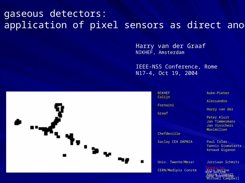
New gaseous detectors: the application of pixel sensors as direct anode. Harry van der Graaf NIKHEF, Amsterdam IEEE-NSS Conference, Rome N17-4, Oct 19, 2004. NIKHEFAuke-Pieter Colijn Alessandro Fornaini Harry van der Graaf Peter Kluit Jan Timmermans Jan Visschers - PowerPoint PPT Presentation
gaseous detectors: application of pixel sensors as direct anod NIKHEF Auke-Pieter Colijn Alessandro Fornaini Harry van der Graaf Peter Kluit Jan Timmermans Jan Visschers Maximilien Chefdeville Saclay CEA DAPNIA Paul Colas Yannis Giomataris Arnaud Giganon Univ. Twente/Mesa+ Jurriaan Schmitz CERN/Medipix Constm Eric Heijne Xavie Llopart Michael Campbell Thanks to: Wim Gotink Joop Rovenkamp Harry van der Graaf NIKHEF, Amsterdam IEEE-NSS Conference, Rome N17-4, Oct 19, 2004
Transcript
New gaseous detectors:the application of pixel sensors as direct anode
NIKHEF Auke-Pieter ColijnAlessandro FornainiHarry van der GraafPeter KluitJan TimmermansJan VisschersMaximilien
Chefdeville
Saclay CEA DAPNIA Paul ColasYannis GiomatarisArnaud Giganon
Univ. Twente/Mesa+ Jurriaan Schmitz
CERN/Medipix Constm Eric HeijneXavie LlopartMichael CampbellThanks to:
Wim GotinkJoop Rovenkamp
Harry van der GraafNIKHEF, Amsterdam
IEEE-NSS Conference, RomeN17-4, Oct 19, 2004
Original motivation:
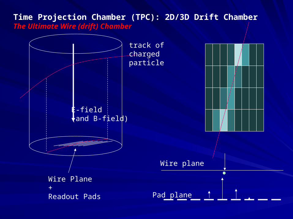
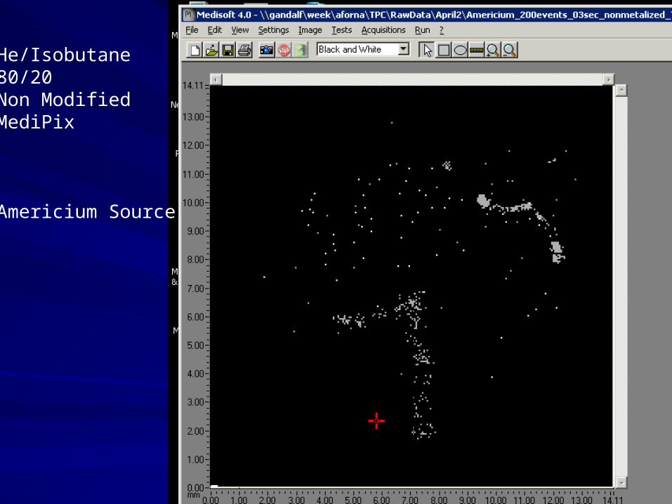
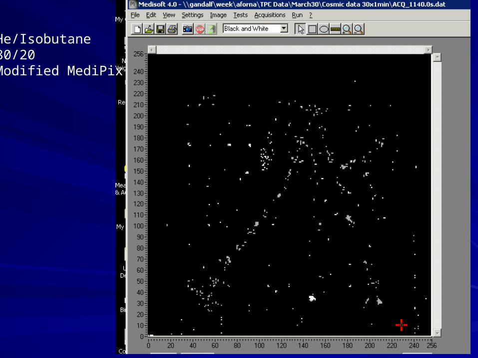
Si pixel readout for the Time Projection Chamber (TPC)
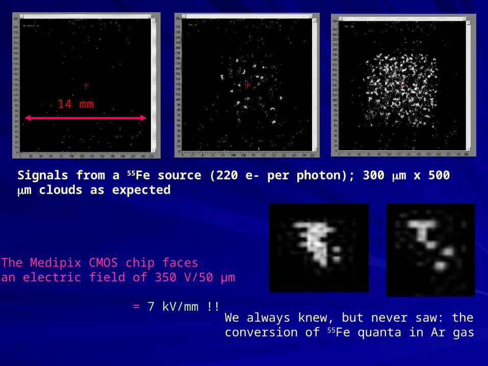
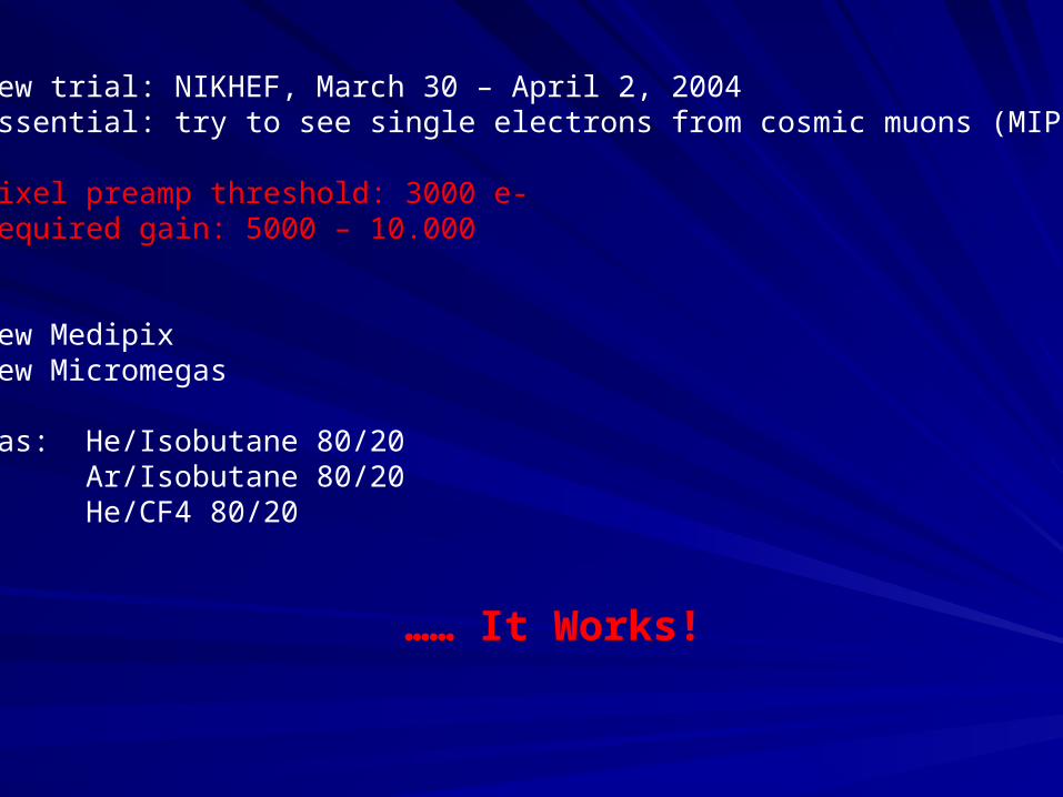
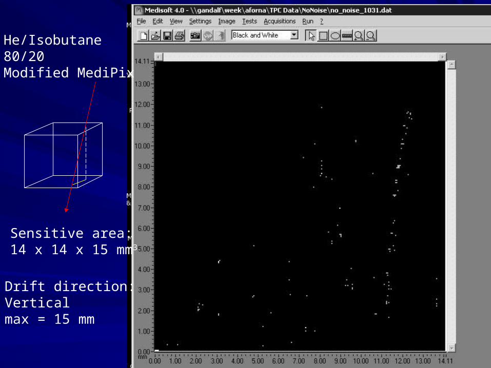
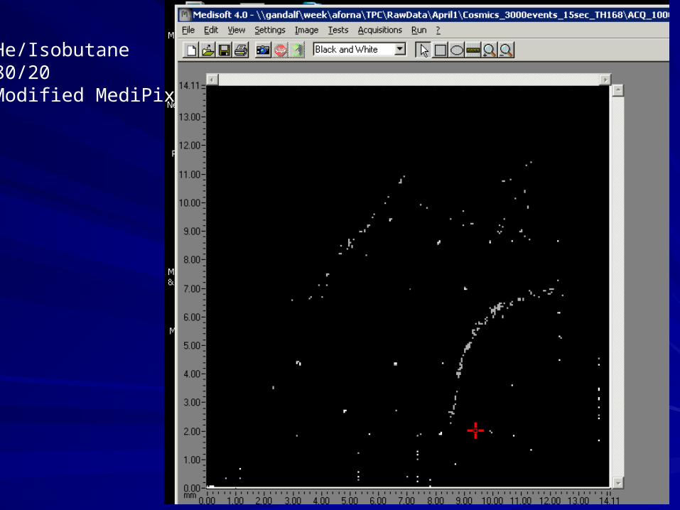
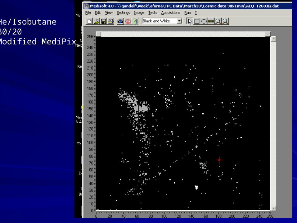
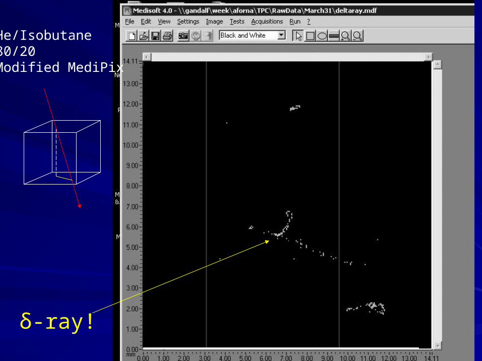
• We can reach very high gas gains with He-based gases (> 100k!)• The MedPix2 chip can withstand strong E-fields (10 kV/mm!)• Discharges ruin the chip immediately (broke 4 in 4 days!)• Measured efficiency: > 0.9; consistent with high gain• Seen MIPs, clusters, δ-rays, electrons, α ‘s……
- Development of TimePix 1: TDC per pixel instead of counter
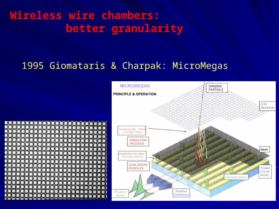
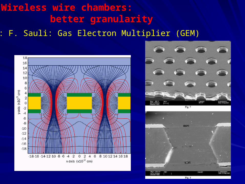
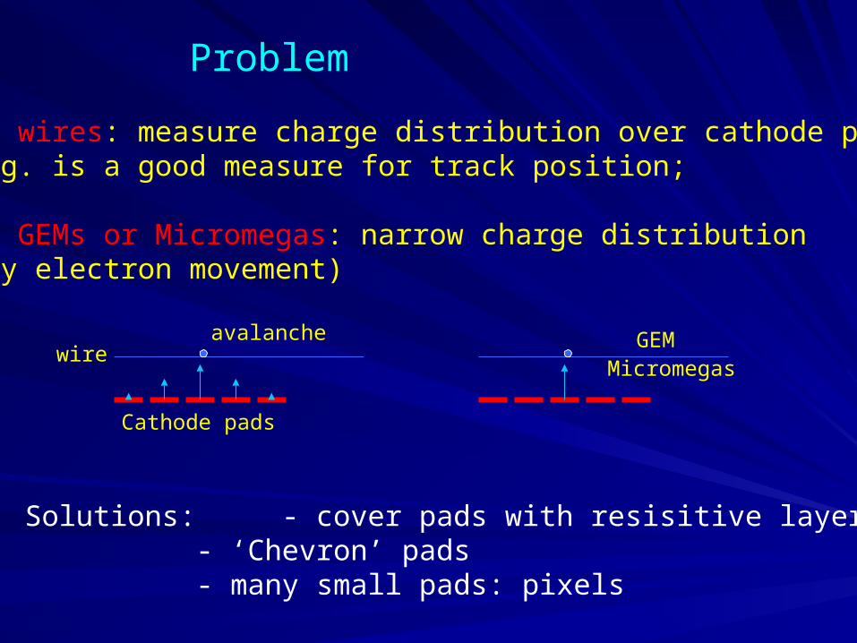
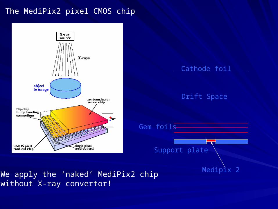
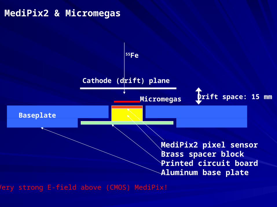
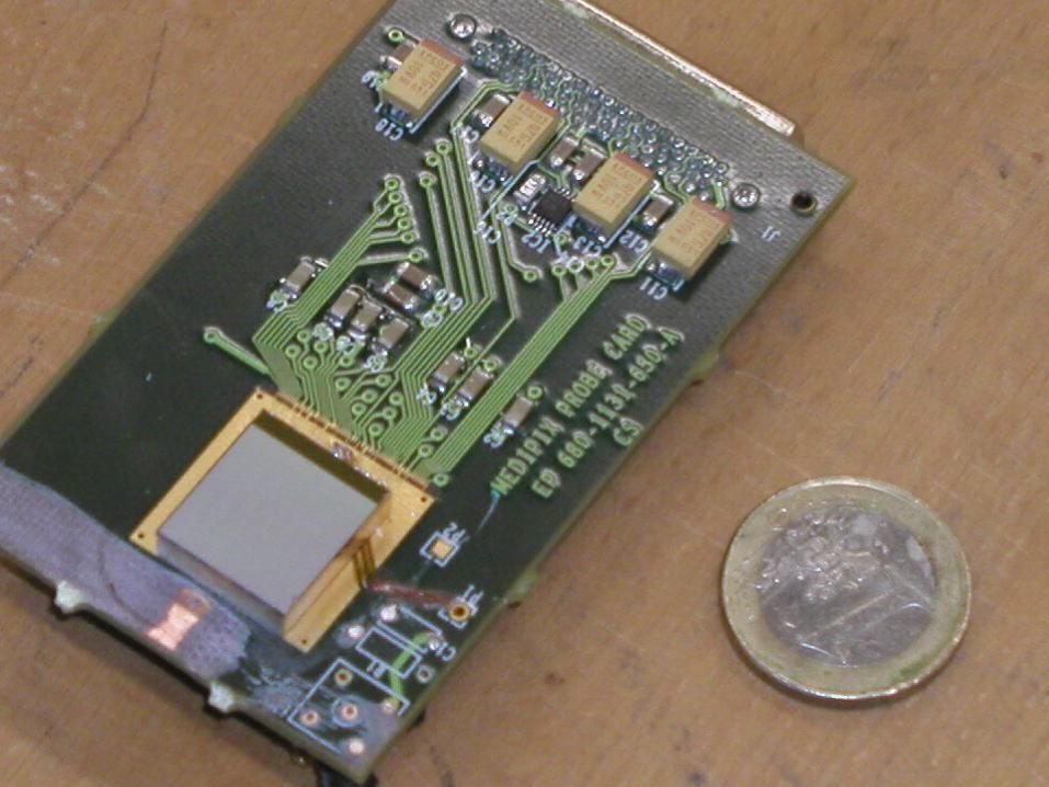
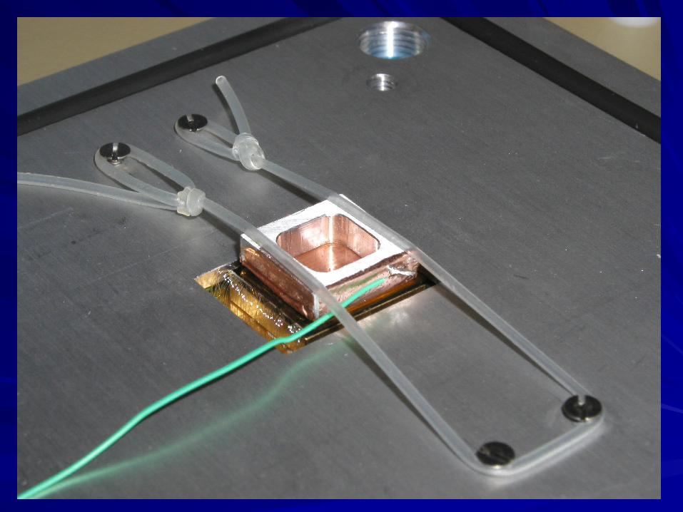
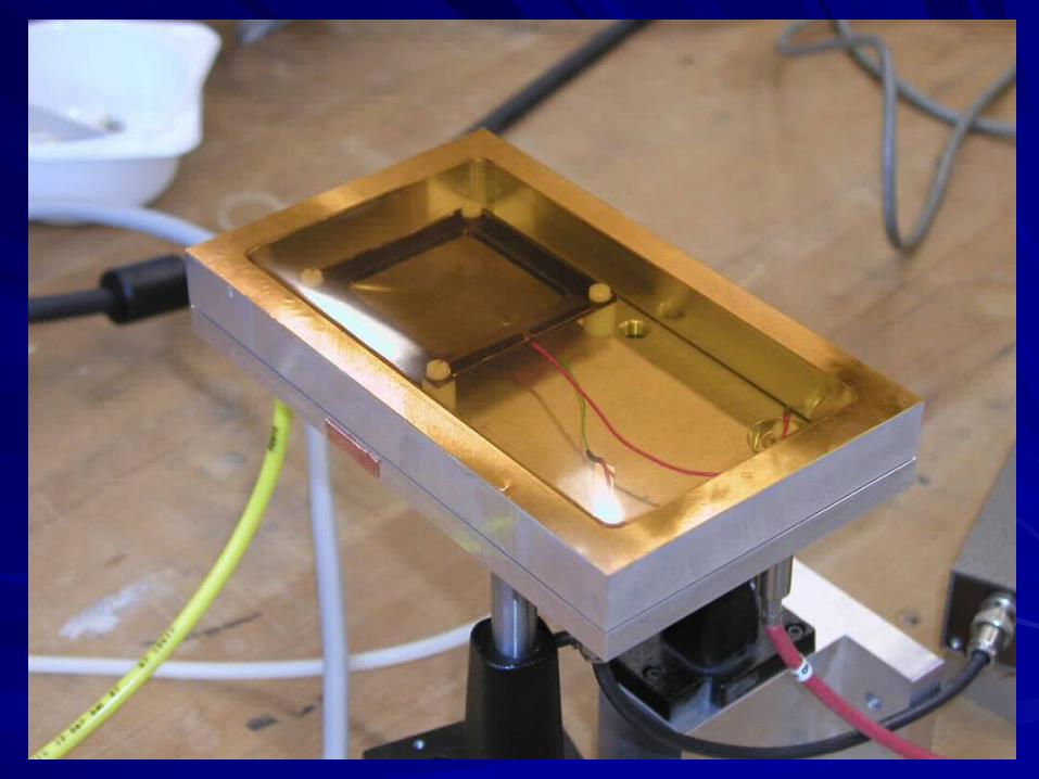
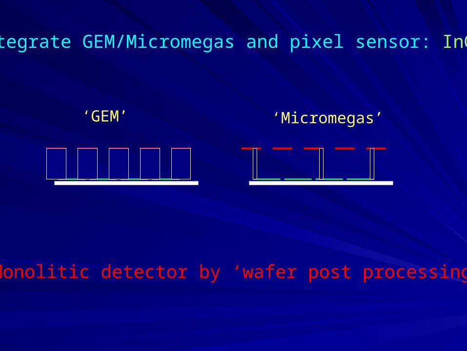
Integrate GEM/Micromegas and pixel sensor: InGrid
‘GEM’ ‘Micromegas’
Monolitic detector by ‘wafer post processing’
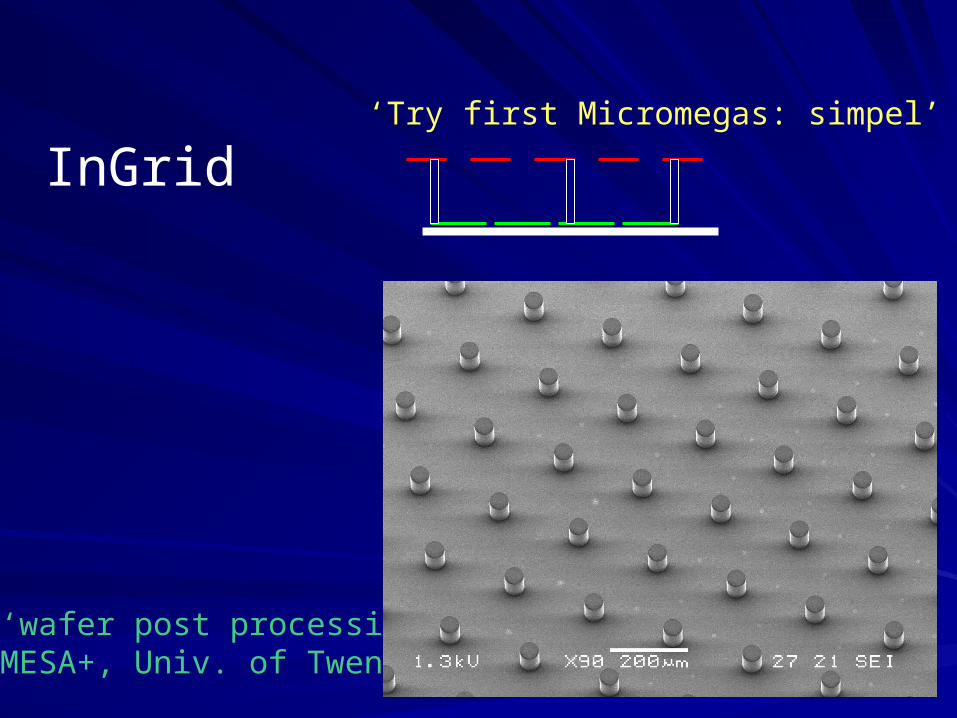
‘Try first Micromegas: simpel’
By ‘wafer post processing’at MESA+, Univ. of Twente
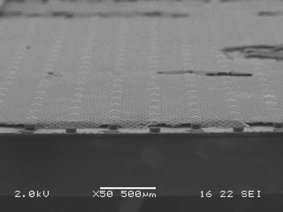
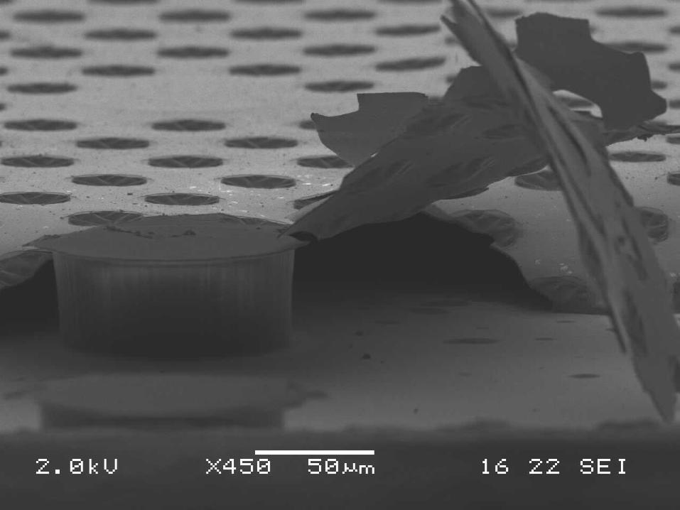
InGrid
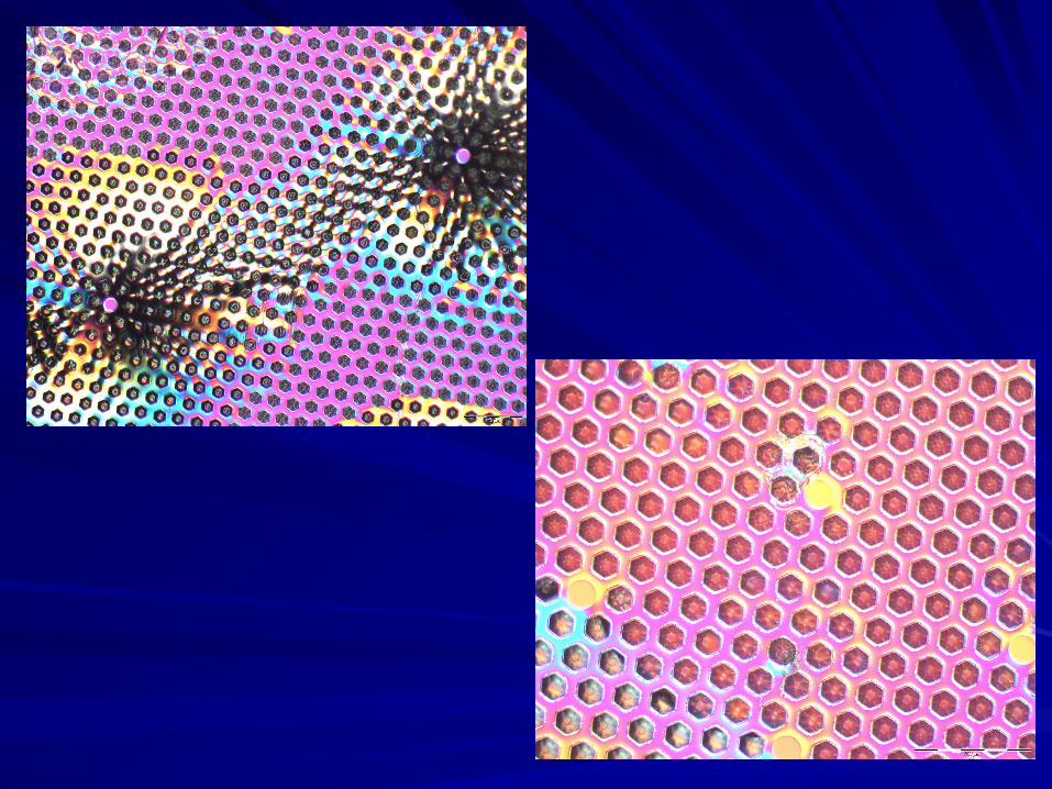
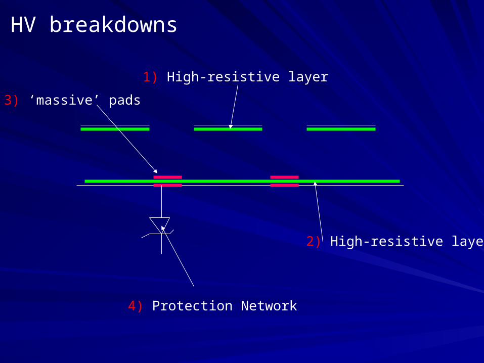
HV breakdowns
4) Protection Network
1) High-resistive layer
2) High-resistive layer
3) ‘massive’ pads
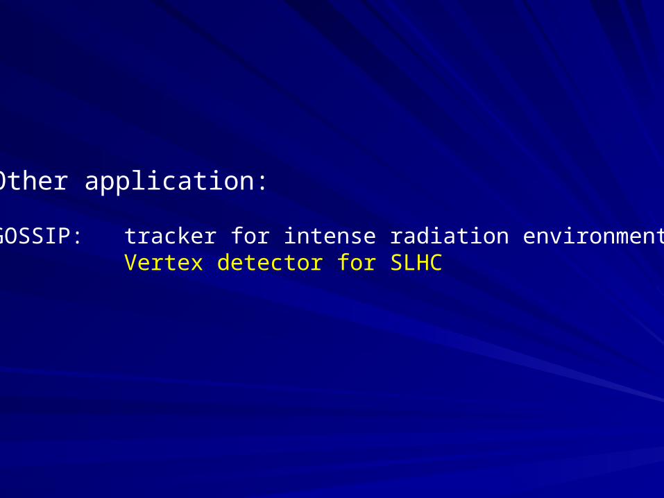
Other application:
GOSSIP: tracker for intense radiation environment:Vertex detector for SLHC
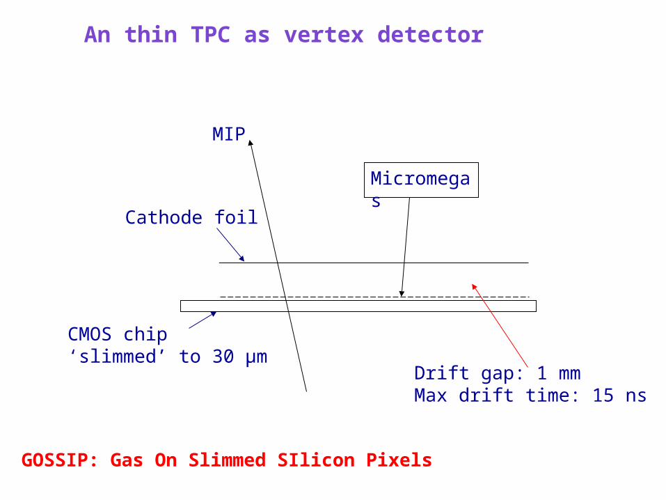
GOSSIP: Gas On Slimmed SIlicon Pixels
CMOS pixel array
MIP
Micromegas
Drift gap: 1 mmMax drift time: 15 ns
MIP
CMOS chip‘slimmed’ to 30 μm
Cathode foil
An thin TPC as vertex detector
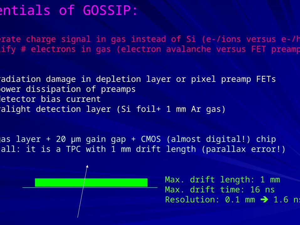
Essentials of GOSSIP:
• Generate charge signal in gas instead of Si (e-/ions versus e-/holes)• Amplify # electrons in gas (electron avalanche versus FET preamps)
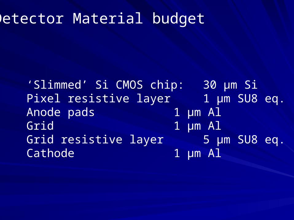
Then:• No radiation damage in depletion layer or pixel preamp FETs• No power dissipation of preamps• No detector bias current• Ultralight detection layer (Si foil+ 1 mm Ar gas)
1 mm gas layer + 20 μm gain gap + CMOS (almost digital!) chipAfter all: it is a TPC with 1 mm drift length (parallax error!)
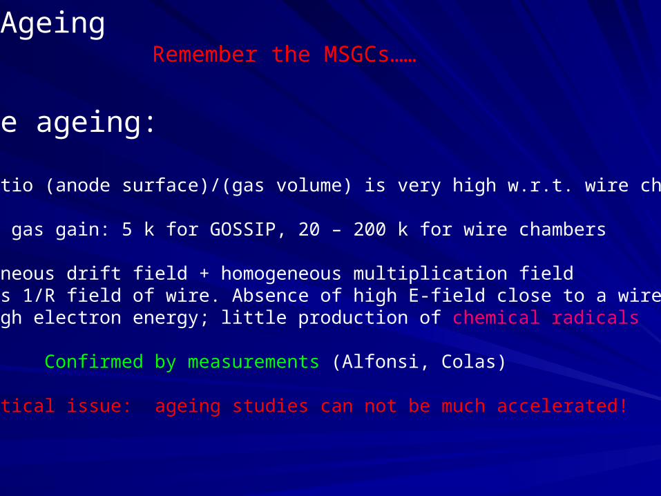
• the ratio (anode surface)/(gas volume) is very high w.r.t. wire chambers
• little gas gain: 5 k for GOSSIP, 20 – 200 k for wire chambers
• homogeneous drift field + homogeneous multiplication field versus 1/R field of wire. Absence of high E-field close to a wire: no high electron energy; little production of chemical radicals
Confirmed by measurements (Alfonsi, Colas)
But: critical issue: ageing studies can not be much accelerated!
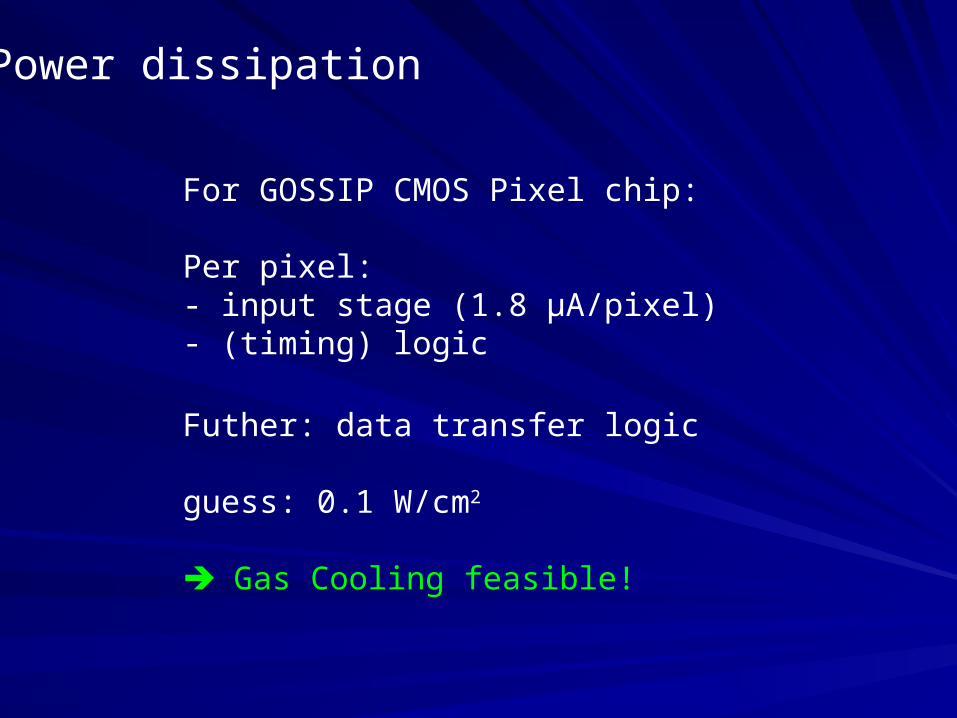
Power dissipation
For GOSSIP CMOS Pixel chip:
Per pixel: - input stage (1.8 μA/pixel)- (timing) logic
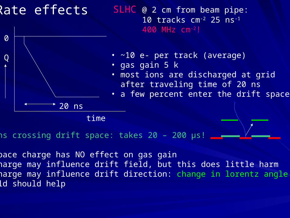
• ~10 e- per track (average)• gas gain 5 k• most ions are discharged at grid after traveling time of 20 ns• a few percent enter the drift space:
SLHC @ 2 cm from beam pipe:10 tracks cm-2 25 ns-1
400 MHz cm-2!
Some ions crossing drift space: takes 20 – 200 μs!
• ion space charge has NO effect on gas gain• ion charge may influence drift field, but this does little harm• ion charge may influence drift direction: change in lorentz angle ~0.1 rad• B-field should help
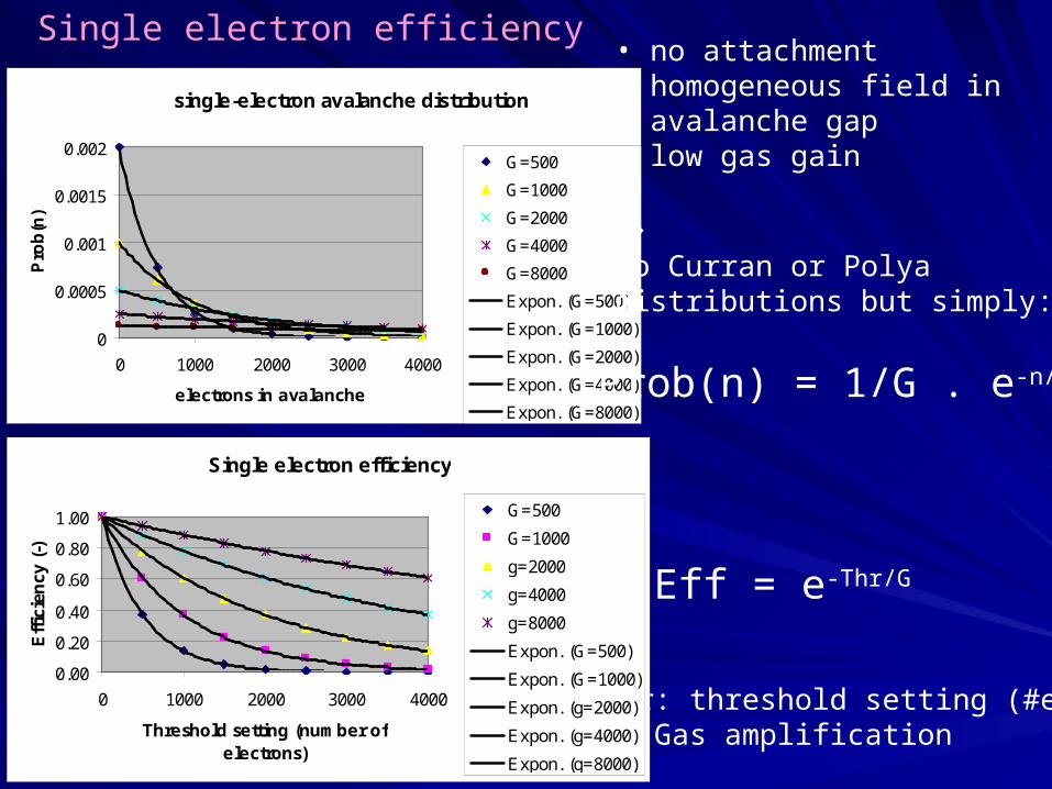
Efficiency
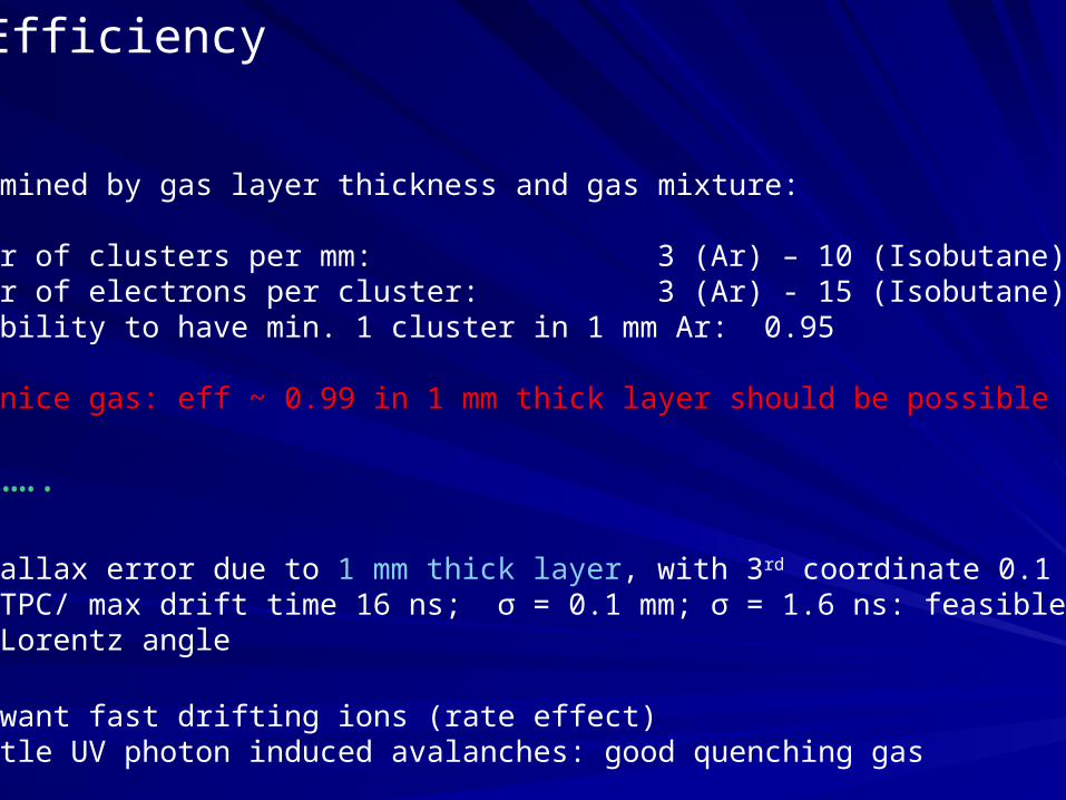
Determined by gas layer thickness and gas mixture:
Number of clusters per mm: 3 (Ar) – 10 (Isobutane)Number of electrons per cluster: 3 (Ar) - 15 (Isobutane)Probability to have min. 1 cluster in 1 mm Ar: 0.95
With nice gas: eff ~ 0.99 in 1 mm thick layer should be possible
But…….
• Parallax error due to 1 mm thick layer, with 3rd coordinate 0.1 mm:• TPC/ max drift time 16 ns; σ = 0.1 mm; σ = 1.6 ns: feasible!• Lorentz angle
• We want fast drifting ions (rate effect)• little UV photon induced avalanches: good quenching gas
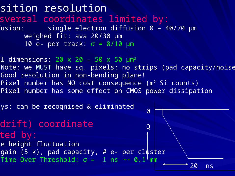
Position resolutionTransversal coordinates limited by:• Diffusion: single electron diffusion 0 – 40/70 µm
weighed fit: ava 20/30 µm10 e- per track: σ = 8/10 µm
• pixel dimensions: 20 x 20 – 50 x 50 μm2 Note: we MUST have sq. pixels: no strips (pad capacity/noise)Good resolution in non-bending plane!Pixel number has NO cost consequence (m2 Si counts)Pixel number has some effect on CMOS power dissipation
• δ-rays: can be recognised & eliminated
3rd (drift) coordinatelimited by:• Pulse height fluctuation• gas gain (5 k), pad capacity, # e- per cluster With Time Over Threshold: σ = 1 ns ~~ 0.1 mm
0
Q
20 ns
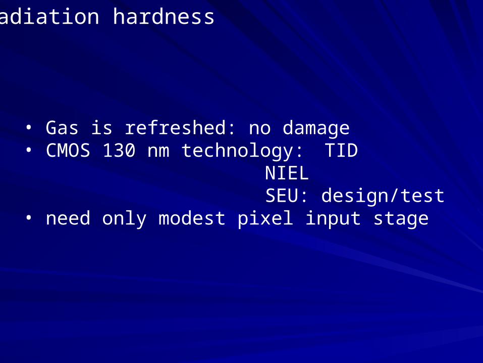
Radiation hardness
• Gas is refreshed: no damage• CMOS 130 nm technology: TID
NIELSEU: design/test
• need only modest pixel input stage
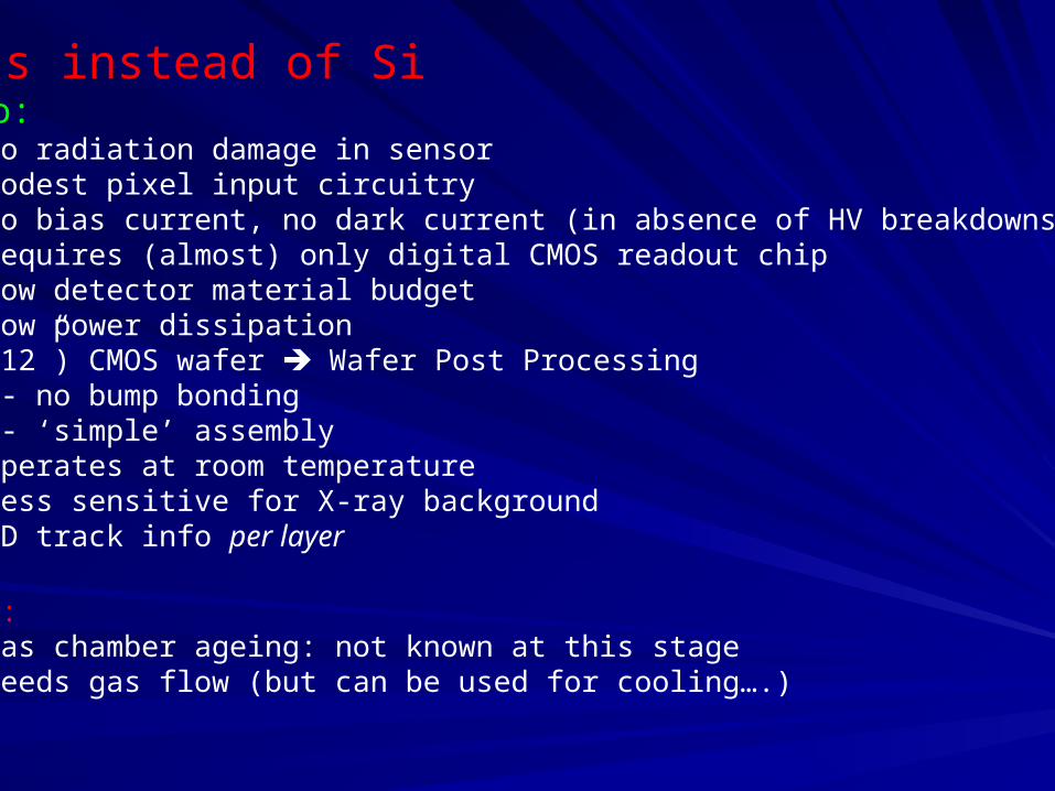
Gas instead of SiPro:- no radiation damage in sensor- modest pixel input circuitry- no bias current, no dark current (in absence of HV breakdowns..!)- requires (almost) only digital CMOS readout chip- low detector material budget- low power dissipation- (12”) CMOS wafer Wafer Post Processing
- no bump bonding- ‘simple’ assembly
- operates at room temperature- less sensitive for X-ray background- 3D track info per layer
Con:- Gas chamber ageing: not known at this stage- Needs gas flow (but can be used for cooling….)
Plans
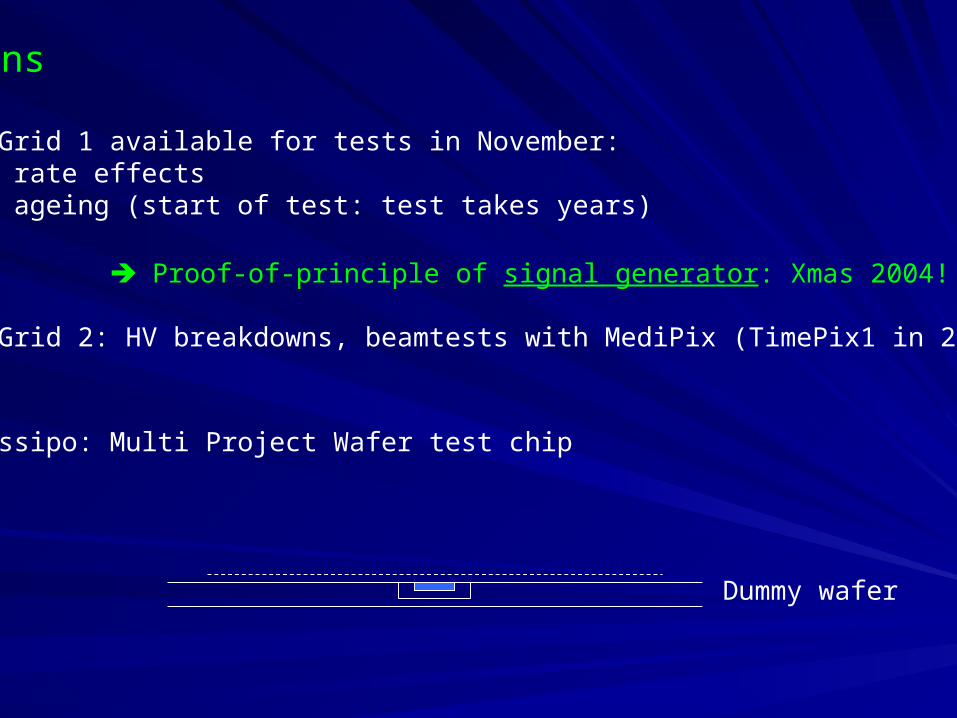
- InGrid 1 available for tests in November:- rate effects- ageing (start of test: test takes years)
Proof-of-principle of signal generator: Xmas 2004!
- InGrid 2: HV breakdowns, beamtests with MediPix (TimePix1 in 2005)
- Gossipo: Multi Project Wafer test chip
Dummy wafer
New gaseous detectors:the application of pixel sensors as direct anode
NIKHEF Auke-Pieter ColijnAlessandro FornainiHarry van der GraafPeter KluitJan TimmermansJan VisschersMaximilien
Chefdeville
Saclay CEA DAPNIA Paul ColasYannis GiomatarisArnaud Giganon
Univ. Twente/Mesa+ Jurriaan Schmitz
CERN/Medipix Constm Eric HeijneXavie LlopartMichael CampbellThanks to: