UNCLASSIFIED AD NUMBER AD916687 NEW LIMITATION CHANGE TO Approved for public release, distribution unlimited FROM Distribution authorized to U.S. Gov't. agencies only; test and evaluation; Dec 1973. Other requests shall be referred to RADC [DCCL], GAFB, NY 13441. AUTHORITY USAF, ltr, 12 Apr 1978. THIS PAGE IS UNCLASSIFIED
Transcript
UNCLASSIFIED
AD NUMBER
AD916687
NEW LIMITATION CHANGE
TOApproved for public release, distributionunlimited
FROMDistribution authorized to U.S. Gov't.agencies only; test and evaluation; Dec1973. Other requests shall be referred toRADC [DCCL], GAFB, NY 13441.
Distribution limited to U. s. Gov't agencies on~ly;test and evaluation, December 1973. other requestsf or this document must be refprred to RADC (DCCL),GAFB, NY 13441.
Laboratory Directors' FundProject 01710108
Rome Air Development CenterAir Force Systems Comrncnd
Griffiss Air Force Base, New York
WIDEBAND COHERENT COMMUNICATION AT VLF WITHTHE EXPERIMENTAL TRANSMITTING ANTENNA MODULATOR (ETAM)
John '. Gamble
Distribution limited to U. S. Gov't agencies only;"test and evaluation; December 1973. Other requestsfor this document must be referred to RADC (DCCL),GAFB, NY 13441.
Do not return this copy. Retain or destroy.
FOREWORD
This report effectively complements RADC.TR-72-212 entitled "Experimental Transmitting Antenna Modulator"which describes the design and in-plant testing of the antenna modulator as performed by Westinghouse ElectricCorporation under contract F30602-72-C-005 I. The effort described in this report is the in-house on-air perfomanccevaluation of the contractor produced equipment. Thus, these in-house results add to the contractor efforts describedin RADC-TR-72-212, to provide a complete coverage of the VLF/LF Transmitting Antenna broadbanding project
sponsored under Laboratory Directors' Funding, 01710108.
The author is indebted to Mr. G. A. Pfeiffer, Captain W. A. Acree, and Sgt. R. Klumpp of RADC for theirindispensable assistance in making the on-air measurements.
APPROVED: v A
GEORGE E. BRUNETTEChief, Communications Transmission BranchCommunications and Navigation Division
APPROVED: .'
FRED I. DIAMOND, Technical DirectorCommunications and Navigation Division
FOR THE COMMANDER:
CARLO P. CROCETTIChief, Plans Office
' ii
ABSTRACT
A 1-kilowatt Experimental Transmitting Antenna Modulator (ETAM) was tested on-air at RADC. This on-airperformance evaluation at 29.5 kHz employed a VLF transmitting station at Camden, New York and a receivingstation at RADC, Griffiss AFB, New York. Using the ETAM, an 800 baud coherent FSK (Modulation Index of1/2) signal was efficiently transmitted ever the 160 Hz 3 db static bandwidth transmitter/antenna system, con-currently, the signal was received and coherently demodulated with negligible evidence of intersymbol distortionor other system degradation. On the other hand, when the ETAM was removed from the transmission system, itwas necessary to derate the transmitter output power by 10 db to preclude destruction of the transmitter outputtransfoimer caused by the high-Q mismatched output load; under this operating condition, It was impossible toobtain bit error rates less than 6% because of the ambient atmospheric noise and intersymbol distortion. Thisreport describes the equipment configurations at the transmitter and receiver, the test procedures, and thequantitative results.
,'U
TABLE OF CONTENTS
Page
Section I Introduction ......... .................................................A. Report ..... .................................................. ...B. Significance of the Effort 1.........................................C. Background ........................................................D. Significance of the Report ......................................... 3
Section 11 Equipment and Subsystem Description .... .................................. 4A. The Experimental Transmitting Antenna Modulator (ETAM) ................... 4
1. Principle of Operation ............................................. 42. Description of Equipment .... .................................... 9
a. Tuner Coil ................................................... 9b. RF Switching Assembly ....................................... 9
(1) Turn On .... .......................................... !0(2) Turn Off .... ........................................... 10(3) Dynamic Damping .... .................................... 10
c. Control Cabinet .... .......................................... 10d. Zero Crossing Detector ... ..................................... 10
Section III Test Operation and Instrumentation .... .................................... 15A. Back-to-Back Configuration ... ....................................... 15B. On-Air Test Configuration ... ......................................... 15
Section IV Qualitative Results .... ................................................ 17A. Antenna Current Transient Response .... ................................ 17B. Received Signal .... .............................................. 20C. Effects of Installation on ETAM Operation and Reliability ...................... 21
1. False Switching Produced by RFI .................................... 212. Current Division in Parallel Parasitic Elements ......................... 223. Identification of Inoperative Switches ............................. 22
Section V Quantitative Results ............................................... 23Bibliography ......................... .................................... 25Appendix A Compatible Shift Keying (CSK) Modem .................................... 26Appendix B Reactance Modulation of VLF Antennas ............................... 33
"v
LIST OF ILLUSTRATIONS
Page
Figure 1. Passive Equivalent of Electrically Short Monopole ......................... 4Figure 2. Passive Equivalent Circuit for a VLF/LF Antenna System ........................ 5Figure 3. Antenna Modulator Design Principle ................................... 6Figure 4. ETAM Coupling .................................................. 7Figure 5. RF Switch Schematic ..... ........................................... .9Figure 6. ETAM Equipment ... ................................................ I IFigure 7. Transmitting System .... ............................................ 12Figure 8. Receiving System .... .............................................. 13Figure 9. Receiver Frequency Response .......................................... 14Figure 10. Back-to-Back Configuration .... ........................................ 15Figure i1. On-Air Configuration .... ............................................. 16Figure 12. Antenna Current Envelope with ETAM - "Idle" Data .......................... 18Figure 13. Antenna Current Envelope with ETAM - Random Data ........................ 18Figure 14, Antenna Current Envelope without ETAM - "Idle" Data ........................ 19Figure 15. Antenna Current Envelope without ETAM - Random Data ................... 19Figure 16. Received Signal Envelope with ETAM - "Idle" Data.. ........................ 20Figure 17. Received Signal Envelope without ETAM - "Idle" Data ....................... .21
Figure 18. Compatible Shift Keying (CSK) Modem Performance ... ....................... 24Figure A]. Output Bit Error Rate vs. Decision Error Rate (Differential Decoding) .. ........... 28Figure A2. Decision Error Rate for MSK Detection .................................... 31Figure A3. Output Bit Error Rate for CSK Demodulation ... ........................... 32Figure B1. Passive Equivalent of Electrically Small Antenna .............................. 33Figure B2. Passive Equivalent Circuit for a VLF/LF Antenna System ........................ 34
LIST OF TABLES
Table I. High Powered VLF/LF Stations .....................................Table II. ETAM Equipment Rating Summary ...................................... 10
vi
SECTION IINTRODUCTION
The objective of this effort was to evaluate the on-air performance of an Experimental Transmitting AntennaModulator (ETAM) developed by Westinghouse Electric Corporation. This antenna modulator rapidly tunes anarrowband VLF/LF antenna system in synchronism with the transmitted FSK signals. The antenna modulationis performed with minimum insertion loss and is suitable for operation at any frequency in the 20-00 ki lz range.It is designed to accommodate FSK signalling rates up to 1500 bits/sec and input powers up to one kilowatt.
A. The Report
Although the antenna modulator was successfully tested in-plant in conjunction with a high-Q simulatedazntenna load (a single-tuned series resonant circuit), this was not sufficient to assure its technical adequacy wherinteroperated with a real antenna system. Thus, this report describes the on-air testing of the antenna modularor.Specifically, it includes: (1) A description of the transmitting and receiving equipment; (2) A description of ti,.instrumentation; (3) A qualitative assessment of the effect of the ETAM on the communication link, includingphotographs of the antenna current envelopes to illustrate system response; and (4) quantitative results consistingof the measured bit error rate p-rformance of a coherent FSK modem with and without the ETAM in the system.
B. SignYicance of the Effort
This on-air test provides a real-world operational verification of the theoretical and laboratory feasibility ofefficiently transmitting wi'-eband FSK signals over an antenna system whose static bandwidth is much less thanthe signal bandwidth. The net effect of this technique is to greatly increase the effective bandwidth-efficiencyproduct of VLF/LF transmitting antennas for FSK signalling; this effect, not realizable by linear, time-invariantcircuit techniques, is achieved by utilizing time-variant antehna tuning inductance.
C. Background
Mathematical analysis has shown (see Appendix B) that modulation of high-Q tuned circuit reactance, if doneto coincide with the appropriate carrier phase, can shift the instantaneous resonance of the circuit at any ratewhich is an integral subharmonic of twice the resonant frequency; in other words, such a reactance shift can bemade after any arbitrary number of half-cycles of the resonant frequency. For a total shift, Af, of the resonantfrequency, f, if the driving voltage is of constant amplitude and shifted in frequency synchronously with thecircuit tuning, then the envelope of the circuit current waveform has a transient whose maximum amplitude isgiven by Af/f relative to the steady state amplitude. In a practical FSK transmitting system where the totalfrequency shift is a small fraction of the nominal carrier (center) frequency, the resultant antenna current isnearly constant; in turn, the radiated signal (proportional to the antenna current) will have a similar approximatelyconstant amplitude which is entirely suitable for coherent FSK demodulation.
Earlier practical efforts at implementing this technique, however, have been applied only to FSK at a signallingrate about the same as the antenna system 3 dB static bandwidth. This is shown in Table I where the characteristicsof some operational high-powered VLF/LF stations are listed; these stations currently use antenna modulation for50 baud (bits/sec) FSK signalling.
i~~~~rP I W, •3mK~lg~
TABLE IHIGH POWERED VLF/LF STATIONS (Reference 6)
Operator Location Power .3 dB Static Bandwidth
US Air Force Hawes, California 100 KW 65 liz @ 27 kHzUS Air Force Silver Creek, Nebraska 100 KW 65 Hz @ 27 kHzUS Navy Cutler, Maine 2 MW 70 Hz @ 18 kHzUS Navy Annapolis, Maryland 200 KW 33 Hz @ 20 kHz
Thus, although theory predicts the feasibility of signalling rates much greater than antenna static bandwidths,current operational practice has employed antenna modulation for FSK signalling rates comparable to antennastatic bandwidths; in these cases, the antenna modulation serves to minimize the instantaneous load phase angleat the transmitter amplifier outputs and hence, to maximize amplifier efficiencies.
On the other hand, the ETAM was specifically developed to investigate and implement the antenna modulationtechnique for wideband FSK signalling with statically narrowband VLF/LF antenna systems. (A completedescription oh the design and principle of operation is contained in RADC TR-72-212 (Reference 3), but forcompleteness in this report, a brief description is presented in Section II). The ETAM was tested in-plant, utilizinga single-iuned series resonant circuit to simulate a high-Q (100 Hz static bandwidth at 37 kHz) low frequencyantenna circuit. This simulated antenna system was driven by a I KW solid state amplifier which in turn wasexcited by an FSK modulator; the ETAM was used to resonate the antenna circuit in synchronism with the FSKmodulation. The system was operated at modulation reversal (alternating upward and downward frequency shifts)rates of 200, 1000, and 1600 bauds; the corresponding frequency shifts were 100, 500, and 800 Hz, respectively,and the input power was 1000 watts for the lower rates and 300 watts for the highest rate. The principal apparentdistortion in the output (antenna current) was, as theoretically predicted, amplitude steps of less than 5% at theinstants of frequency shift. The apparent insertion loss was less than .3 dB. Finally, a measurement of intersymboldistortion, D, was made according to
D= 1 - f°TT (f, t) SR (f, t) dt
fý [SR (f, t)] dt
where:(A cos 27rf t 0<tKT
A cos 27rf 2 t t<O
Undistorted input signal to theantenna system
SR (f, t) = B cos (27rft + 0)= Steady state antenna output
Signal produced by the constantinput signal A cos (27rf, t).
ST (f, t) = Output signal produced by theinput signal S, (f, t) where
1f2- fl1 I= 1 (I)2T
2
W P.'-
Thit measurement yielded D < .05 for FSK signalling et 1000 bauds. The clear implication of these in-plant testresults was that the ETAM should permit high efficiency (nearly equivalent to constant amplitude, constantfrequency signal radiation) FSK transmission up to 1600 bauds over any antenna system whose static handwidthwas at least 100 Hz. Nevertheless, these satisfactory in-plant test results did not guarantee similar successful on-airperformance. The effort described heroin was thus undertaken to measure the real-world, on-air performance of theETAM with random FSK modulation.
D. Significance
This report presents the practical validation ot the ETAM design principle.
The earlier theoretical analyses, baied on the principle of resonant transfer of stored electrical energy in reactive11v networks and the application of Laplace transforms to the time-variant system response clearly implied the physical
validity of the ETAM.approach. The contractor development and in-plant test with the simulated antenna networkreduced the theoretical approach suggested in the literature to practice, wherein the reactance modulation rate wasfar greater than the static bandwidth of the passive simulation network. This present effort, then. finally appliedthe reactance modulation technique to a practical anteuna system; moreover, this practical implementation of theETAM involved significant Input power - much more than had been utilized in small-signal (10 watts or less)reactance amplifier approaches such as proposed by Vallese (Reference 5).
i -1r
l 3
SECTION IIEQUIPMENT AND SUB-SYSTEM DESCRIPTION
The on-air test of the ETAM was conducted at the RADC Camden, New York, test annex and at RADC, GriffissAFB, New York. The ETAM was operated in conjunction with the experimental low frequency transmitting stationat Camden, and the transmitted signals were received at RADC. The following sections describe (A) the operationalprinciple and design of the ETAM; (B) the equipment configuration at the transmitting siation; and (C) the equip-ment configuration at the receiving station.
A. The Experimental Transmitting Antenna Modulator (ETAM)
1. Principle of Operation
In Figure 1, a passive network is shown which closely approximates the electrical characteristics of anelectrically short monopole (or top-loaded monopole) antenna. The term "electrically short" is appropriate whenthe operating frequency is much lebs than the natural dipole resonance frequency of the antenna system, or, inother words, the length of the antenna is much less than 1/4 the free-space wavelength of the signal to be trans-mitted. Under this condition, the antenna structure is effectively a series capaoitance and resistance. Because ofthe electrical shortness of the antenna, both the capacitance, Ca' and the rai'iation resistance, Rr, are necessarilysmall. The loss resistance, RL, produced by ohmic losses in the antenna and ground system is customarily mini-mized in design and construction so as to maximize efficiency; the antenna efficiency is given by
Rr
7 = Rr +R(2)77=Rr + R-"--
RL
C a
Rr
Figure 1. Passive Equivalent of Electrically Short Monopole
However, the low value of capacitance of the antenna structure causes such a short monopole to be a highlyreactive electrical load for a power transmitter. This is compensated for by the inclusion of a series inductor orhelix of proper inductance to produce series resonance, and hence a resistive transmitter load, at the desiredfrequency. This typical low frequency equivalent antenna circuit is shown in Figure 2.
4
~VV"
Ca
POWER TRANSMITTER
Figure 2. Passive Equivalent Circuit of a VLF/LF Antenna System
Just as the inherent antenna and ground losses must be minimized for system efficiency, so must the ohmic
losses in the tuning inductance; in Figure 2, the resistance of the coil is combined with the other antenna system
loss reAstances in the term RL. Here, the series resonant circuit is a very high-Q network where Q is defined by
QA 2rfL _2 (3)- Rr + RL + Rg 21rfCa(Rr + RL + Rg)
where Rg is the source resistance of the transmitter amplifier represented in its Thevenin equivalent form, and Fis the operating frequency.
The static half-power (3 dB) bandwidth of tlds network is given by
B 3 Rr+RL+RG - f21rL Q
where f = is the operating frequency.
Customarily, such a fixed-tuned antenna system used for FSK transmission would be tuned to a frequencyintermediate between the upper and lower FSK shift frequencies. This balances the degradation of the outputsignal amplitudes at the two shift frequencies, but it also results in the antenna system being slightly detunedfrom resonance at all times during FSK transmission. This prompted the development of antenna modulationto alleviate this situation. (As discussed in Section I, operational applications of this technique permit maximumFSK signalling rates comparable to the antenna static bandwidths).The following discussion describes the antennamodulation technique.
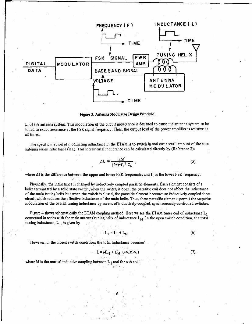
Consider the functional representation of Figure 3. The input to the system is a binary voltage waveform(digital data) which drives a frequency shift keying (FSK) modulator. The modulator produces two outputs: (1)a constant envelope radio-frequency sinusoid whose frequency is shifted in accordance with the input digital dataand (2) a rectangular baseband waveform whose voltage is stepped up and down in synchronism with the frequencyshifts of the FSK signal output. The FSK signal is then amplified and applied directly to the antenna system. Onthe other hand, the baseband output drives the antenna modulator whose function is to vary the effective inductance.
5
FREQUENCY ( F) INDUCTANCE ( L)
T I" - --E T I M E
TI MEDIGITAL MODULATOR 1AMP.IDATA BASEBAND SIGNAL JU
]VOLTAGE T ANT E NNA(
&i MO DU LATOR
STIME
Figure 3. Antenna Modulator Design Principle
L, of the antenna system. This modulation of the circuit inductance is designed to cause the antenna system to betuned to exact resonance at the FSK signal frequency. Thus, the output load of the power amplifier is resistive atall times.
The specific method of modulating inductance in the ETAM is to switch in and out a small amount of the totalantenna series inductance (AL). This incremental inductance can be calculated directly by (Reference 3):
AL 2Af (5)AL . (2,r) 2 f1
3 Ca
where Af is the difference between the upper and lower FSK frequencies and f, is the lower FSK frequency.
Physically, the inductance is changed by inductively coupled parasitic elements. Each element consists of ahelix terminated by a solid state switch; when the switch is open, the parasitic coil does not affect the inductanceof the main tuning helix but when the switch is closed, the parasitic element becomes an inductively coupled shortcircuit which reduces the effective inductance of the main helix. Thus, these parasitic elements permit the stepwisemodulation of the overall tuning inductance by means of inductively-coupled, synchronously-controlled switches.
Figure 4 shows schematically the ETAM coupling method. Here we see the ETAM-tuner coil of inductance L1connected in series with the main antenna tuning helix of inductance LM. In the open switch condition, the totaltuning inductance, LT, is given by
LT =L + LM (6)
However, in the closed switch condition, the total ir~ductance becomes
L=ML + 0M, O<M 1 (7)
where M is the mutual inductive coupling between L1 and the sub coil.
.6
Hence, we have
AL =LT - L= (I - M)L! (8)
ANT.LITUNERCOIL MAINLMTN GHLI
TRANSMffTERe _.O__ -
OUTPUT
SU1B COISOLID STATE
rIWITCH (EQUIVALENT)I
Figure 4. ETAM Coupling
Before proceeding to a more specific description of the ETAM equipment, it is appropriate to consider twoimportant constraints in the operation of ETAM with a high-powered transmitting system. The first overallsystem constraint is that of signal waveform continuity. Because the antenna system is a high-Q load for the trans-mitter, it is mandatory that the RF waveform be continuous at all times, including frequency shift transitions.If this constraint is not observed, drastic antenna current amplitude and phase transients result which precludeefficient system operation and may be destructive to transmitter amplifiers operating at or near full power. The.second constraint, specifically related to the ETAM operation, is that shifts of inductance must occur when theinstantaneous current in the antenna circuit is nearly zero. The reason for this constraint is a corollary of thehigh-Q of the antenna circuit; because Q can also be defined as the ratio of the maximum energy stored in thereactive components, 1/2 LI 2 or I/2CV2 , to the average energy dissipated per radian of the signal waveformRj 2 /47f, where I is the current amplitude and f is the waveform frequency, substantial energy is stored in themagnetic field of the inductance on a time-periodic basis. This instantaneous stored energy in the magnetic fieldof the inductor is proportional to the square of the instantaneous antenna current; thus, the proper time forswitching the inductance value is at a current zero. Conversely, a change of inductance, when the current is nearits semi-periodic maximum magnitude, will result in voltage transients potentially destructive to switching com-ponents and excessive transients in the current envelope.
However, if inductance switches are constrained to occur at current zeros (this is an idealization, since anypractical switch requires a finite time to change from "on" to "off" or vice-versa), then the expected maximumtransient on the current envelope can be determined by stored energy considerations. If the current in the antennacircuit of Figure 2 is at steady state at the upper frequency, f2 , the toial stored energy in the circuit is given by
U2 1/2 L 122.= 1/2 CaV22 (9)
where V2 12 (Rr + RL + RG) and
f2 1 (10)
2n r LCE'a
As previously stated, the total stored energy is in the magnetic field of the inductor when the current is maximumand the voltage zero; in the case where the current is zero and the voltage at the antenna base is maximum, the totalstored energy is in the electrostatic field of the antenna structure-grounding system. Considering the case where thecurrent is maximum (12), we have from (9) and (10):
2U rf 2 C22LCa (11)
Now, if the inductance is instantaneously increased from L to L + AL at the next current zero crossing, thecircuit immediately becomes resonant at frequency F1 given by
1l= (1 2)
21r V (L + AL) Ca
However, the circuit energy cannot change appreciably during the next quarter RF cycle (because of high circuitQ) so that the peak current at the end of the quarter cycle is given by
12' L+AL 2= f 21f, /2U 2 Ca (13)
Thus, the ratio of the current after a downward frequency shift to the current just before the shift is given by
-2 fl f2-(f2-fl) f- (14)
12 f2 f2 f2
Now, assuming f2 - f, <<f 2 , then f, - f2- (f, + f2 ) A f (15)
(where f is the nominal unmodulated carrier frequency), and
12 , 1 12 - f l (16)12 f
Now, considering the alternate situation where the current is at steady state at the lower frequency f1 , weobtain U, = 1/2(L + AL) 112 = 1/2 CaV12 so that I
V + L - 2fff I2U• Ca (17)
Again postulating a change of inductance at a current zero, but this time a decrease by AL, we obtain themaximum current a quarter cycle later
I1l =27rf2 2U,' Ca (18)
Here, the ratio of the current a• an upward frequency shift to the current just before the shiff is given by1' f1 f2 -1 - 2 )f19
! f I fl 2 + (flI - f2) . + f2---- (19)
I1 f2 f2 f
Since f2 - fl<<f, the latter term of both (16) and (19) will be a small fraction of the steady state currentamplitude, but this is the maximum transient effect to be expected on the antenna current envelope. It should
8
be noted that this transient term in the current amplitude expression is only applicable at a frequency shift point:with increasing time, the transient component decays to zero in accordance with the circuit Q so that the overallcurrent tends to its steady state amplitude. Thus, the effect of circuit Q is to limit the recovery rate of the currentenvelope to steady state after a frequency shift; however, it is obvious that the maximum current amplitudetransient represents a very small fraction of the overall current amplitude. Hence, the output current envelope isnearly constant and for the analysis of phase coherent modem systems, a constant envelope approximation is valid.
2. Description of Equipment
A 1-kilowatt model of the ETAM tuner was built for both laboratory and field test evaluation. This equip-ment consisted of the followirg major assemblies:
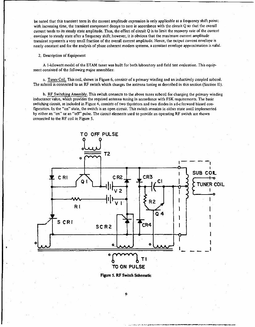
a. Tuner Coil. This coil, shown in Figure 6, consistr of a primary winding and an inductively coupled subcoil.The subcoil is connected to an RF switch which changes the antenna tuning as described in this section (Section 11).
b. RF Switching Assembly. This switch connects to the above tuner subcoil for changing the primary windinginductance value, which provides the required antenna tuning in accordance with FSK requirements. The basicswitching circuit, as included in Figure 4, consists of two thyristors and two diodes in ad-c forward biased con-figuration. In the "on" state, the switch is an open circuit. This switch remains in either state until implementedby either an "on" or an "off" pulse. The circuit elements used to provide an operating RF switch are shownconnected to the RF coil in Figure 5.
TO OFF PULSE
""2
I- - I
CCRCR2 CR3 I SUB COL
RR2 !RIR
04 I IR I
CR K I
ogY'v~ TITO ON PULSE
Figure S. RF Switch Schematic
C
This circuit performs the following three basic functions:
(1) Turn-On. Turn-on is initiated by applying a single positive pulse to the gates of SCRI and SCR2simultaneously. This causes these SCR's to start conducting in the forward direction, resulting in a d-c latchingcurrent provided by the source VI around the loop Ri, SCRI and SCR2. Steering diodes CR1 and CR2 are usedto restrict this latching current to the SCR loop only. This latching current (approximately 3 amperes) is sufficientto maintain continuous conduction in the SCR's. The circuit now performs as a closed bi-directional switch to theRF current supplied by the subcoil, with one polarity of the RF cycle flowing through CR1 and SCRi, and theopposite polarity flowing through CR2 and SCR2. This switch will remain in this closed state until the latchingcurrent is interrupted sufficiently long to permit each half of the RF cycle to pass through zero.
(2) Turn-Off. To return the RF switc.. to the "off' state, a positive pulse is applied to the base of Q1,which conducts and hence removes the latching current to SCRI and SCR2. The turn-off time is reduced byreturning the base of Q I to a negative voltage (V2) which provided some forced turn-off commutation for SCRIand SCR2. The switch is now open and will remain in this state until an "on" pulse is applied.
(3) Dynamic Damping. This part of the circuit is used to suppress voltage overshoot when the switchtransfers from the "on" state to the "off" state. Although a transition occurs when the switch current is zero, astep function in voltage occurs when the switch stops conducting. This is due to the 900 phase relationshipbetween the voltage and the current. The step function, unless suppressed, will subject the SCR's to voltagetransients in excess of their rating, which can result in device destruction. This transient is suppressed by chargingCl, using a full-wave rectifier circuit consisting of CR3 and CR4, and occurs during the RF switch transition fromthe "on" to the "off" state. As the transistor Q4 is off during the entire RF switch "off" state, capacitor C l willcharge to the peak open circuit voltage of the subcoil. This charge is removed during the RF switch "on" state byapplying a positive pulse to the base of Q2 of sufficient duration (approximately 100 usec) thus reducing thiscapacitor voltage to zero as required for transient suppression during the next RF switch transition from "on"state to the "off" state.
The RF switch assembly, as shown in Figure 6, is air cooled by a self-contained fan.
c. Control Cabinet. This cabinet, also shown in Figure 6, contains all of the controls, power supplies, logic.and pulse drivers as required to operate the RF switches.
d. Zero Crossing Detector. This unit consists of a current transformer, which samples the antenna current,and a full-wave detector connected to the secondary of this current transformer. The output, therefore, supplieszero pulses every 1800 of the operating frequency and is used as one of the inputs to both the "on" and the "off"logic.
A summary of the pertinent ETAM characteristics is presented in Table II below:
TABLE IIETAM EQUIPMENT RATING SUMMARY
AC power source 60 Hz 120 V 5 AAntenna curretnt 6A RMS min. - 26 A RMS max.Tuning coil RF voltage to ground 500 V RMS max.Tuning coil PRI inductance (switch open) 92 MHTuning coil PRI inductance 91.6 pH max.
(switch closed) 37.5 pH min.Data input impedance 100 ohmsData input voltage (Positive) min. 4 V max. 6 V
10
TABLE 11ETAM EQUIPMENT RATING SUMMARY (Continued)
Data input pulse width (usec) 2 min., 10 max.RIF switch current 20 A (peak) max.RF switch voltage 600 V (peak) max.RF frequency range 20 kHz to 60 kHzSquare wave input voltage (test) 4 min., 10 max.Square wave input impedante (test) 2 kohms
CONTROL CABINET j J In
'ZERO7CRSSING D ETECTOR
Figure 6. -ETAM Equipment
B. The Transmitting Station
The ETAM was installed at the Camden, New York experimental VLF/LF transmitting station. Figure 7 is ablock diagram of the overall transmitting system.
ETAME T A M 5' ANT
-CURRENT AZERO -CROSSING. IJ
I DETECTOR, PRIMARY HEMAIN
DAA 9. HZFS 4ETAM 1 CI
[IMH~ i I SWITCH'8
CLOCK I CONTROL 1
Figure 7. Transmitting System
The following is a brief description of the signals and equipment represented on the diagram (except for the ETAMcomponents previously described):
I. Data. The data which was used to drive the modulator consisted of baud synchronous (all elements ofequal length) digital data at a rate of 800 bauds (elements/second). The data was formatted into frames of 15elements each where the fifteenth element was a binary I synchronization pulse.
2. Modulator. The special modulator generated two outputs, the FSK signal for RF transmission and abaseband rectangular voltage waveform synchronous with the FSK modulation (see Figure 3). The 800 baud FSKsignal was derived by precise digital frequency division from a stable 1 MHz clock (or oscillator); this techniquegives the spectral components of the FSK signal a coherent time base such that coherent demodulation by asuitable receiver is possible. The modulation index of the FSK waveform was .5 which means that the differencebetween the upper and lower FSK frequencies in Hz is equal to one half the baud rate. (In this system, the totaldifference between FSK frequencies was exactly 400 Hz.) Here, the upper shift frequency corresponds to a binary"0" and the lower shift frequency to a "1".
3. Clock.The 1 MHz Clock (or oscillator) was a Hewlett-Packard 5 1OA.
4. Transmitter. The AN/FRT-19 Low Frequency Transmitt.: is a linear Class B 15 KW tube-type amplifier.It is designed to operate in the nominal range of 30 kHz to 300 kHz.
5. Main Helix. The main tuning helix consisted of air-core Litz-wire coils for coarse tuning and a ferrite-loaded varicoupler for fine tuning. The mean inductance of this component of the system was 4100 ph.
12
6. Antenna. The low frequepcy antenna is a 625 foot top-loaded monopole with the following characteristics
at 29.5 kHz:
0 Static Capacitance - 7000ppuf* Radiation Resistance - .114920 3 dB Static Bandwidth - 160 Hz* Radiation System Efficiency (CW signal) - 5%* Maximum Base Voltage - 30 KV
C. The Receiving Station
The FSK signal was received and demodulated by a receiver subsystem located at Griffiss AFB, New York,some 26 miles from the transmitting station at Ca, uden. Figure 8 is a block diagram of the receiver subsystem.
I R-1408 101KIHe IF CSK DEMODULATORRECEIVER 8 0 B U
LOOPANTENNAAS 1917 FRI I IMHE I
I M D-6 90
DEMODULATOR
f TD-818 3 MHZ Clock0 S CI LLATOR
I AN/ARC96 IRECEIVER
I _ S U BSYSTEM _
Figure 8. Receiving System
The various components of this receiving system are discussed below:
1. Loop Antenna. The receiving antenna was a crossed loop system, model AS1917FR, which is usedoperationally in the 487L Survivabit Low Frequency Communication System ground receiving stations.
2. Receiver. TheR-1408/ARC-96 Receiver is a VLF/LF receiver designed for operation in the 14-60 kHzrange. It was operated in conjunction with the depicted MD-690/ARC-96 and TD-818/ARC-96 components whichconstitute an integral part of the AN/ARC-96 (airborne portion of the 487L system) receiver subsystem; however,for this test, the only function of the TD-818/ARC-96 and MD-690/ARC-96 was to provide the essential 1 MHzclock signal to the R-1408 receiver and the 3 MHz clock signal to the special 800 baud CSK demodulator as shownin Figure 8. The essential output of the R-1408 receiver was a hard-limited 10 kHz IF signal. Figure 9 shows a plotof the normalized frequency response of the R-1408 receiver, H(f) H(f)*/H(0)H(0)* -- where H(f) is the receivercomplex transfer function, in a linear mode of operation (the hard limiter was inoperative for this measurement):from this data, the effective noise bandwidth of the receiver was calculated to be 469 Hz, substantially less thanthe FSK transmission rate.
13
0. 7
i 0.6
*
"I-x
TO .S
0.2
0.2 //
-62S. -37S. --12S. 12S. 37S. 62S.
FREQUENCY OFFSET. F. iN HZ
Figire 9. Receiver Frequency Response3. CSK Demodulator. The 800 baud Compatible Shift Keying (CSK) demodulator coherently demodulatedthe 800 baud FSK signalling from the hard-limited 10 kHz IF signal. The CSK demodulation process is described inAppendix A, and its detection efficiency in Gaussian noise is shown to be virtually equivalent to the theoretically-
optimum coherent biphase or quadriphase shift keying (PSK) detection.
14
SECTION IIITEST OPERATION AND INSTRUMENTATION
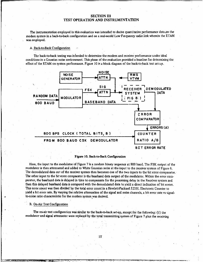
The instrumentation employed in this evaluation was intended to derive quantitative performance data on themodem system in a back-to-back configuration and on a real-world Low Frequency radio link wherein the ETAMwas employed.
A. Back-to-Back Configuration -
The back-to-back testing was intended to determine the modem and receiver performance under idealconditions in a Gaussian noise environment. This phase of the evaluation provided a baseline for determining theeffect of the ETAM on system performance. Figure 10 is a block diagram of the back-to-back test set-up.
NOISE NOS FRvs IGENERATOR AT --" VTVMI
FSK SI :GRECEIVER DEMODULATEDATTN L SYSTEM DATA
R ANDOM DATA MODULATORFI 8.
800 BAUD BASEBAND DATA - - -
E RROR 1CCONIPARATORj
ERRORS (A)
800 BPS CLOCK (TOTAL BITS, B) COUNTER 1FROM BOO BAUD CSK DEMODULATOR RATIO A/B
BIT ERROR RATE
Figure 10. Back-to-Back Configuration
Here, the input to the modulator of 'Figure 7 is a random binary sequence at 800 baud. The FSK output of themodulator is then attenuated and added to White Gaussian noise at the input to the receiver system of Figure 8.The demodulated data out of the receiver system then becomes one of the two inputs to the bit error comparator.The other input to the bit error comparator is the baseband data output of the modulator. Within the error com-parator, the baseband data is delayed in time to compensate for the processing delay in the Receiver system andthen this delayed baseband data is compared with the demodulated data to yield a direct indication of bit errors.This error count was then divided by the total error count in a Hewlett-Packard 5233L Electronic Counter toyield a bit error rate. By varying the relative attenuation of the signal and noise channels, a bit error rate vs signal-to-noise ratio characteristic for the modem system was derived.
B. On-Air Test Configuration
The on-air test configuration was similar to the back-to-back set-up, except for the following: (1) themodulator and signal attenuator were replacqd by the total transmitting system of Figure 7 plus the receiving
15
antenna of Figure 8, and (2) the baseband data link of Figure 10 included a wideband microwave link to carry thebinary reference data to the error comparator co-located with the receiver system. Figure I I is a block diagram ofthe on-air test configuration.
ASK (MICROWAVE) -O AM COMPmoo _ CHANNEL I RCVR ERRO R W)
FROM 800 BAUD CSK D EMOD A / B
BIT ERRORS
Figure 11. On-Air Configuration
In this latter configuration, the baseband data was used to produce an on-off-keyed (or Amplitude Shift Keyed,ASK) waveform at a carrier frequency of 40 kHz. This signal was then transmitted via a wideband (50 kHz band-width channel) microwave link from the Camden, New York, test facility to Griffiss AFB and the microwave-baseband output was detected at 40 kHz by a Honeywell 6869 VLF Receiver; because of the 40-50 dB signal-to-noise ratio at the Honeywell receiver output, this demodulated signal provided a virtually error-free binaryreference for comparison with the signal processed through the Low Frequency Transmitter/Receiver system(Figures 7 and 8). Apain, the counter yielded the bit error rate - but in this case, it was the bit error rate, on-air,and with the ETAM in operation.
16
SECTION IVQUALITATIVE RESULTS
Although this evaluation was primarily intended to determine the quantitative effect of the ETAM on VLF/LFsystem performance, some qualitative observations of the ETAM performance are of significant interest. Theseinclude the observed antenna current transient response with and without the ETAM operating, the received signalenivelope with and without the ETAMoperating, and the effects of installation on ETAM operation and reliability.
A. Antenna Current Transient Response
As developed in Section II, the expected maxi'uum current transient relative to steady state current, A[, isgiven by
Al = f(to+) - f(to)AI=-I .(20)
where f(t0+) is the frequency immediately following a frequency shift at time to from the frequency f(to-) justprior to to and I is the steady state current amplitude.
In the system under test, f= 29.5 kHz, and If(t+) - f(to) I= 400 Hz so that, the maximum relativetransient would be
-L- 1 400.0136 (21)1 29500
Figures 12 and 13 are oscilloscope photographs of the actual antenna current envelope with the ETAM inoperation. Figure 12 shows an "idle" baseband data sequence and the corresponding antenna current envelopewhere fourteen bits are spaces (upper FSK frequency) and each fifteenth bit is a mark (lower FSK frequency).Figure 13 shows the antenna current envelope for a random FSK sequence more typical of actual communicationsignals. In both cases, it can be seen that the actual transient in the antenna current is very minimal. Although thecurrent envelope photographs do not give sufficient resolution to accurately measure the transient effect andverify the theoretical prediction of a 1.36% step, they do qualitatively show that the maximum antenna currentamplitude transient will be very small.
On the other hand, the current response of a 160 Hz bandwidth network to an 800 baud FSK input signalwould reasonably be expected to be substantially distorted in comparison with the response of a resistive, orinfinite bandwidth network. Similarly, the VLF antenna system with a static bandwidth of 160 Hz and withoutthe aid of the ETAM, should also have a substantially distorted current response to the 800 ba'-d signal. This isclearly shown by the current envelope photographs of Figures 14 and 15. Figure 14 shows an "idle" data sequenceand the corresponding antenna current eni'elope. Figure 15 shows a'random baseband data sequence and corre-sponding antenna current envelope. The amplitude distortion on the current output produced by the narrowstatic bandwidth is clearly apparent.
Thus, the efficacy of the ETAM in maintaining a nearly constant maximal current in an otherwise band-limiting antenna system is graphically shorn.
17
Figure 12. Antenna Current Enve-ope without ETAM - "Idle" Data
Figure 13. Antenna Current Envelope with ETAM - Random Data
18
Figure~~~~~~~~~.... 14..en.uret.vlpewtotEAM-"d"Dt
Figure 14. Antenna Current Envelope without ETAM - Random" Data
19
B. Received Signal
In addition to antenna current envelopes, observations were made of the envelope of the signal as received inthe antenna "far-field" at Griffiss AFB, N.Y. Because of the low radiation efficiency of the Camden transmittersystem at 29.5 kHz, the maximum radiated power with the ETAM (observing the maximum antenna currentlimitation of 25 amperes from Table II) was only 71 watts. This resulted in a signal-to-atmospheric noise ratio onthe order of 15-20 dB at the Griffiss based receiver, and thus perturbations of the observed signal envelope wereas much due to received noise as to transient effects produced by the ETAM. Moreover, received signal transientswhich clearly corresponded to FSK frequency shifts are believed to be primarily the response of the Honeywell6869 receiver to FSK modulation rather than an indication of transmitted signal envelope distortion. Nevertheless,the oscilloscope photographs do indicate the relative significance of frequency shifts in producing envelope transientson the received signal.
Figure 16 is an integrated (multiple exposure to compensate for low signal/noise ratio) photograph of theenvelope of the 29.5 kHz signal in a 3 kHz receiver bandwidth (Honeywell 6869) where the FSK modulationcorresponded to the "idle" data pattern (i.e. 14 upper frequency space bits and one lower trequency mark bit);tlhe upper trace shows the corresponding demodulated signal. It can be seen that the maximum pertjrabation of thereceived current envelope (located approximately 4 msec earlier (left) on the lower trace which corresponds to thedifferential demodulation delay) is minimal for the frequency downshift and upshift 1.25 msec later. This clearlyaffirms the previous contention that the radiated signal, just as the transmitting antenna current, is nearly constantwhen the ETAM is employed in the system.
Figure 16. Received Signal Envelope with ETAM - "Idle" Data
On the other hand, operation of the system without the ETAM produced the integrated oscilloscopephotograph of Figure 17 for the "idle" pattern. The similarity of this received signal envelope to the antenna:urrent envelope of Figure 14 is readily apparent. In both instances, the unmodu!ated narrow band antennasystem produced a significant amount of pulse-stretching which is apparent in the case of the isolated "mark"binary data element. (It should be noted that the rectangularity of the demodulated data elements (upper traceof the oscilloscope presentation) in Figures 16-17 is a result of pulse reshaping in the CSK demodulator).
Based on the observed characteristics of the received signal, it is apparent that tile ETAM does permit thetransmission of high rate FSK at VLF/LF over high-Q antenna systems with a minimum of amplitude distortion.Although this implies that the overall transmitter system with the ETAM may bc nearly as effective as a truewideband (antenna static ba-ndwidth substantially greater than the FSK signalling rate) antenna system of the
20
Figure 17. Received Signal Envelope without ETAM - "Idle" Pattern
same "on-tune" radiation efficiency, these qualitative amplitude results cannot really verify the quantitative modemsystem performance, especially in conjunction with the hard-limiting operational R 1408 receiver. (However, thequantitative bit error rate results presented in Section V do show this implication to be true).
C. Effects of Installation on ETAM Operation and Reliability
In addition to the preceding observations which were pertinent to validating the functional principles of theETAM, there were other factors bearing on the design and installation of both the 1KW model ETAM and anyhigher powered version. These included: (1) problems of false switching caused by RFI from the adjacent highpowered transmitter; (2) difficulty in adjusting the two parallel parasitic coils for equilization of current divisionduring conduction (switches on); and (3) difficulty in rapid identification of the inoperative switch in case of asilicon controlled rectifier (SCR) failure. Since these problems could be effectively handled in a future design, itis appropriate here to provide a brief discussion and a most likely design correction.
1. False Switching Produced by RFI. During the course of the on-air evaluation (three weeks) some4 SCR'sfailed, although these devices were operated well below their maximum current-voltage ratings. Because falsetriggering of the switches caused by RFI pickup in the ETAM control circuitry was noted at times, it is believedthat this was the principal cause of SCR failure. The reason for this suspicion is that closing the SCR switches ata high instantaneous current point on an antenna current cycle would require the nearly instantaneous dissipationof substantial energy stored in the magnetic field of the tuning inductance. Mathematically, this energy would bespecified by
U= 1/2 ALl 2 (22)
where I is the instantaneous antenna circuit current and AL is the change of inductance produced by the ETAM.
In order to preclude RFI-induced false triggering, it is essential that all small-signal control circuitry becompletely RFI shielded to isolate it from an adjacent high power transmitter. Likewise. such shielding might benecessary in a higher-powered system to prevent positive feedback from the high power sections of the antennamodulator itself.
21
2. Current Division in Parallel Parasitic Elements. A difficulty noted in the adjustment of the FTAM was inachieving approximately equal inductive coupling of the two parasitic coils to the main tuning helix. An imbalancein coupling will produce a corresponding imbalance in current division between the parallel elements; obviously, thiscould cause component current-voltage ratings to be exceeded in inmb, idual switch sections even though the com-posite (parallel coil and switch) system rating is not exceeded. Although current imbalance is not believed to havebeen the primary cause of SCR failures in the on-air test, it may well have been a contributory factor. However,proper current division is believed to be the most significant technical risk area in a high-powered antenna modulatorsystem wherein multiple parallel switches must be used. FoL this reason, gang tuning and integrated feedback controlare believed to be essential in a high-powered implementation of the ETAM technology.
3. Identification of Inoperative Switches. In the ETAM on-air tests, the failure of a solid state switch neces-sitated a lengthy "trouble-shooting" procedure to identify the inoperative section. Since the ETAM employs onlytwo such switching sections, this already lengthy diagnostic procedure would be a smill fraction of that required fora high-powered system of tens to hundreds of similar switch sections. Thus, it was apparent that suitable functionalindicators would have been very useful for ETAM operation and maintenance; it is also clear that functional indi-cators and protective circuitry, to prevent current overloads resulting from component failures, is mandatory in ahigh-powered antenna modulator system.
2
22
SECTION VQUANTITATIVE RESULTS
The preceding in-plant tests of the ETAM and the qualitative performance results of Section IV all insplrqdconfidence that the ETAM could greatly enhance the efficient transmission and reception of wideband FSK signals.
{• However, with the exception of the In-plant "intersymbol distortion test" described In Section 1, all of the in-plant
and qualitative results thus far only verified that wideband FSK could be transmitted and not necessarily receivedand demodulated at high efficiency. This determination of detection efficiency was the principal question left•i unanswered by the in-plant tests on a simulated antenna system, and was, of course, the principal motivation
behind the presently described on-air e'aluation. Moreover, this evaluation employed coherently detectable FSKsignals derived from random binary data, rather than the deterministic, but non coherent, modulation reversalsignals of the in-plant test; thus, the on-air tests were fully representative of state-of-the-art VLF/LF communicationtechnology because of the use of realistic signalling sequences, coherent modems, and the advanced R-1408
¶•: operational receiver. The specific results presented here consist of measured bit error rates as a function of signal.to-noise ratio where the noise is additive white Gaussian noise. By employing the instrumentation and operational
procedures described in Section lII,bit error rates were measured for the 800-bit coherent FSK system both back-S~to-back and on-air.
Figure 18 is a plot of bit error rates versus signal-to-noise ratio referenced to the detection bandwidth, or 800 Hz.The measured performance, both back-to-back and on-air with the ETAM, is seen to be approximately .8 dB lessefficient than theoretically ideal (Ref. Appendix A). However, it is clearly apparent that operation with a narrowband radiation system and the ETAM affords modem efficiency just as high as obtained with a true widebandchannel (typified by the back-to-back test configuration). Moreover, this modem efficiency is achieved without asignificant reduction in transmitting antenna system radiation efficiency; that is, the wideband FSK signal can beradiated at nearly the same power as a narrow band CW signal for the same power input to the antenna system.Hence, this quantitative result, when integrated with the low insertion loss and high antenna system outputefficiency for FSK implied by the qualitative results of Chapter IV (and by the in-plant tests on the simulatedantenna, Ref. 3), indicates that the ETAM does afford a significant enhancement of system efficiency for wide-band FSK signalling. In comparison with resistive loading of the antenna system (and consequent power dissipativeloss) to achieve a minimal 800 Hz antenna static bandwidth (necessary for 800 baud FSK), the ETAM afforded anincrease of efficiency by a factor of 5, or 7 dB.
To further illustrate the Impact of the ETAM on system performance, the transmitting system was operatedwith the 800 baud FSK signal, but without the ETAM. Here, the adverse effects were twofold. First, in order toavoid destructive over-heating of the transmitter amplifier output transformer and varicoupler, it was necessaryto derate the transmitter output by 10 dB; this was a direct result of the continuous impedance mismatch of thehigh-Q antenna system for the wideband FSK output of the transmitter. Secondly, the minimum achievable biterror rate in the coherent receiver system was greater than 6% - unacceptably high for teletype communication;this error rate was apparently a restit of the intersymbol distortion produced by the narrow band transmittingantenna system.
In conclusion, the on-air test demonstrated qualitatively and quantitatively the practical feasibility of high-ratetuning Inductance modulation of high-Q VLF/LF transmitting antenna systems for synchronous wideband FSKsignalling. Under this condition, optimum tranasmitting system radiation efficiency was maintained and optimum
signal modulation ad demodulation was achieved. The quantitative system improvement provided by the ETAMin tison-ar test was at least 7 dil.
1. Galejs,J.,"Electronic Broadbanding of High-Q Tuned Circuits or Antennas," Archiv der Elec;-trischenUbertragung, Vol. 17, 1963, Part S. pp. 375-380.
2. Hartley, H. F., "Electronic Broadbanding of VLF/LF Antennas for FSK Radio Communicaticn," IEEETransactions on Communication Technology, Vol. COM 19, No. 4, August 1971, pp. 555-561.
3. Hartley, H. F., and M. L. Jones, "Experimental Transmitting Antenna Modulator," Baltimore, Maryland,RADC TR-72-212 (Contract F30602-72-C-0051), August 1972, AD #904073L.
4. Ku, W. H., "Some Results in the Theory of Optimum Broad-Band Matching," IEEE Transactions on CircuitTheory, Vol. CT-17, No. 3, August 1970, pp. 420-423.
5. Vallese, L. M., "Long Distance VLF/LF Radio Communication Systems," Proc. IEEE International Com-munications Conference, Minneapolis, Minnesota, June 1967, p. 4 1.
6. Watt, A. D., VLF Radio Engineering, Pergamon Press, New York, 1967.
25
APPENDIX A
Compatible Shift Keying (CSK) Modem
The compatibie shift keying (CSK) system is a coherent frequency shift keying modem whicb uses a modulation
index of 1/2.
Al. Signal Structure and Relationship of Detector Decision Error Rate and Bit Error Rate.
The basic demodulation process is identical with that of the Collins Minimum Shift Keyed (MSK) system.This process can be best explained by considering tl?.W mathematical expression for the CSK waveform. Here, theCSK signal is given by
s(t) = KS cos (wec + ' it (A-I)2T
where T is the duration of a binary element, £ = +1. according to the data state (thus producing the FSK modulation).K = ±1 so as to maintain phase continuity at frequency shifts, and S is the signal amplitude.
Rewriting, we have
s(t) = KS cos wct cos R 2-
- KS sin cic t sin 2 .rt (A-2)2T
It is readily seen that the first term is independent of the value of 2. Moreover, at t = ±2nT, n = 0, 1, 2, thefirst term has an envelope maximum so that K must remain constant at these points to maintain waveform con-tinuity.
On the other hand, the second term changes sign as 2 changes sign so that when frequency shifts occurat t = (1 ±2n)T, n = 0, 1, 2, K must change sign to maintain waveform continuity. This effectively produces anRF phase reversal in the first term at an envelope zero.
Thus, the effect of frequency shift keying is to produce sequential phase reversals in the two quadratureterms of Sf'). Here, MSK detectors can be used to demodulate the phase modulation of these two quadraturecomponents of the signal. However, the information is not contained in the phase state per se; it is contained inthe frequency state. This is readily handled, nevertheless, as the instantaneous frequency is directly defined by thephase difference of these two components. That is, expressing the first component as
utC(t) = S cos -7 sin (wOct + 0c) (A-3)
and the second component as
S(t) = S sin f- tcos (Wet + O) (A4)
where 0c, Os = + 1, the upper shift frequency exists when 0c - =s 0, and the lower shift frequency existswhen Ic€1 I
26
Thus, the data is recovered from quadrature MSK detectors according to the difference (modulo 2HI) of theirindicated phase state. This differential post-detection process obviously produces a sequential pair of binary outputerrors for each isolated MSK-detector phase-decision error.
This means that the output bit error rate (BER) is asymptotically twice the detector-decision-error rate asthe decision error rate tends to zero. Conversely, in the case where the detector-decision-error rate is relativelyhigh, time adjacent decision errors become more probable -o that the output bit error rate approaches the decisionerror rate as the latter approaches its upper bound of .5 (binary error rate produced by random noise orly, assumingthe post-detection noise statistic is a zero-mean random variable). However, a closed form relationship betweenoutput BER and decision error rate is not apparent. Thus, numerical means have been employed to estimate thisrelationdip.
Figure A l shows the quantitative relations' ip between output BER as a function of detector-decision-errorrate where differential post-detection processing is employed. (Here, it is apparent that the actual output BERrapidly approaches a value of twice the decision error rate as the decision error rate tends to zero.) This result willbe combined with the decision error rate derivation of Section A2 to derive a theoretical error rate for the CSKdemodulktor in Section A3.
A2. MSK Detection Process
From Section Al, decision element signal components c(t) and S(t) are given by (A-3) and (A-4) respectively.Because of the similarity of these elements, it is sufficient to examine either to determine the overall probabilityof decision error. In this case, consider the detection element whose signal component remains constant over theinterval (0, 2T). This is S(t), given by (A-4) as
S(t) = S sin I-t cos (wct +
where s =- 0•t<2T2'
Assuming that Pr (s-) Pr (Os = ) = 12 2 2
we may arbitrarily choose Os j without loss of generality. Thus, the signal component becomes
S(t) = -S sin sin t ct (A-5)
Now, returning to a consideration of the general coherent (matched filter) detection process, in general a coherentreceiver functions as depicteo below.
S(t) + n(t) d
R(t)
27
.5
.1
'--
I.--
07
I--4
0 1 7
.T001
.001 .01 1 .5DECISION ERROR RATE
Figure Al. Output Bit Error Rate vs. Decision Error Rate (Differential Decoding)
Here, the signal, s(t), and additive, white, zero-mear., Gaussian noise process, n(t), are multiplied by the coherentreceiver reference signal R(t), and integrated over the period of a decision element (2T). The detector decision isthen based on the sign of the detector functional X. Here X is given by
2TX fo R(t) [S(t) + n(t)] dt (A-6)
In this case, the coherent receiver reference signal, R(t), is given by
R(t) = S sin t sin cct (A-7)2TExpressing n(t) in a narrow band representation, we have
n(t) nc(t) cos coct - ns(t) sin wOct (A-3)
where nc(t) and ns(t) are uncorrelated zero mean Gaussian processes:
Substituting (A-5), (A-7) and (A-8) into (A-6), we have
2TX foSsin -sinc ct [-S sin - sin wct
+ nc(t) Cos W ct - ns (t) sin Cwct] dt (A-9)
28
Disregarding high frequency components in the integrand of (A-9), we have
2T
+ [_2 sin2 tSns(t) sin dt (A-10)2T 2-- T (-0
S2T S S 7rt irt Id A 1=Sfo [--+2 - cos --- ns(t) sin •- ]dA!1
2 2 2 TT
Now, computing the mean, we find
2T S s rt tx=_ o[- 2S + _2 cos -L--E ns(t)t sin -L ] dt
20 2 2 T '' 2T
_ S2 T (A-12)
2
We also find the variance of X, given by Var(X)A X2 _5 2 , which from (A-10) and (A-12), becomes
Et c 2T 2T p- rt,\ 2 / IrtlV a X 4 Jo d tj 4o d t:I -2 in -n s( ti) sin -7 T
[-S (sin -t2 "-ns(t,) (sin .Qi)] -
_S4T22TT
4
S2 2 T 2T 2S2 Y Irtl1 2( 7rt2 2
4 1 f 0 dt1 f dt 2 in ( sin T
7r t 1 ( in f t2 1
+ E ns(tt) S sins- -
Ssn2T 2T
+E ns(tj) ns(t2) sin 'r- sin '--2
S4 T2 (A-13)
4
Now recalling that ns(t) is a white noise process, we assume its power spectral density is No watts/Hz. Usingthe Wiener Khintchine theorem, we find
E ns(ti) ns(t 2) f.J1..2 e-2- f(t, t2)df
Noi (t1 t2),S2
0 tI, t2 < 21" (A- 14)
where 6 [ ] is the Dirac Delta function.
29
Substituting (A-14) into (A-13), we have
S 2No 2T 2TVar [XI 8 fo dt1 fo dt 2 6 (t- t2 ) X
TttI irt2• sin *" sin2
2T 2T
S2 N 2T 2
Artl- 0 f sin -- dtl
8 0 TY
S2N T0 (A-15)8
Now, since the input to the integrator is Gaussian, and the integration is a linear process, the functional Xwhich results from the integration is also Gaussian. Thus, the probability density of the'random variable X can becompletely described by its mean, X, and itl variance. Using (A-12) and (A-15), we have the probability densityof X given'by y2T 2
(x WI Exp - ( +-Tfx(X) r fSN O S2NoT
8
(2X +S2T)2
2 S2 NoT (A- 16)
Since a decision error occurs when X > 0, the probability of a decision error is given by
00
Pe =fo fx (X) dX
_ (2X + S2 T) 2 dX
2 0 S2 NoT
S T•NT f'foe
- ST e du
NOT
by the substitution U 2X + S.2T
2 \No 012T I (A-i17)
30
Recall that if S is the amplitude of the sinusoidal signal, then S2/2 is the signal power. Likewise, if each dataelement is T seconds, then the overall detection bandwidth is l/T Hz and thus, No/2T is the noise power referencedto the detection bandwidth. Hence, the argument of Erf [ ] in (A-I17) is simply the square root of the signal-to-noise ratio referenced to the detection bandwidth. This result is identical to that obtained for coherent-biphase orquadriphase, phase shift keying (PSK) which is classically analyzed in the literature and determincd to affordoptimum detection efficiency. This is illustrated by Figure A2 wherein the probability of MSK decision error ispresented as a function of signal-to-noise ratio referenced to the detection bandwidth.
I • 0-ie• I01. 0*• t 0,
2. 0* 10-4
U\
51 0* 10 ___ _ _ _
2. 0* 10""
S1. *10`1
. 0*10-f
0*
Si. 0.10"00
2.0 4.0 6.0 8.0 10.0 12.0 14.0
SIGNAL-TO--NOISE RATIO. 1N DB
Figure A2. Decision Error Rate for MSK Detection
31
A3. CSK Output Bit Error Rate
In order to determine the output bit error rate of the CSK demodulator, it is necessary to consider the effectof the differential post-dete-ction decoding. This is accomplished by integrating the numerically derived results ofFigure A I, which show the relationship between input decision error rate and Output differentially-derived biterror ratr, and the theoretically derived results of Figure A2, the decision error rate. This is presented in Figure A3.
2. 10 1 (V
Ii
1. 0_10-_
2 5. 0*10-'
I
cxcx-• S.0*10 ""_
_ _ _ _
Li
10-
0n
2. 0I 10"_
12. 0. t 0-`S. 4.- (D _4.
S_. •t*"s
2.0 *1"0' ___ ___
SIGNAL-TO-NOISE RATIO. 1N DBFigure A3. Output Bit Error Rate for CSK Demoaulation
32
APPENDIX BREACTANCE MODULATION OF VLF ANTENNAS
1. Passive Equivalent of VLF Antenna Circuit.
In Figure BI, a passive network is shown which closely approximates the electrical characteristics of an electri-cally small antenna. The term "electrically small" is appropriate when the operating frequency is much less thanthe natural dipole resonance frequency of the antenna system, or, in other words, the length of the antenna ismuch less than 1/4 the free-space wavelength of the signal to be transmitted. Under this condition, the antennastructure is effectively a series capacitance and resistance. Because of the electrical shortness of the antenna, boththe capacitance, Ca, and the radiation resistance, Rr, are necessarily small. The loss resistance, Ri, produced byohmic losses in the antenna and ground system is cuwaomarily minimized in design and construction so as to maxi-mize efficiency; the antenna efficiency is given by
Rrn- (B-I)Rr + RL
RL
CQ
Rr
Figure B1. Passive Equivalent of Electrically Small Antenna
However, the low value of capacitance of the antenna structure causes such a short monopole to be a highlyreactive electrical load for a power transmitter. This is compensated for by the inclusion of a series inductor orhelix of proper inductance to produce series resonance, and hence, a resistive transmitter load, at the desiredfrequency. This typical low frequency equivalent antenna' circuit is shown in Figure B2.
Just as the inherent antenna and ground losses must be minimized for system efficiency, so must the ohmiclosses in the tuning inductance; in Figure B2, the resistance of the coil is combined with the other antenna systemloss resistances in the term RL, and Rg is the source resistance of the transmitter amplifier represented in Theveninequivalent form.
The subsequent discussions will specifically address the operation of this passive RLC circuit as a close approxima-tion of the actual VLF antenna system. Here, the equivalent circuit will be analyzed for a constant amplitude FSKdriving signal and stepwise modulation of the circuit inductance so as to tune the circuit to resonance in synchronismwith the FSK modulation.
33
POWER TRANSMITTER
Figure B2. Passive Equivalent Circuit of a VLF/LF Antenna System
2. Circuit Analysis
In the circuit of Figure B2, the electrostatic charge on the capacitor, Q(t), is given by the following differential
equationi:
L dS. + R 3+ 1 q =V(t), t< 0dt2 dt Ca
ord2 Rd-- q V(t), t < 0B2
dt2 L dt LCa L (-.
where R =Rg + RL + Rr and V(t) is, the driving voltage output of the transmitter amplifier.
The above equation (B-2) may also be written as
d2 q+ ')a dq+ w02 q= V(t), t<0
dt2 dt L
where a R Rand 1o (B-3)2L ý L~
If the driving voltage has been
V(t) =A sin wot, (t < 0) (B-4)
such that steady state conditions exist at t =0, then the current, i(t), for t < 0 is given by
V~) Asi w snot, t <o (B-5)
provided a2 «<w2., which is the usual condition in the high-Q antenna network.
344
Recognizing that i (t) = dq and thus substituting (B-5) and (B-4) in (B-3), we obtain
q(t) A cos coot, t 0 (B-6)Rwoo
In addition_q(0) A
Rwo
4(o) = 0 (B-7)
Now let us assume that at the next zero crossing of the driving voltage (at t = 0), the inductance is changed byAL. This yields a series resonance frequency of
ot= (B-8)lF(L + AL) Ca
Further, assuming the driving voltage is simultaneously changed in frequency to w we have
V(t)=A sincilt, t>0 (B-9)
Here, the differential equation of the circuit now becomes
d2 q + 2adq + 12 q (LA sin wit
dt2 dt (L+ AL)
where a, 2 R t>0 (B-10)
2(L + AL)
Now, taking Laplace transforms of both sides of this equation, we have
S2 Q(S) - Sq(0) - q'(0) + 2aISQ(S)
-2alq(0) + woi2 Q(S)
A W__B__
(L+AL) S2 +w 12
From (B-6) we found that
q'(0) =0, q(0)-- R--o (B-7)
and, substituting (B-7 in (B-I 1), we have
Q(s) A S3 + 2aS 2 +w 12 S+2 +aw,(w, - ) o)
Rwoo (S2 +÷ W12) (S2 + 2ajS + 6(-2 )
35.
This can be partitioned to yield
(S=R 0o [(wo S
+C1 - oO S + 2a (B-13)W1 S2 + 2alS + Co12
Inversion of (B-13) yields
A [w° cos alq(t)= - Aw 0 osC1
+ (w1 - Wo) e -ait cos WNt
al -alt+ -- (wl - wo) e sin 1lNt
where CoN wl2 -a 2 (B-14)
Since w12 >> a 2 , wN oi. Using this approximation and differentiating (B-14) we obtain i(t):
i(t) - A wow sin wI tRwo W I
-r, + a (w, - wo) e sin ]w, t
"C'a
This result clearly shows the steady state and transient terms in the current amplitude or waveform envelope.Since the above result was not dependent on the sign of AL, it must hold for both positive and negative frequencyshifts. In the case of a positive frequency shift co, > wo so that the current amplitude (waveform envelope)increases by(co 1 - wo)kjo relative to the steady state value immediately upon the frequency, and correspondinginductance, shift. On the other hand, a frequency downshift gives cil <(00 so that the current amplitudedecreases by(w, - wo~)=o relative to the steady state value upon the frequency and inductance shift. It shouldbe noted that the maximum value of the transient term (in either case) is a small fraction of the steady statecurrent amplitude since Iof -p os I f u soh wi and this inpliesl(w, - ur)e womI t I. Further examination of(B-15) shows that the amplitude transient term decays toward zero exponentially with time, with a time constant,a,, given by
2(L+ AL) (B-I6)
where R is the total circuit resistance and (L + AL) is the total circuit inductance after the frequency and inductanceshift.
36
Consequently, the circuit current tends to its steady state value as the amplitude transient term tends to zero,
exponentially with time.
Static Bandwidth Considerations
Finally, it is appropriate to examine the relationship between the antenna circuit static bandwidth and the
previously obtained current amplitude transient time constant a,. Recalling the differential equation of the circuit
as tuned for frequency co1 (B-10) and assuming a unit impulse input (V(t) = 8 (t)), the Laplace transform is given by
S2 Q(S) - Sq(O) - q'(0) + 2a, SQ(S)
- 2alq(O) + w, 2 Q(S) = L (B-1 7)L +AL
Further, assuming q(O) q'(0) = 0, this yields
, Q(S) =!(B- 18)
(L + AL) (S2 + 2a 1 S + Wo12 )
Finally, recognizing that the transform of the current response I(S), is given by
I(S) = £(q'(t) ) = SQ(S) (B-19)
we obtain I(S) = S (B-20)
(L + AL) (S2 + 2a, S + Cwl 2)
which is the Laplace transform of the network current impulse response.
Now, replacing S by jco in (B-20), we obtain the Fourier transform. Multiplication of I O(w) by its complexconjugate I*(j6o) yields I (ow').
I(jwO) 12 = C02 (B-21)
(L + AL) 2 [(wl - W) 2 + 4a,2 w 2 ]
Here, the maximum power is obtained at ci = + oI; thus, the 3 db, or half-power, bandwidth is given by thedifference of the positive roots, X1 , X2 of
IIOX)1 2 10i(,o,) 12 (B-22)2
This becomes
X21
(Wi2 - X2 ) 2 + 4a, 2 X2 8a, 2
or X4 -2 (wI2 + 2a, 2 ) X2 + W14 0 (B-23)
37
Hence,
X2 =W 12 2awI + a12 +2a 1 2
0,12
W12 -2 a1 O1 + 2a 12
since w 12 >>a, 2 (B-24)
The larger positive root, X1, is given by:
I+ 2a, 2a 12
W (I + -I- ) (B-2S)CoI
and the smaller, X2 , by
X c0 (B-26)
Finally, the 3 db bandwidth, B3 is given by
B3 = X - X2= 2a, Radians/sec
- Hz (B-27)7r
This result shows that the time constant governing the convergence of the current waveform envelope to itssteady state value is ir times the 3 db static bandwidth in Hz. Thus, the network static bandwidth is related to thetransient component decay rate, but not the maximum size of the transient; the size of the transient, as shown by(B-I 5), is effectively a function of the shift frequencies involved (provided that these frequencies are much greaterthan zero as in a VLF radio system).
38 \
UNCLASSIFIEDSECURITY CLASSIFICATION OF THIS PAGE (when Date Entered)
REPORT DOCUMENTATION PAGE READ CPSTRUCTIONS
1. REPORT NUMBER 2. GOVT ACCESSION NO. 3. RECIPIENT'S CATALOG NUMBER
RADC-TR-73-2874. TITLE (end Subtitle) S. TYPE OF REPORT & PERIOD COVERED
WIDEBAND COHERENT COMMUNICATION AT VLF WITH THEEXPERIMENTAL TRANSMITTING ANTENNA MODULATOR(ETAM) In-house Final Report
6. PERFORMING ORG. REPORT NUMBER'
N/A7. AUTHOR(e) S. CONTRACT OR GRANT NUMBER(&)
John T. Gamble N/A
9. PERFORMING ORGANIZATION NAME AND ADDRESS 10. PROGRAM ELEMENT. PROJECT, TASK
RDC/DCCL AREA & WORK UNIT NUMBERS
Griffiss AFB NY 13441 01710108
II. CONTROLLING OFFICE NAME AND ADDRESS 12. REPORT DATE
Rome Air Development Center (DCCL) December 1973Griffiss Air Force Base, New York 13441 13. NUMBER OF PAGES
4414. MONITORING AGENCY NAME & ADDRESS(If different from Controllng Office) 15. SECURITY CLASS. (of this report)
Same UnclassifiedIS,. DECLASSIFICATION/DOWNGRADING
N/•,HEDULE
IS. DISTRIBUTION STATEMENT
(of thie Report)
Distribution limited to U. S. Gov't agencies only; test and evaluation;December 1973. Other requests for this document must be referred toRADC (DCCL), GAFB, NY 13441.
17. DISTRIBUTION STATEMENT (of the abstract entered In Block 20, Idl diferent from Report)
Same
IS. SUPPLEMENTARY NOTES
This effort was funded by the Laboratory Directors' Fund, Project 01710108.
19. KEY WORDS (Continue on reverse aide if nocaesary and identify by block number)
Antenna SystemsVLF Radio TransmissionModulationDemodulation
20. ABSTRACT (Continue on reverse aide If necessary slid Identify by block number)
A l-kilo'att Experimental Transmitting Antenna Modulator (ETAM) was tested on-air at RADC. This on-air performance evaluation at 29.5 kHz employed a VLFtransmitting station at Camden, New York and a receiving station at RADC,Griffiss AFB, New York. Using the ETAM, an 800 baud coherent FSK (ModulationIndex of 1/2) signal was efficiently transmitted over the 160 Hz 3 dB staticbandwidth transmitter/antenna system; concurrently, the signal was receivedand coherently demodulated with negligible evidence of intersymbol or other
DDFORMDDJAN 73 1473 EDITION OF I NOV 65 IS OBSOLETE
UNCLASSIFIEDSECURITY CLASSIFICATION OF THiS PAGE ('When Daet Entered)
UNCLASSIFIEDSECURITY CLASSIFICATION Of THIS PAOERiWm Date Kniered)
Block 20. ABSTRACT (Cont'd)
system degradation. On the other hand, when the ETAM was removed from thetransmission system, it was necessary to derate the transmitter output by 10 dbto preclude destruction of the transmitter output transformer caused by thehigh-Q mismatched output load; under this operating condition, it was impossiblito obtain bit error rates less than 6% because of the ambient atmospheric noiseand intersymbol distortion. This report describes the equipment configurationsat the transmitter and receiver, the test procedures, and the quantitativeresults;
UNCLASSIFIED
SECURITY CLASSIFICATION OF THIS PAGE(When Data Entered)