OC-12/3, STM-4/1 SONET/SDH CLOCK AND DATA RECOVERY IC
Features
Complete CDR solution includes the following:
Applications
Description
The Si5010 is a fully-integrated low-power clock and data recovery (CDR)IC designed for high-speed serial communication systems. It extractstiming information and data from a serial input at OC-12/3 or STM-4/1 datarates. DSPLL® technology eliminates sensitive noise entry points thusmaking the PLL less susceptible to board-level interaction and helping toensure optimal jitter performance in the application.
The Si5010 represents an industry-leading combination of low-jitter, low-power, and small size for high-speed CDRs. It operates from a single 2.5 Vsupply over the industrial temperature range (–40 to 85 °C).
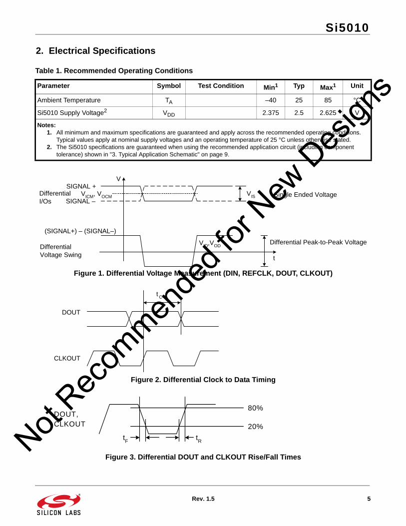
Figure 1. Differential Voltage Measurement (DIN, REFCLK, DOUT, CLKOUT)
Figure 2. Differential Clock to Data Timing
Figure 3. Differential DOUT and CLKOUT Rise/Fall Times
Table 1. Recommended Operating Conditions
Parameter Symbol Test Condition Min1 Typ Max1 Unit
Ambient Temperature TA –40 25 85 °C
Si5010 Supply Voltage2 VDD 2.375 2.5 2.625 V
Notes:1. All minimum and maximum specifications are guaranteed and apply across the recommended operating conditions.
Typical values apply at nominal supply voltages and an operating temperature of 25 °C unless otherwise stated.2. The Si5010 specifications are guaranteed when using the recommended application circuit (including component
tolerance) shown in "3. Typical Application Schematic" on page 9.
VIS
VID,VOD
DifferentialI/Os
DifferentialVoltage Swing
Differential Peak-to-Peak Voltage
SIGNAL +
SIGNAL –
(SIGNAL+) – (SIGNAL–)
VICM, VOCM
V
t
Single Ended Voltage
DOUT
t C-D
CLKOUT
DOUT,CLKOUT
tF tR
80%
20%
Not Rec
ommen
ded f
or New
Des
igns
Si5010
6 Rev. 1.5
Table 2. DC Characteristics(VDD = 2.5 V ±5%, TA = –40 to 85 °C)
Parameter Symbol Test Condition Min Typ Max Unit
Supply CurrentOC-12OC-3
IDD——
117124
131138
mA
Power DissipationOC-12OC-3
PD——
293310
344362
mW
Common Mode Input Voltage (DIN, REFCLK) VICM varies with VDD — .80 x VDD — V
Single Ended Input Voltage (DIN, REFCLK) VIS See Figure 1 200 — 750 mVPP
Differential Input Voltage Swing* (DIN, REFCLK)
VID See Figure 1 200 — 1500 mVPP
Input Impedance (DIN, REFCLK) RIN Line-to-Line 84 100 116
Output Short to GND (DOUT,CLKOUT) ISC(–) — 25 31 mA
Output Short to VDD (DOUT,CLKOUT) ISC(+) –17.5 –14.5 — mA
Input Voltage Low (LVTTL Inputs) VIL — — .8 V
Input Voltage High (LVTTL Inputs) VIH 2.0 — — V
Input Low Current (LVTTL Inputs) IIL — — 10 A
Input High Current (LVTTL Inputs) IIH — — 10 A
Output Voltage Low (LVTTL Outputs) VOL IO = 2 mA — — 0.4 V
Output Voltage High (LVTTL Outputs) VOH IO = 2 mA 2.0 — — V
Input Impedance (LVTTL Inputs) RIN 10 — — k
PWRDN/CAL Leakage Current IPWRDN VPWRDN 0.8 V 15 25 35 A
*Note: The DIN and REFCLK inputs may be driven differentially or single-endedly. When driving single-endedly, the voltage swing of the signal applied to the active input must exceed the specified minimum differential input voltage swing (VID min) and the unused input must be ac-coupled to ground. When driving differentially, the difference between the positive and negative input signals must exceed VID min. (Each individual input signal needs to swing only half of this range.) In either case, the voltage applied to any individual pin (DIN+, DIN–, REFCLK+, or REFCLK–) must not exceed the specified maximum Input Voltage Range (VIS max). Not Rec
ommen
ded f
or New
Des
igns
Si5010
Rev. 1.5 7
Table 3. AC Characteristics (Clock & Data)(VA 2.5 V ±5%, TA = –40 to 85 °C)
RMS Jitter Generation* JGEN(rms) with no jitter on serial data — 1.6 3.0 mUI
Peak-to-Peak Jitter Generation JGEN(PP) with no jitter on serial data — 25 55 mUI
Jitter Transfer Bandwidth* JBW OC-12 Mode — — 500 kHz
OC-3 Mode — — 130 kHz
Jitter Transfer Peaking* JP f < 2 MHz — .03 0.1 dB
Acquisition Time TAQ After falling edge of PWRDN/CAL
1.45 1.5 1.7 ms
From the return of valid data
40 60 150 s
Input Reference Clock Duty Cycle CDUTY 40 50 60 %
Reference Clock Range 19.44 155.52 MHz
Input Reference Clock Frequency Tolerance
CTOL –100 — 100 ppm
Frequency Difference at which Receive PLL goes out of Lock (REFCLK compared to the divided down VCO clock)
LOL 450 600 750 ppm
Frequency Difference at which Receive PLL goes into Lock (REFCLK compared to the divided down VCO clock)
LOCK 150 300 450 ppm
*Note: Bellcore specifications: GR-253-CORE, Issue 3, September 2000. Using PRBS 223 –1 data pattern.
Not Rec
ommen
ded f
or New
Des
igns
Si5010
8 Rev. 1.5
Table 5. Absolute Maximum Ratings
Parameter Symbol Value Unit
DC Supply Voltage VDD –0.5 to 2.8 V
LVTTL Input Voltage VDIG –0.3 to 3.6 V
Differential Input Voltages VDIF –0.3 to (VDD+ 0.3) V
Maximum Current any output PIN ±50 mA
Operating Junction Temperature TJCT –55 to 150 °C
Storage Temperature Range TSTG –55 to 150 °C
ESD HBM Tolerance (100 pf, 1.5 k) 1 kV
Note: Permanent device damage may occur if the above absolute maximum ratings are exceeded. Functional operation should be restricted to the conditions as specified in the operational sections of this data sheet. Exposure to absolute maximum rating conditions for extended periods may affect device reliability.
Table 6. Thermal Characteristics
Parameter Symbol Test Condition Value Unit
Thermal Resistance Junction to Ambient JA Still Air 38 °C/W
Not Rec
ommen
ded f
or New
Des
igns
Si5010
Rev. 1.5 9
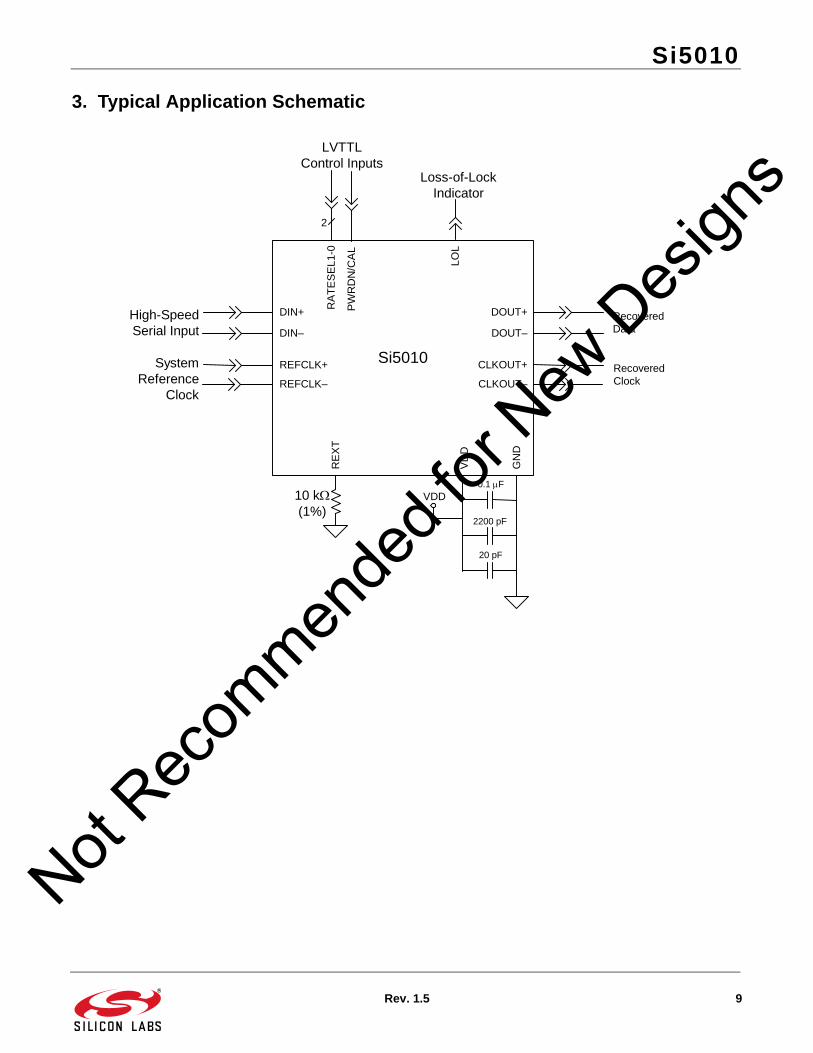
3. Typical Application Schematic
Si5010
LVTTLControl Inputs
Loss-of-LockIndicator
LOL
High-SpeedSerial Input
SystemReference
Clock
DIN+
DIN–
REFCLK+
REFCLK–
RE
XT
VD
D
GN
D
DOUT+
DOUT–
CLKOUT+
CLKOUT–
RecoveredData
RecoveredClock
0.1 F
2200 pF
VDD10 k(1%)
RA
TE
SE
L1-0
PW
RD
N/C
AL
2
20 pF
Not Rec
ommen
ded f
or New
Des
igns
Si5010
10 Rev. 1.5
4. Functional Description
The Si5010 utilizes a phase-locked loop (PLL) torecover a clock synchronous to the input data stream.This clock is used to retime the data, and both therecovered clock and data are output synchronously viacurrent mode logic (CML) drivers. Optimal jitterperformance is obtained by using Silicon Laboratories'DSPLL® technology to eliminate the noise entry pointscaused by external PLL filter components.
4.1. DSPLL®
The PLL structure (shown in "3. Typical ApplicationSchematic" on page 9) utilizes Silicon Laboratories'DSPLL technology to eliminate the need for externalloop filter components found in traditional PLLimplementations. This is achieved by using a digitalsignal processing (DSP) algorithm to replace the loopfilter commonly found in analog PLL designs. Thisalgorithm processes the phase detector error term andgenerates a digital control value to adjust the frequencyof the voltage-controlled oscillator (VCO). Becauseexternal loop filter components are not required,sensitive noise entry points are eliminated, thus makingthe DSPLL less susceptible to board-level noisesources that make SONET/SDH jitter compliancedifficult to attain.
4.2. PLL Self-CalibrationThe Si5020 achieves optimal jitter performance byusing self-calibration circuitry to set the loop gainparameters within the DSPLL. For the self-calibrationcircuitry to operate correctly, the power supply voltagemust exceed 2.25 V when calibration occurs. For bestperformance, the user should force a self-calibrationonce the supply has stabilized on power-up.
A self-calibration can be initiated by forcing a high-to-low transition on the power-down control input,PWRDN/CAL, while a valid reference clock is suppliedto the REFCLK input. The PWRDN/CAL input should beheld high at least 1 s before transitioning low toguarantee a self-calibration. Several application circuitsthat could be used to initiate a power-on self-calibrationare provided in Silicon Laboratories application note“AN42: Controlling DSPLL Self-Calibration for theSi5020/5018/5010 CDR Devices and Si531x ClockMultiplier/Regenerator Devices”.
4.3. Multi-Rate OperationThe Si5010 supports clock and data recovery for OC-12/3 and STM-4/1 data streams.
Multi-rate operation is achieved by configuring thedevice to divide down the output of the VCO to thedesired data rate. The RATESEL configuration andassociated data rates are given in Table 7.
4.4. Reference Clock DetectThe Si5010 CDR requires an external reference clockapplied to the REFCLK input for normal deviceoperation. When REFCLK is absent, the LOL alarm willalways be asserted when it has been determined thatno activity exists on REFCLK, indicating the lock statusof the PLL is unknown. Additionally, the Si5010 uses thereference clock to center the VCO operating frequencyso that clock and data can be recovered from the inputdata stream. The VCO operates at an integer multiple ofthe REFCLK frequency. (See “Lock Detect” section.)The device will self configure for operation with one ofthree reference clock frequencies. This eliminates theneed to externally configure the device to operate with aparticular reference clock. The REFCLK frequencyshould be 19.44 MHz, 77.76 MHz, or 155.52 MHz with afrequency accuracy of ±100 ppm.
4.5. Lock DetectThe Si5010 provides lock-detect circuitry that indicateswhether the PLL has achieved frequency lock with theincoming data. The circuit compares the frequency of adivided-down version of the recovered clock with thefrequency of the applied reference clock (REFCLK). Ifthe recovered clock frequency deviates from that of thereference clock by the amount specified in Table 4 onpage 7, the PLL is declared out-of-lock, and the loss-of-lock (LOL) pin is asserted high. In this state, the PLL willperiodically try to reacquire lock with the incoming datastream. During reacquisition, the recovered clock maydrift over a ±600 ppm range relative to the appliedreference clock, and the LOL output alarm may toggleuntil the PLL has reacquired frequency lock. Due to thelow noise and stability of the DSPLL, under thecondition where data is removed from the inputs, thereis the possibility that the PLL will not drift enough torender an out-of-lock condition.
Table 7. Data-Rate Configuration
RATESEL SONET/SDH
0 622.08 Mbps
1 155.52 Mbps
Not Rec
ommen
ded f
or New
Des
igns
Si5010
Rev. 1.5 11
If REFCLK is removed, the LOL output alarm will alwaysbe asserted when it has been determined that noactivity exists on REFCLK, indicating the frequency lockstatus of the PLL is unknown.
Note: LOL is not asserted during PWRDN/CAL.
4.6. PLL PerformanceThe PLL implementation used in the Si5010 is fullycompliant with the jitter specifications proposed forSONET/SDH equipment by Bellcore GR-253-CORE,Issue 3, September 2000 and ITU-T G.958.
4.6.1. Jitter Tolerance
The Si5010’s tolerance to input jitter exceeds that of theBellcore/ITU mask shown in Figure 4. This maskdefines the level of peak-to-peak sinusoid jitter thatmust be tolerated when applied to the differential datainput of the device.
Figure 4. Jitter Tolerance Specification
4.6.2. Jitter Transfer
The Si5010 is fully compliant with the relevant Bellcore/ITU specifications related to SONET/SDH jitter transfer.Jitter transfer is defined as the ratio of output signal jitterto input signal jitter as a function of jitter frequency (seeFigure 5). These measurements are made with an inputtest signal that is degraded with sinusoidal jitter whosemagnitude is defined by the mask in Figure 4.
4.6.3. Jitter Generation
The Si5010 meets all relevant specifications for jittergeneration proposed for SONET/SDH equipment. Thejitter generation specification defines the amount of jitterthat may be present on the recovered clock and dataoutputs when a jitter free input signal is provided. TheSi5010 typically generates less than 1.6 mUIrms of jitterwhen presented with jitter-free input data.
Figure 5. Jitter Transfer Specification
4.7. PowerdownThe Si5010 provides a powerdown pin, PWRDN/CAL,that disables the device. When the PWRDN/CAL pin isdriven high, the positive and negative terminals ofCLKOUT and DOUT are each tied to VDD through100 on-chip resistors. This feature is useful inreducing power consumption in applications thatemploy redundant serial channels. When PWRDN/CALis released (set to low) the digital logic resets to aknown initial condition, recalibrates the DSPLL®, andwill begin to lock to the data stream.
Note: LOL is not asserted when the device is in the power-down state.
4.8. Device GroundingThe Si5010 uses the GND pad on the bottom of the 20-pin QFN package for device ground. This pad should beconnected directly to the analog supply ground. SeeFigures 10 and 12 for the ground (GND) pad location.
f0 f1 f2 f3 ft
Frequency
0.15
1.5
15
SinusoidalInput
Jitter (UI p-p)Slope = 20 dB/Decade
SONETData Rate
F0(Hz)
F1(Hz)
F2(Hz)
F3(kHz)
Ft(kHz)
OC-12
OC-3
10
10
30
30
300
300
25
6.5
250
65
FcFrequency
JitterTransfer
0.1 dB
AcceptableRange
20 dB/DecadeSlope
SONETData Rate
OC-12
OC-3
Fc(kHz)
500
130
Not Rec
ommen
ded f
or New
Des
igns
Si5010
12 Rev. 1.5
4.9. Bias Generation CircuitryThe Si5010 makes use of an external resistor to setinternal bias currents. The external resistor allowsprecise generation of bias currents which significantlyreduces power consumption versus traditionalimplementations that use an internal resistor. The biasgeneration circuitry requires a 10 k (1%) resistorconnected between REXT and GND.
4.10. Differential Input CircuitryThe Si5010 provides differential inputs for both the high-speed data (DIN) and the reference clock (REFCLK)inputs. An example termination for these inputs isshown in Figure 6. In applications where direct dccoupling is possible, the 0.1 µF capacitors may beomitted. The DIN and REFCLK input amplifiers requirean input signal with a minimum differential peak-to-peakvoltage listed in Table 2 on page 6.
Figure 6. Input Termination for DIN and REFCLK (AC-coupled)
Figure 7. Single-Ended Input Termination for REFCLK (AC-coupled)
Differential Driver
Si5010
0.1 µF Zo = 50
Zo = 50
DIN+,REFCLK+
DIN–,REFCLK–
2.5 k
2.5 k10 k
10 k
102
VDD
GND
0.1 µF
0.1 F
Clocksource
Si5010
0.1 F Zo = 50 REFCLK +
REFCLK –
2.5 k
2.5 k10 k
10 k
100
GND
VDD
102
Not Rec
ommen
ded f
or New
Des
igns
Si5010
Rev. 1.5 13
Figure 8. Single-Ended Input Termination for DIN (AC-coupled)
4.11. Differential Output CircuitryThe Si5010 utilizes a current mode logic (CML)architecture to output both the recovered clock(CLKOUT) and data (DOUT). An example of outputtermination with ac coupling is shown in Figure 9. In
applications in which direct dc coupling is possible, the0.1 µF capacitors may be omitted. The differential peak-to-peak voltage swing of the CML architecture is listedin Table 2 on page 6.
Figure 9. Output Termination for DOUT and CLKOUT (AC-coupled)
0.1 F
Clocksource
Si5010
0.1 F Zo = 50 DIN +
DIN –
2.5 k
2.5 k10 k
10 k
100
GND
VDD
102
DOUT–,CLKOUT–
50
50
0.1 F
0.1 F
Zo = 50
Zo = 50
Si5010 VDD
VDD
100
100
VDD
VDD
DOUT+,CLKOUT+
Not Rec
ommen
ded f
or New
Des
igns
Si5010
14 Rev. 1.5
5. Pin Descriptions: Si5010
Figure 10. Si5010 Pin Configuration
Table 8. Si5010 Pin Descriptions
Pin # Pin Name I/O Signal Level Description
1 REXT External Bias Resistor.
This resistor is used by onboard circuitry to estab-lish bias currents within the device. This pin must be connected to GND through a 10 k1resis-tor.
2, 7, 11, 14 VDD 2.5 V Supply Voltage.
Nominally 2.5 V.
3, 8, 18, and GND Pad
GND GND Supply Ground.
Nominally 0.0 V. The GND pad found on the bottom of the 20-pin micro leaded package (see Figure 12) must be connected directly to supply ground.
45
REFCLK+REFCLK–
I See Table 2 Differential Reference Clock.
The reference clock sets the initial operating fre-quency used by the onboard PLL for clock and data recovery. Additionally, the reference clock is used to derive the clock output when no data is present.
6 LOL O LVTTL Loss-of-Lock.
This output is driven high when the recovered clock frequency deviates from the reference clock by the amount specified in Table 4 on page 7.
910
DIN+DIN–
I See Table 2 Differential Data Input.
Clock and data are recovered from the differential signal present on these pins.
GNDPad
Connection
15
14
13
12
11
PWRDN/CAL
DOUT+
VDD
DOUT–
VDD
1
2
3
4
5
VDD
GND
REFCLK–
REXT
REFCLK+
20 19 18 17 16
NC
RA
TE
SE
L
CL
KO
UT
–
CL
KO
UT
+
GN
D
6 7 8 9 10
LO
L
GN
D
DIN
+
DIN
–
VD
D
Top View
Not Rec
ommen
ded f
or New
Des
igns
Si5010
Rev. 1.5 15
1213
DOUT–DOUT+
O CML Differential Data Output.
The data output signal is a retimed version of the data recovered from the signal present on DIN. It is phase aligned with CLKOUT and is updated on the rising edge of CLKOUT.
15 PWRDN/CAL I LVTTL Powerdown.
To shut down the high-speed outputs and reduce power consumption, hold this pin high. For normal operation, hold this pin low. Calibration.
To initiate an internal self-calibration, force a high-to-low transition on this pin. (See "4.2. PLL Self-Calibration" on page 10.) Note: This input has a weak internal pulldown.
1617
CLKOUT–CLKOUT+
O CML Differential Clock Output.
The output clock is recovered from the data signal present on DIN. In the absence of data, the output clock is derived from REFCLK.
19 RATESEL I LVTTL Data Rate Select.
This pin configures the onboard PLL for clock and data recovery at one of two user selectable data rates. See Table 7 for configuration settings.Note: This input has a weak internal pulldown.
20 NC No Connect.
This pin should be tied to ground.
Table 8. Si5010 Pin Descriptions (Continued)
Pin # Pin Name I/O Signal Level Description
Not Rec
ommen
ded f
or New
Des
igns
Si5010
16 Rev. 1.5
6. Ordering Guide
Part Number Package Voltage Pb-Free Temperature
Si5010-X-GM 20-lead QFN 2.5 Yes –40 to 85 °C
Notes:1. “X” denotes product revision.2. Add an “R” at the end of the device to denote tape and reel option; 2500 quantity per reel.3. These devices use a NiPdAu pre-plated finish on the leads that is fully RoHS6 compliant while being
fully compatible with both leaded and lead-free card assembly processes.
Not Rec
ommen
ded f
or New
Des
igns
Si5010
Rev. 1.5 17
7. Top Marking
Figure 11. Si5010 Top Marking
Table 9. Top Marking Explanation
Part Number Die Revision (R) Assembly Date (YWW)
Si5010-B-GM B Y = Last digit of current yearWW = Work week
Not Rec
ommen
ded f
or New
Des
igns
Si5010
18 Rev. 1.5
8. Package Outline
Figure 12 illustrates the package details for the Si5010. Table 10 lists the values for the dimensions shown in theillustration.
Figure 12. 20-pin Quad Flat No-Lead (QFN)
Table 10. Package Dimensions
Dimension Min Nom Max Dimension Min Nom Max
A 0.80 0.85 0.90 E2 2.0 2.10 2.20
A1 0.00 0.02 0.05 L 0.50 0.60 0.70
b 0.18 0.25 0.30 aaa 0.15
D 4.00 BSC bbb 0.10
D2 2.0 2.10 2.20 ccc 0.08
e 0.50 BSC ddd 0.05
E 4.00 BSC eee 0.05
Notes:1. All dimensions shown are in millimeters (mm) unless otherwise noted.2. Dimensioning and Tolerancing per ANSI Y14.5M-1994.3. This drawing conforms to JEDEC outline MO-220, variation VGGD-1.4. Recommended card reflow profile is per the JEDEC/IPC J-STD-020C specification for Small Body Components.
Not Rec
ommen
ded f
or New
Des
igns
9. 4x4 mm 20L QFN Recommended PCB Layout
Figure 13. 4x4 mm 20L QFN PCB Layout
Table 11. PCB Land Pattern Dimensions
Symbol Parameter Dimensions
Min Nom Max
A Pad Row/Column Width/Length 2.23 2.25 2.28
D Thermal Pad Width/Height 2.03 2.08 2.13
e Pad Pitch — 0.50 BSC —
G Pad Row/Column Separation 2.43 2.46 2.48
R Pad Radius — 0.12 REF —
Notes:1. All dimensions listed are in millimeters (mm).2. The perimeter pads are to be Non-Solder Mask Defined (NSMD). Solder mask openings should be designed to leave 60-75 mm
separation between solder mask and pad metal, all the way around the pad.3. The center thermal pad is to be Solder Mask Defined (SMD).4. Thermal/Ground vias placed in the center pad should be no less than 0.2 mm (8 mil) diameter and tented from the top to prevent
solder from flowing into the via hole.5. The stencil aperture should match the pad size (1:1 ratio) for the perimeter pads. A 3x3 array of 0.5 mm square stencil openings, on a
0.65 mm pitch, should be used for the center thermal pad.6. A stencil thickness of 5 mil is recommended. The stencil should be laser cut and electropolished, with trapezoidal walls to facilitate
paste release.7. A “No-Clean”, Type 3 solder paste should be used for assembly. Nitrogen purge during reflow is recommended.8. Do not place any signal or power plane vias in these “keep out” regions.9. Suggest four 0.38 mm (15 mil) vias to the ground plane.
See Note 8
Gnd
Pin
Gnd Pin
Gn
d P
in
See Note 9
Not Rec
ommen
ded f
or New
Des
igns
Si5010
20 Rev. 1.5
X Pad Width 0.23 0.25 0.28
Y Pad Length — 0.94 REF —
Z Pad Row/Column Extents 4.26 4.28 4.31
Table 11. PCB Land Pattern Dimensions (Continued)
Notes:1. All dimensions listed are in millimeters (mm).2. The perimeter pads are to be Non-Solder Mask Defined (NSMD). Solder mask openings should be designed to leave 60-75 mm
separation between solder mask and pad metal, all the way around the pad.3. The center thermal pad is to be Solder Mask Defined (SMD).4. Thermal/Ground vias placed in the center pad should be no less than 0.2 mm (8 mil) diameter and tented from the top to prevent
solder from flowing into the via hole.5. The stencil aperture should match the pad size (1:1 ratio) for the perimeter pads. A 3x3 array of 0.5 mm square stencil openings, on a
0.65 mm pitch, should be used for the center thermal pad.6. A stencil thickness of 5 mil is recommended. The stencil should be laser cut and electropolished, with trapezoidal walls to facilitate
paste release.7. A “No-Clean”, Type 3 solder paste should be used for assembly. Nitrogen purge during reflow is recommended.8. Do not place any signal or power plane vias in these “keep out” regions.9. Suggest four 0.38 mm (15 mil) vias to the ground plane.
Not Rec
ommen
ded f
or New
Des
igns
Si5010
Rev. 1.5 21
DOCUMENT CHANGE LIST
Revision 1.0 to Revision 1.1Added "7. Top Marking" on page 17.
Updated “8. Package Outline: Si5010-BM” on page 17.
Added "9. 4x4 mm 20L QFN Recommended PCB Layout" on page 19.
Revision 1.1 to Revision 1.2Made minor note corrections to "9. 4x4 mm 20L
QFN Recommended PCB Layout" on page 19.
Revision 1.2 to Revision 1.3Global change: MLP to QFN.
Updated "6. Ordering Guide" on page 16.
Updated "7. Top Marking" on page 17.
Updated "8. Package Outline" on page 18.
Updated "9. 4x4 mm 20L QFN Recommended PCB Layout" on page 19.
Revision 1.3 to Revision 1.4Changed Minimum Output Clock Rate to
150 MHz in Table 3 on page 7.
Added "7. Top Marking" on page 17.
Updated "6. Ordering Guide" on page 16.
Updated "8. Package Outline" on page 18.
Revision 1.4 to Revision 1.5Updated “8. Package Outline”
Not Rec
ommen
ded f
or New
Des
igns
DisclaimerSilicon Laboratories intends to provide customers with the latest, accurate, and in-depth documentation of all peripherals and modules available for system and software implementers using or intending to use the Silicon Laboratories products. Characterization data, available modules and peripherals, memory sizes and memory addresses refer to each specific device, and "Typical" parameters provided can and do vary in different applications. Application examples described herein are for illustrative purposes only. Silicon Laboratories reserves the right to make changes without further notice and limitation to product information, specifications, and descriptions herein, and does not give warranties as to the accuracy or completeness of the included information. Silicon Laboratories shall have no liability for the consequences of use of the information supplied herein. This document does not imply or express copyright licenses granted hereunder to design or fabricate any integrated circuits. The products must not be used within any Life Support System without the specific written consent of Silicon Laboratories. A "Life Support System" is any product or system intended to support or sustain life and/or health, which, if it fails, can be reasonably expected to result in significant personal injury or death. Silicon Laboratories products are generally not intended for military applications. Silicon Laboratories products shall under no circumstances be used in weapons of mass destruction including (but not limited to) nuclear, biological or chemical weapons, or missiles capable of delivering such weapons.
Trademark InformationSilicon Laboratories Inc., Silicon Laboratories, Silicon Labs, SiLabs and the Silicon Labs logo, CMEMS®, EFM, EFM32, EFR, Energy Micro, Energy Micro logo and combinations thereof, "the world’s most energy friendly microcontrollers", Ember®, EZLink®, EZMac®, EZRadio®, EZRadioPRO®, DSPLL®, ISOmodem ®, Precision32®, ProSLIC®, SiPHY®, USBXpress® and others are trademarks or registered trademarks of Silicon Laboratories Inc. ARM, CORTEX, Cortex-M3 and THUMB are trademarks or registered trademarks of ARM Holdings. Keil is a registered trademark of ARM Limited. All other products or brand names mentioned herein are trademarks of their respective holders.
http://www.silabs.com
Silicon Laboratories Inc.400 West Cesar ChavezAustin, TX 78701USA
ClockBuilder Pro
One-click access to Timing tools, documentation, software, source code libraries & more. Available for Windows and iOS (CBGo only).


![TITLE PAGE SHEET02 - support.spectrumdigital.comsupport.spectrumdigital.com/boards/evmomapl137/revd/files/EVMOMAPL...DIN: AXR1[5] (McASP) DOUT: AXR1[0] (McASP) Drive the MCLK into](https://static.documents.pub/doc/80x56/5ab134327f8b9abc2f8c628c/title-page-sheet02-axr15-mcasp-dout-axr10-mcasp-drive-the-mclk-into-mcasp1.jpg)


