125
OMSE 510: Computing Foundations 2: Disks, Buses, DRAM Portland State University/OMSE
| Date post: | 20-Dec-2015 |
| Category: |
Documents |
| View: | 216 times |
| Download: | 0 times |

OMSE 510: Computing Foundations2: Disks, Buses, DRAM
Portland State University/OMSE

Outline of Comp. ArchitectureOutline of the rest of the computer architecture
section:
Start with a description of computer devices, work back towards the CPU.

Computer Architecture Is …
the attributes of a [computing] system as seen by the programmer, i.e., the conceptual structure and functional behavior, as distinct from the organization of the data flows and controls the logic design, and the physical implementation.
Amdahl, Blaaw, and Brooks, 1964
SOFTWARESOFTWARE

Today
Begin Computer Architecture
Disk Drives
The Bus
Memory
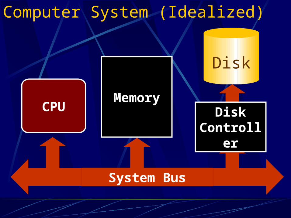
Computer System (Idealized)
CPUMemory
System Bus
Disk Controller
Disk

I/O Device Examples
Device Behavior Partner Data Rate (KB/sec)
Keyboard Input Human 0.01
Mouse Input Human 0.02
Line Printer Output Human 1.00
Floppy disk Storage Machine 50.00
Laser Printer Output Human 100.00
Optical Disk Storage Machine 500.00
Magnetic Disk Storage Machine 5,000.00
Network-LAN Input or Output Machine 20 – 1,000.00
Graphics Display Output Human 30,000.00

A Device: The Disk
Disk Drives!
- eg. Your hard disk drive
- Where files are physically stored
- Long-term non-volatile storage device
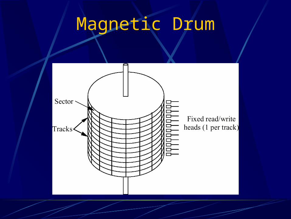
Magnetic Drum

Spiral Format for Compact Disk

A Device: The DiskMagnetic Disks
- Your hard disk drive
- Where files are physically stored
- Long-term non-volatile storage device

A Magnetic Disk with Three Platters

Organization of a Disk Platter with a 1:2 Interleave Factor

Disk Physical Characteristics
Platters 1 to 20 with diameters from 1.3 to 8 inches (Recording
on both sides)
Tracks 2500 to 5000 Tracks/inch
Cylinders all tracks in the same position in the platters
Sectors 128-256 sectors/track with gaps and info related to
sectors between them (typical sector, 256-512 bytes)

Disk Physical Characteristics
Trend as of 2005:
Constant bit density (105 bits/inch) Ie. More info (sectors) on outer tracks
Strangely enough, history reverses itself Originally, disks were constant bit density (more
efficient) Then, went to uniform #sectors/track (simpler, allowed
easier optimization) Returning now to constant bit density
Disk capacity follows Moore’s law: doubles every 18 months

Example: Seagate Barracuda
Disk for server
10 disks hence 20 surfaces
7500 cylinders, hence 7500*20 = 150000 total tracks
237 sectors/track (average)
512 bytes/sector
Total capacity:
150000 * 237 * 512 = 18,201,600,000 bytes
= 18 GB

Things to consider
Addressing modes: Computers always refer to data in blocks (512bytes
common) How to address blocks? Old school: CHS (Cylinder-Head-Sector)
Computer has an idea how the drive is structured
New School: LBA (Large Block Addressing) Linear!

Disk Performance
Steps to read from disk:
1. CPU tells drive controller “need data from this address”
2. Drive decodes instruction
3. Move read head over desired cylinder/track (seek)
4. Wait for desired sector to rotate under read head
5. Read the data as it goes under drive head

Disk Performance
Components of disk performance:
Seek time (to move the arm on the right cylinder)
Rotation time (on average ½ rotation) (time to find the right sector)
Transfer time depends on rotation time
Disk controller time. Overhead to perform an access

Disk Performance
So Disk Latency = Queuing Time + Controller time + Seek time + Rotation time + Transfer time

Seek Time
From 0 (if arm already positioned) to a maximum 15-20 ms
Note: This is not a linear function of distance (speedup + coast + slowdown + settle)
Even when reading tracks on the same cylinder, there is a minimal seek time (due to severe tolerances for head positioning)
Barracuda example: Average seek time = 8 ms, track to track seek time = 1 ms, full disk seek = 17ms

Rotation time
Rotation time:
Seagate Barracuda: 7200 RPM
(Disks these days are 3600, 4800, 5400, 7200 up to 10800 RPM)
7200 RPM = 120 RPS = 8.33ms per rotation
Average rotational latency = ½ worst case rotational latency = 4.17ms

Transfer time
Transfer time depends on rotation time, amount of data to transfer (minimum one sector), recording density, disk/memory connection
These days, transfer time around 2MB/s to 16MB/s
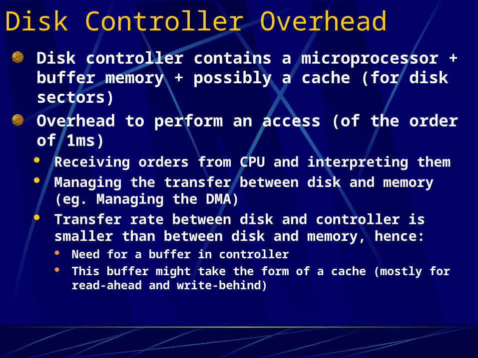
Disk Controller OverheadDisk controller contains a microprocessor + buffer memory + possibly a cache (for disk sectors)
Overhead to perform an access (of the order of 1ms) Receiving orders from CPU and interpreting them Managing the transfer between disk and memory (eg.
Managing the DMA) Transfer rate between disk and controller is smaller
than between disk and memory, hence: Need for a buffer in controller This buffer might take the form of a cache (mostly for read-
ahead and write-behind)

Disk Time ExampleDisk Parameters: Transfer size is 8K bytes Advertised average seek is 12 ms Disk spins at 7200 RPM Transfer rate is 4MB/s
Controller overhead is 2ms
Assume disk is idle so no queuing delay
What is Average disk time for a sector?avg seek + avg rot delay + transfer time + controller
overhead
____ + _____ + _____ + _____

Disk Time ExampleAnswer: 20ms
But! Advertised seek time assumes no locality: typically ¼ to 1/3rd advertised seek time!
20ms->12ms
Locality is an effect of smart placement of data by the operating system

My DiskHitachi Travelstar 7K100 60GB ATA-6 2.5in
7200RPM Mobile Hard Drive w/8MB Buffer Interface:
ATA-6 Capacity (GB)1: 60 Sector size (bytes): 512 Data heads: 3 Disks: 2
Performance
Data buffer (MB): 8 Rotational speed (rpm): 7,200 Latency (average ms): 4.2 Media transfer rate (Mbits/sec): 561 Max.interface transfer rate (MB/sec): 100 Ultra DMA mode-5 16.6 PIO mode-4Command Overhead: 1ms
Seek time (ms): Average: 10 R / 11 W Track to track: 1 R / 1.2 W Full stroke:18 R / 19 W
Sectors per Track: 414-792Max.areal density (Gbits/sq.inch): 66
Disk to buffer data transfer: 267-629 Mb/s
Buffer-host data transfer: 100 MB/s

Some other quotesHard Drives:
Notebook: Toshiba MK8026GAX 80GB, 2.5", 9.5mm, 5400 RPM, 12ms seek, 100MB/s
Desktop: Seagate 250GB, 7200RPM, SATA II, 9-11ms seek
Buffer to host: 300MB/s
Buffer to disk: 93MB/s
Server: Seagate Raptor SATA, 10000RPM, SATA
Buffer to host: 150MB/s
Buffer to disk: 72MB/s

Next Topic
Disk Arrays
RAID!

Disk Capacity now doubles every 18 months; before1990 every 36 months
• Today: Processing Power Doubles Every 18 months
• Today: Memory Size Doubles Every 18 months(4X/3yr)
• Today: Disk Capacity Doubles Every 18 months
• Disk Positioning Rate (Seek + Rotate) Doubles Every Ten Years!
• Caches in Memory and Device Controllers to Close the Gap
The I/OGAP
The I/OGAP
Technology Trends

14”10”5.25”3.5”
3.5”
Disk Array: 1 disk design
Conventional: 4 disk designs
Low End High End
Disk Product Families
Manufacturing Advantages of Disk Arrays

Data Capacity
Volume
Power
Data Rate
I/O Rate
MTTF
Cost
IBM 3390 (K)
20 GBytes
97 cu. ft.
3 KW
15 MB/s
600 I/Os/s
250 KHrs
$250K
IBM 3.5" 0061
320 MBytes
0.1 cu. ft.
11 W
1.5 MB/s
55 I/Os/s
50 KHrs
$2K
3.5”x70
23 GBytes
11 cu. ft.
1 KW
120 MB/s
3900 IOs/s
??? Hrs
$150K
Disk Arrays have potential for
large data and I/O rates
high MB per cu. ft., high MB per KW
reliability?
Small # of Large Disks Large # of Small Disks!

• Reliability of N disks = Reliability of 1 Disk ÷ N
50,000 Hours ÷ 70 disks = 700 hours
Disk system MTTF: Drops from 6 years to 1 month!
• Arrays (without redundancy) too unreliable to be useful!
Hot spares support reconstruction in parallel with access: very high media availability can be achievedHot spares support reconstruction in parallel with access: very high media availability can be achieved
Array Reliability

Media Bandwidth/Latency Demands
Bandwidth requirements High quality video
Digital data = (30 frames/s) × (640 x 480 pixels) × (24-b color/pixel) = 221 Mb/s (27.625 MB/s)
High quality audio Digital data = (44,100 audio samples/s) × (16-b audio samples) ×
(2 audio channels for stereo) = 1.4 Mb/s (0.175 MB/s) Compression reduces the bandwidth requirements considerably
Latency issues How sensitive is your eye (ear) to variations in video (audio) rates? How can you ensure a constant rate of delivery? How important is synchronizing the audio and video streams?
15 to 20 ms early to 30 to 40 ms late tolerable

Dependability, Reliability, Availability
Reliability – a measure of the reliability measured by the mean time to failure (MTTF). Service interruption is measured by mean time to repair (MTTR)
Availability – a measure of service accomplishment
Availability = MTTF/(MTTF + MTTR)
To increase MTTF, either improve the quality of the components or design the system to continue operating in the presence of faulty components
1. Fault avoidance: preventing fault occurrence by construction
2. Fault tolerance: using redundancy to correct or bypass faulty components (hardware)
Fault detection versus fault correction Permanent faults versus transient faults

RAIDs: Disk Arrays
Arrays of small and inexpensive disks Increase potential throughput by having many disk drives
Data is spread over multiple disks Multiple accesses are made to several disks at a time
Reliability is lower than a single disk
But availability can be improved by adding redundant disks (RAID) Lost information can be reconstructed from redundant information MTTR: mean time to repair is in the order of hours MTTF: mean time to failure of disks is tens of years
Redundant Array of Inexpensive Disks

RAID: Level 0 (No Redundancy; Striping)
Multiple smaller disks as opposed to one big disk Spreading the data over multiple disks – striping – forces
accesses to several disks in parallel increasing the performance
Four times the throughput for a 4 disk system
Same cost as one big disk – assuming 4 small disks cost the same as one big disk
No redundancy, so what if one disk fails? Failure of one or more disks is more likely as the number
of disks in the system increases
S0,b0 S0,b2S0,b1 S0,b3
sector numberbit number

RAID: Level 1 (Redundancy via Mirroring)
Uses twice as many disks as RAID 0 (e.g., 8 smaller disks with second set of 4 duplicating the first set) so there are always two copies of the data Still four times the throughput # redundant disks = # of data disks so twice the cost of
one big disk writes have to be made to both sets of disks, so writes would be
only 1/2 the performance of RAID 0
What if one disk fails? If a disk fails, the system just goes to the “mirror” for the
data
S0,b0 S0,b2S0,b1 S0,b3 S0,b0 S0,b1 S0,b2 S0,b3
redundant (check) data

RAID: Level 2 (Redundancy via ECC)
ECC disks contain the parity of data on a set of distinct overlapping disks Still four times the throughput # redundant disks = log (total # of disks) so almost twice
the cost of one big disk writes require computing parity to write to the ECC disks reads require reading ECC disk and confirming parity
Can tolerate limited disk failure, since the data can be reconstructed
S0,b0 S0,b2S0,b1 S0,b3
3 5 6 7 4 2 1
10 0 0 11
ECC disks
0
ECC disks 4 and 2 point to either data disk 6 or 7, but ECC disk 1 says disk 7 is okay, so disk 6 must be in error
1

RAID: Level 3 (Bit-Interleaved Parity)
Cost of higher availability is reduced to 1/N where N is the number of disks in a protection group Still four times the throughput # redundant disks = 1 × # of protection groups
writes require writing the new data to the data disk as well as computing the parity, meaning reading the other disks, so that the parity disk can be updated
Can tolerate limited disk failure, since the data can be reconstructed
reads require reading all the operational data disks as well as the parity disk to calculate the missing data that was stored on the failed disk
S0,b0 S0,b2S0,b1 S0,b3
10 0 1
parity diskdisk fails
1
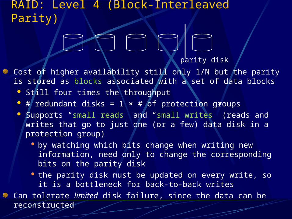
RAID: Level 4 (Block-Interleaved Parity)
Cost of higher availability still only 1/N but the parity is stored as blocks associated with a set of data blocks Still four times the throughput # redundant disks = 1 × # of protection groups Supports “small reads” and “small writes” (reads and writes that go to
just one (or a few) data disk in a protection group) by watching which bits change when writing new information, need
only to change the corresponding bits on the parity disk the parity disk must be updated on every write, so it is a bottleneck
for back-to-back writes
Can tolerate limited disk failure, since the data can be reconstructed
parity disk

Block WritesNew data
D0 D1 D2 D3 P
D0 D1 D2 D3 P
5 writes
involving all the disks
RAID 4 small writesNew data
D0 D1 D2 D3 P
D0 D1 D2 D3 P
2 reads and 2 writes
involving just two disks
RAID 3 block writes

RAID: Level 5 (Distributed Block-Interleaved Parity)
Cost of higher availability still only 1/N but the parity is spread throughout all the disks so there is no single bottleneck for writes Still four times the throughput # redundant disks = 1 × # of protection groups Supports “small reads” and “small writes” (reads and writes
that go to just one (or a few) data disk in a protection group) Allows multiple simultaneous writes as long as the
accompanying parity blocks are not located on the same disk
Can tolerate limited disk failure, since the data can be reconstructed

D0 D1 D2 D3 PD0'
+
+
D0' D1 D2 D3 P'
newdata
olddata
old parity
XOR
XOR
(1. Read) (2. Read)
(3. Write) (4. Write)
RAID-5: Small Write Algorithm
1 Logical Write = 2 Physical Reads + 2 Physical Writes
Problems of Disk Arrays: Block Writes

Distributing Parity Blocks
0 1 2 3 P0
4 5 6 7 P1
8 9 10 11 P2
12 13 14 15 P3
RAID 4 RAID 5
0 1 2 3 P0
4 5 6 P1 7
8 9 P2 10 11
12 P3 13 14 15
By distributing parity blocks to all disks, some small writes can be performed in parallel

Disks SummaryFour components of disk access time: Seek Time: advertised to be 3 to 14 ms but lower in real systems Rotational Latency: 5.6 ms at 5400 RPM and 2.0 ms at 15000 RPM Transfer Time: 10 to 80 MB/s Controller Time: typically less than .2 ms
RAIDS can be used to improve availability RAID 0 and RAID 5 – widely used in servers, one estimate is that 80% of disks
in servers are RAIDs RAID 1 (mirroring) – EMC, Tandem, IBM RAID 3 – Storage Concepts RAID 4 – Network Appliance
RAIDS have enough redundancy to allow continuous operation

Computer System (Idealized)
CPUMemory
System Bus
Disk Controller
Disk

Next Topic
Buses

Control
Datapath
Memory
ProcessorInput
Output
What is a bus?A Bus Is:
shared communication link
single set of wires used to connect multiple subsystems
A Bus is also a fundamental tool for composing large, complex systems systematic means of abstraction

Bridge Based Bus
Arch-itecture
Bridging with dual Pentium II Xeon processors on Slot 2.
(Source: http://www.intel.com.)

Buses

MemoryProcesser
I/O Device
I/O Device
I/O Device
Advantages of Buses
Versatility:New devices can be added easilyPeripherals can be moved between computersystems that use the same bus standard
Low Cost:A single set of wires is shared in multiple ways
MemoryProcesser
I/O Device
I/O Device
I/O Device
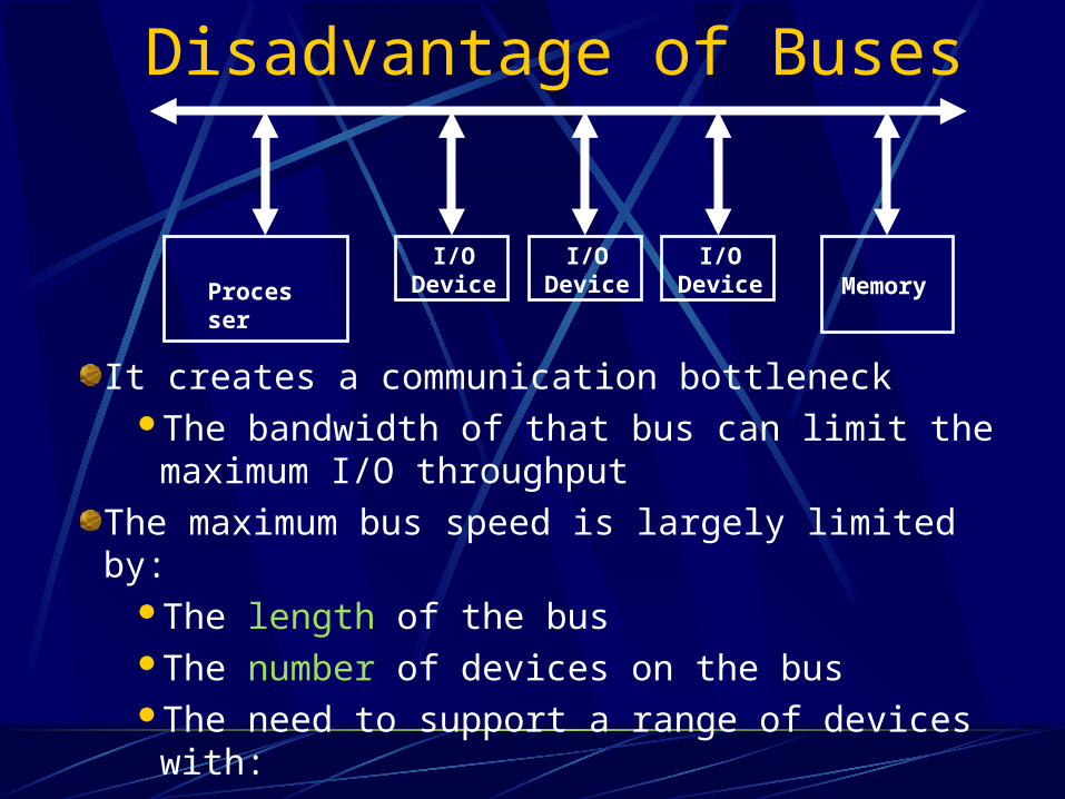
Disadvantage of Buses
It creates a communication bottleneckThe bandwidth of that bus can limit the maximum I/O
throughput
The maximum bus speed is largely limited by:The length of the busThe number of devices on the busThe need to support a range of devices with:
Widely varying latencies Widely varying data transfer rates

Data Lines
Control Lines
The General Organization of a Bus
Control lines:Signal requests and acknowledgmentsIndicate what type of information is on the data lines
Data lines carry information between the source and the destination:
Data and AddressesComplex commands

BusMaster
BusSlave
Master issues command
Data can go either way
Master versus Slave
A bus transaction includes two parts:Issuing the command (and address) – requestTransferring the data – action
Master is the one who starts the bus transaction by:issuing the command (and address)
Slave is the one who responds to the address by:Sending data to the master if the master ask for dataReceiving data from the master if the master wants to
send data

Types of BusesProcessor-Memory Bus (design specific)
Short and high speedOnly need to match the memory system
Maximize memory-to-processor bandwidthConnects directly to the processorOptimized for cache block transfers
I/O Bus (industry standard)Usually is lengthy and slowerNeed to match a wide range of I/O devicesConnects to the processor-memory bus or backplane bus
Backplane Bus (standard or proprietary)Backplane: an interconnection structure within the chassisAllow processors, memory, and I/O devices to coexistCost advantage: one bus for all components

Processor/MemoryBus -- Design Specific
Backplane Bus – PCIPCI Devices: Graphics IO Control
I/O Busses – IDE, USB & SCSI
Example: Pentium System Organization

Standard Intel Pentium Read and Write Bus Cycles

Intel Pentium Burst Read Bus Cycle

A Computer System with One Bus: Backplane Bus
Processor Memory
I/O Devices
Backplane Bus
A single bus (the backplane bus) is used for:Processor to memory communicationCommunication between I/O devices and memory
Advantages: Simple and low cost
Disadvantages: slow and the bus can become a major bottleneck
Example: IBM PC - AT

A Two-Bus SystemProcessor Memory
I/OBus
Processor Memory Bus
BusAdaptor
BusAdaptor
BusAdaptor
I/OBus
I/OBus
I/O buses tap into the processor-memory bus via bus adaptors to speed match between bus types:
Processor-memory bus: mainly for processor-memory trafficI/O buses: provide expansion slots for I/O devices
Apple Macintosh-IINuBus: Processor, memory, and a few selected I/O devicesSCSI Bus: the rest of the I/O devices
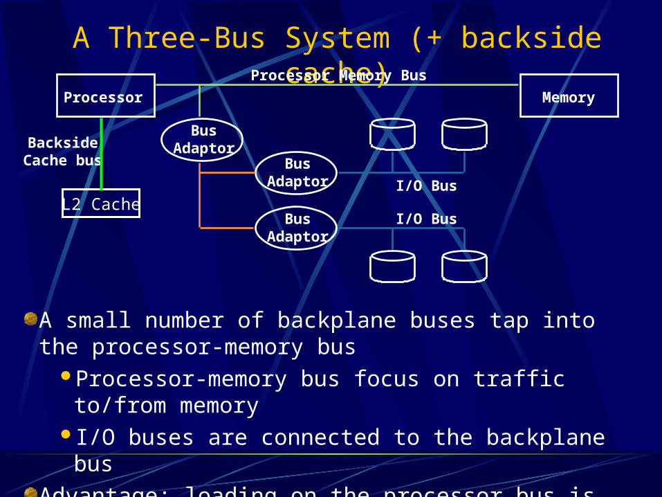
A Three-Bus System (+ backside cache)
Processor Memory
Processor Memory Bus
BusAdaptor
BusAdaptor
BusAdaptor
I/O Bus
BacksideCache bus
I/O BusL2 Cache
A small number of backplane buses tap into the processor-memory bus
Processor-memory bus focus on traffic to/from memoryI/O buses are connected to the backplane bus
Advantage: loading on the processor bus is greatly reduced & busses run at different speeds

Main components of Intel Chipset: Pentium II/III
Northbridge:Handles memoryGraphics
Southbridge: I/OPCI busDisk controllersUSB controllersAudio (AC97)Serial I/OInterrupt controllerTimers

Bunch of Wires
Physical / Mechanical Characterisics – the connectors
Electrical Specification
Timing and Signaling Specification
Transaction Protocol
What defines a bus?

Synchronous and Asynchronous Bus
Synchronous Bus:Includes a clock in the control linesA fixed protocol for communication that is relative to the
clockAdvantage: involves very little logic and can run very fastDisadvantages:
Every device on the bus must run at the same clock rate To avoid clock skew, they cannot be long if they are fast
Asynchronous Bus:It is not clockedIt can accommodate a wide range of devicesIt can be lengthened without worrying about clock skewIt requires a handshaking protocol

° ° °Master Slave
Control LinesAddress LinesData Lines
Busses so far
Bus Master: has ability to control the bus, initiates transaction
Bus Slave: module activated by the transaction
Bus Communication Protocol: specification of sequence of events and timing requirements in transferring information.
Asynchronous Bus Transfers: control lines (req, ack) serve to orchestrate sequencing.
Synchronous Bus Transfers: sequence relative to common clock.

Simplest bus paradigm
All agents operate synchronously
All can source / sink data at same rate
=> simple protocoljust manage the source and target

BReq
BG
Cmd+AddrR/WAddress
Data1 Data2Data
Simple Synchronous Protocol
Even memory busses are more complex than thismemory (slave) may take time to respondit may need to control data rate

BReq
BG
Cmd+AddrR/WAddress
Data1 Data2Data Data1
Wait
Typical Synchronous Protocol
Slave indicates when it is prepared for data xfer
Actual transfer goes at bus rate

Address
Data
Read
Req
Ack
Master Asserts Address
Master Asserts Data
Next Address
Write Transaction
t0 t1 t2 t3 t4 t5
Asynchronous Handshake
t0 : Master has obtained control and asserts address, direction, data
Waits a specified amount of time for slaves to decode target.
t1: Master asserts request line
t2: Slave asserts ack, indicating data received
t3: Master releases req
t4: Slave releases ack

Address
Data
Read
Req
Ack
Master Asserts Address Next Address
t0 t1 t2 t3 t4 t5
Read Transaction
Slave Data
t0 : Master has obtained control and asserts address, direction, data
Waits a specified amount of time for slaves to decode target.
t1: Master asserts request line
t2: Slave asserts ack, indicating ready to transmit data
t3: Master releases req, data received
t4: Slave releases ack

What is DMA (Direct Memory Access)?
Typical I/O devices must transfer large amounts of data to memory of processor:
Disk must transfer complete block (4K? 16K?)Large packets from networkRegions of video frame buffer
DMA gives external device ability to write memory directly: much lower overhead than having processor request one word at a time.
Processor (or at least memory system) acts like slave
Issue: Cache coherence:What if I/O devices write data that is currently in processor Cache?
The processor may never see new data!Solutions:
Flush cache on every I/O operation (expensive) Have hardware invalidate cache lines
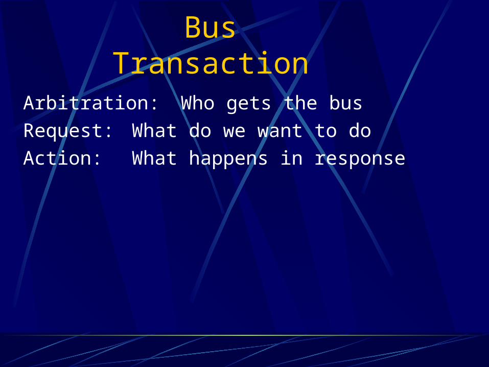
Bus Transaction
Arbitration: Who gets the bus
Request: What do we want to do
Action: What happens in response

BusMaster
BusSlave
Control: Master initiates requests
Data can go either way
Arbitration: Obtaining Access to the Bus
One of the most important issues in bus design:How is the bus reserved by a device that wishes to use it?
Chaos is avoided by a master-slave arrangement:Only the bus master can control access to the bus:
It initiates and controls all bus requestsA slave responds to read and write requests
The simplest system:Processor is the only bus masterAll bus requests must be controlled by the processorMajor drawback: the processor is involved in every
transaction

Multiple Potential Bus Masters: the Need for Arbitration
Bus arbitration scheme:A bus master wanting to use the bus asserts the bus requestA bus master cannot use the bus until its request is grantedA bus master must signal to the arbiter after finish using the bus
Bus arbitration schemes usually try to balance two factors:Bus priority: the highest priority device should be serviced firstFairness: Even the lowest priority device should never
be completely locked out from the bus
Bus arbitration schemes can be divided into four broad classes:Daisy chain arbitrationCentralized, parallel arbitrationDistributed arbitration by self-selection: each device wanting the bus
places a code indicating its identity on the bus.Distributed arbitration by collision detection:
Each device just “goes for it”. Problems found after the fact.

The Daisy Chain Bus Arbitrations Scheme
BusArbiter
Device 1HighestPriority
Device NLowestPriority
Device 2
Grant Grant Grant
Release
Request
wired-ORAdvantage: simple
Disadvantages:Cannot assure fairness: A low-priority device may be locked out indefinitely
The use of the daisy chain grant signal also limits the bus speed

BusArbiter
Device 1 Device NDevice 2
Grant Req
Centralized Parallel Arbitration
Used in essentially all processor-memory busses and in high-speed I/O busses
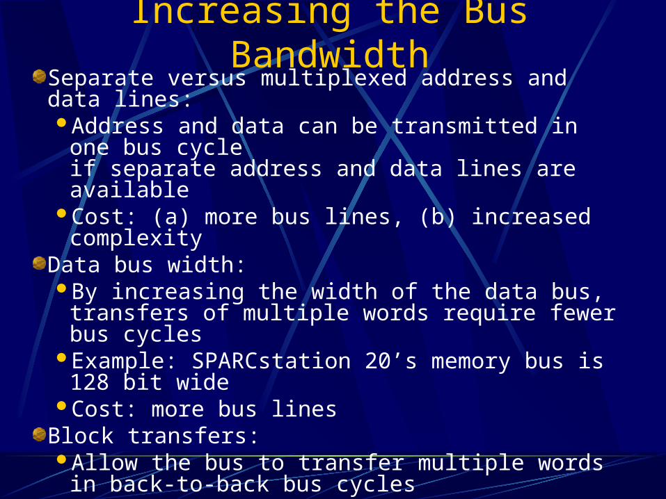
Increasing the Bus BandwidthSeparate versus multiplexed address and data lines:Address and data can be transmitted in one bus cycle
if separate address and data lines are availableCost: (a) more bus lines, (b) increased complexity
Data bus width:By increasing the width of the data bus, transfers of
multiple words require fewer bus cyclesExample: SPARCstation 20’s memory bus is 128 bit
wideCost: more bus lines
Block transfers:Allow the bus to transfer multiple words in back-to-back
bus cyclesOnly one address needs to be sent at the beginningThe bus is not released until the last word is transferredCost: (a) increased complexity
(b) decreased response time for request

Increasing Transaction Rate on Multimaster Bus
Overlapped arbitrationperform arbitration for next transaction during current
transaction
Bus parkingmaster can holds onto bus and performs multiple
transactions as long as no other master makes request
Overlapped address / data phases (prev. slide)requires one of the above techniques
Split-phase (or packet switched) buscompletely separate address and data phasesarbitrate separately for eachaddress phase yield a tag which is matched with data
phase
”All of the above” in most modern buses

PCI Read/Write TransactionsAll signals sampled on rising edge
Centralized Parallel Arbitration
overlapped with previous transaction
All transfers are (unlimited) bursts
Address phase starts by asserting FRAME#
Next cycle “initiator” asserts cmd and address
Data transfers happen on when
IRDY# asserted by master when ready to transfer data
TRDY# asserted by target when ready to transfer data
transfer when both asserted on rising edge
FRAME# deasserted when master intends to complete only one more data transfer

– Turn-around cycle on any signal driven by more than one agent
PCI Read Transaction

PCI Write Transaction

PCI OptimizationsPush bus efficiency toward 100% under common simple usage
like RISC
Bus Parkingretain bus grant for previous master until another makes
requestgranted master can start next transfer without arbitration
Arbitrary Burst lengthinitiator and target can exert flow control with xRDYtarget can disconnect request with STOP (abort or retry)master can disconnect by deasserting FRAMEarbiter can disconnect by deasserting GNT
Delayed (pended, split-phase) transactionsfree the bus after request to slow device

SummaryBuses are an important technique for building large-scale systems
Their speed is critically dependent on factors such as length, number of devices, etc.
Critically limited by capacitanceImportant terminology:
Master: The device that can initiate new transactionsSlaves: Devices that respond to the master
Two types of bus timing:Synchronous: bus includes clockAsynchronous: no clock, just REQ/ACK strobing
Direct Memory Access (dma) allows fast, burst transfer into processor’s memory:
Processor’s memory acts like a slaveProbably requires some form of cache-coherence so that DMA’ed
memory can be invalidated from cache.

The Big Picture: Where are We Now?
Control
Datapath
Memory
Processor
Input
Output
The Five Classic Components of a Computer
Next TopicLocality and Memory HierarchySRAM Memory TechnologyDRAM Memory TechnologyMemory Organization

Technology Trends
DRAM
Year Size Cycle Time
1980 64 Kb 250 ns
1983 256 Kb 220 ns
1986 1 Mb 190 ns
1989 4 Mb 165 ns
1992 16 Mb 145 ns
1995 64 Mb 120 ns
1000:1! 2:1!
Capacity Speed (latency)
Logic: 2x in 3 years 2x in 3 years
DRAM: 4x in 3 years 2x in 10 years
Disk: 4x in 3 years 2x in 10 years

µProc60%/yr.(2X/1.5yr)
DRAM9%/yr.(2X/10 yrs)1
10
100
1000
198
0198
1 198
3198
4198
5 198
6198
7198
8198
9199
0199
1 199
2199
3199
4199
5199
6199
7199
8 199
9200
0
DRAM
CPU198
2
Processor-MemoryPerformance Gap:(grows 50% / year)
Per
form
ance
Time
“Moore’s Law”
Processor-DRAM Memory Gap (latency)
Who Cares About the Memory Hierarchy?
“Less’ Law?”

Today’s Situation: Microprocessor
Rely on caches to bridge gap
Microprocessor-DRAM performance gap time of a full cache miss in instructions executed
1st Alpha (7000): 340 ns/5.0 ns = 68 clks x 2 or136 instructions
2nd Alpha (8400): 266 ns/3.3 ns = 80 clks x 4 or320 instructions
3rd Alpha (t.b.d.): 180 ns/1.7 ns =108 clks x 6 or648 instructions
1/2X latency x 3X clock rate x 3X Instr/clock 5X

Cache Performance
CPU time = (CPU execution clock cycles + Memory stall clock cycles) x clock cycle time
Memory stall clock cycles = (Reads x Read miss rate x Read miss penalty + Writes x Write miss rate x Write miss penalty)
Memory stall clock cycles = Memory accesses x Miss rate x Miss penalty

Impact on PerformanceSuppose a processor executes at
Clock Rate = 200 MHz (5 ns per cycle)Base CPI = 1.1 50% arith/logic, 30% ld/st, 20% control
Suppose that 10% of memory operations get 50 cycle miss penaltySuppose that 1% of instructions get same miss penaltyCPI = Base CPI + average stalls per instruction
1.1(cycles/ins) +[ 0.30 (DataMops/ins)
x 0.10 (miss/DataMop) x 50 (cycle/miss)] +[ 1 (InstMop/ins)
x 0.01 (miss/InstMop) x 50 (cycle/miss)] = (1.1 + 1.5 + .5) cycle/ins = 3.1
55% of the time the proc is stalled waiting for memory!
Ideal CPI 1.1Data Miss 1.5Inst Miss 0.5

The Goal: illusion of large, fast, cheap memory
Fact: Large memories are slow, fast memories are small
How do we create a memory that is large, cheap and fast (most of the time)?
HierarchyParallelism

Why hierarchy works
Address Space0 2^n - 1
Probabilityof reference
The Principle of Locality:Program access a relatively small portion of the address space at any instant of time.

Memory Hierarchy: How Does it Work?
Lower LevelMemoryUpper Level
MemoryTo Processor
From ProcessorBlk X
Blk Y
Temporal Locality (Locality in Time):=> Keep most recently accessed data items closer to the processor
Spatial Locality (Locality in Space):=> Move blocks consists of contiguous words to the upper levels

Memory Hierarchy: Terminology
Lower LevelMemoryUpper Level
MemoryTo Processor
From ProcessorBlk X
Blk Y
Hit: data appears in some block in the upper level of the hierarchy (example: Block X is found in the L1 cache)
Hit Rate: the fraction of memory access found in the upper levelHit Time: Time to access the upper level which consists of
RAM access time + Time to determine hit/miss
Miss: data needs to be retrieve from a block in the lower level in the hierachy (Block Y is not in L1 cache and must be fetched from main memory)
Miss Rate = 1 - (Hit Rate)Miss Penalty: Time to replace a block in the upper level +
Time to deliver the block the processor
Hit Time << Miss Penalty
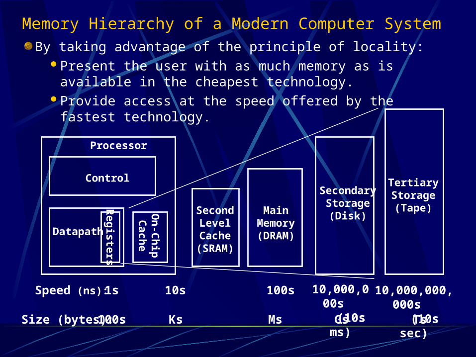
Memory Hierarchy of a Modern Computer System
Control
Datapath
SecondaryStorage(Disk)
Processor
Registers
MainMemory(DRAM)
SecondLevelCache
(SRAM)
On
-Ch
ipC
ache
1s 10,000,000s
(10s ms)
Speed (ns): 10s 100s
100s GsSize (bytes): Ks Ms
TertiaryStorage(Tape)
10,000,000,000s (10s sec)
Ts
By taking advantage of the principle of locality:Present the user with as much memory as is available in the
cheapest technology.Provide access at the speed offered by the fastest technology.
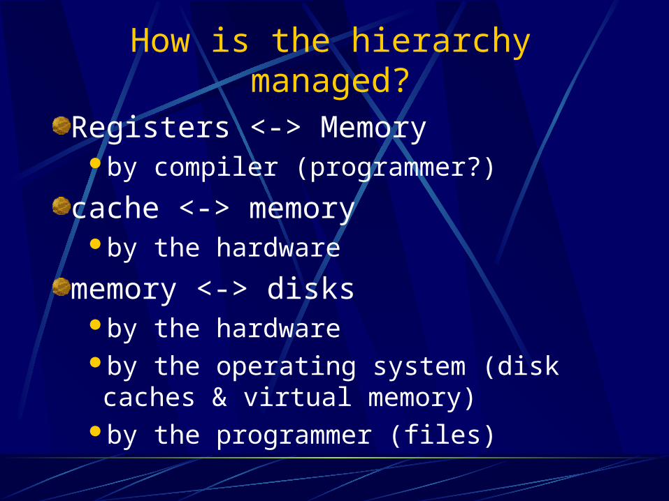
How is the hierarchy managed?
Registers <-> Memoryby compiler (programmer?)
cache <-> memoryby the hardware
memory <-> disksby the hardwareby the operating system (disk caches & virtual memory)
by the programmer (files)

Memory Hierarchy TechnologyRandom Access:“Random” is good: access time is the same for all locationsDRAM: Dynamic Random Access Memory
High density, low power, cheap, slow Dynamic: need to be “refreshed” regularly (1-2% of cycles)
SRAM: Static Random Access Memory Low density, high power, expensive, fast Static: content will last “forever”(until lose power)
“Non-so-random” Access Technology:Access time varies from location to location and from time to timeExamples: Disk, CDROM
Sequential Access Technology: access time linear in location (e.g.,Tape)
We will concentrate on random access technologyThe Main Memory: DRAMs + Caches: SRAMs

Main Memory BackgroundPerformance of Main Memory:
Latency: Cache Miss Penalty Access Time: time between request and word arrives Cycle Time: time between requests
Bandwidth: I/O & Large Block Miss Penalty (L2)
Main Memory is DRAM : Dynamic Random Access MemoryDynamic since needs to be refreshed periodically (8 ms)Addresses divided into 2 halves (Memory as a 2D matrix):
RAS or Row Access Strobe CAS or Column Access Strobe
Cache uses SRAM : Static Random Access MemoryNo refresh (6 transistors/bit vs. 1 transistor)
Size: DRAM/SRAM 4-8 Cost/Cycle time: SRAM/DRAM 8-16

Random Access Memory (RAM) Technology
Why do computer designers need to know about RAM technology?
Processor performance is usually limited by memory bandwidth
As IC densities increase, lots of memory will fit on processor chip
Tailor on-chip memory to specific needs- Instruction cache- Data cache- Write buffer
What makes RAM different from a bunch of flip-flops?Density: RAM is much denser

Main Memory Deep Background
“Out-of-Core”, “In-Core,” “Core Dump”?
“Core memory”?
Non-volatile, magnetic
Lost to 4 Kbit DRAM (today using 64Mbit DRAM)
Access time 750 ns, cycle time 1500-3000 ns

Write:
1. Drive bit lines (bit=1, bit=0)
2. Select row
Read:
1. Precharge bit and bit to Vdd or Vdd/2 => make sure equal!
2.. Select row
3. Cell pulls one line low
4. Sense amp on column detects difference between bit and bit
Static RAM Cell6-Transistor SRAM Cell
bit bit
word(row select)
bit bit
word
replaced with pullupto save area
10
0 1

Typical SRAM Organization: 16-word x 4-bit
SRAMCell
SRAMCell
SRAMCell
SRAMCell
SRAMCell
SRAMCell
SRAMCell
SRAMCell
SRAMCell
SRAMCell
SRAMCell
SRAMCell
- +Sense Amp - +Sense Amp - +Sense Amp - +Sense Amp
: : : :
Word 0
Word 1
Word 15
Dout 0Dout 1Dout 2Dout 3
- +Wr Driver &Precharger - +
Wr Driver &Precharger - +
Wr Driver &Precharger - +
Wr Driver &Precharger
Ad
dress D
ecoder
WrEnPrecharge
Din 0Din 1Din 2Din 3
A0
A1
A2
A3

A
DOE_L
2 Nwordsx M bitSRAM
N
M
WE_L
Logic Diagram of a Typical SRAM
Write Enable is usually active low (WE_L)
Din and Dout are combined to save pins:A new control signal, output enable (OE_L) is neededWE_L is asserted (Low), OE_L is disasserted (High)
D serves as the data input pinWE_L is disasserted (High), OE_L is asserted (Low)
D is the data output pinBoth WE_L and OE_L are asserted:
Result is unknown. Don’t do that!!!

Typical SRAM Timing
Write Timing:
D
Read Timing:
WE_L
A
WriteHold Time
Write Setup Time
A
DOE_L
2 Nwordsx M bitSRAM
N
M
WE_L
Data In
Write Address
OE_L
High Z
Read Address
Junk
Read AccessTime
Data Out
Read AccessTime
Data Out
Read Address

1-Transistor Memory Cell (DRAM)
row select
bit
Write:1. Drive bit line2.. Select row
Read:1. Precharge bit line to Vdd2.. Select row3. Cell and bit line share charges
Very small voltage changes on the bit line4. Sense (fancy sense amp)
Can detect changes of ~1 million electrons5. Write: restore the value
Refresh1. Just do a dummy read to every cell.

Classical DRAM Organization (square)
row
decoder
rowaddress
Column Selector & I/O Circuits Column
Address
data
RAM Cell Array
word (row) select
bit (data) lines
Each intersection representsa 1-T DRAM Cell
Row and Column Address together: Select 1 bit a time
AD
OE_L
256K x 8DRAM9 8
WE_LCAS_LRAS_L
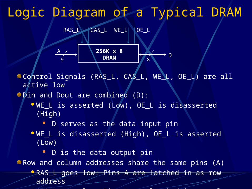
Logic Diagram of a Typical DRAM
Control Signals (RAS_L, CAS_L, WE_L, OE_L) are all active low
Din and Dout are combined (D):WE_L is asserted (Low), OE_L is disasserted (High)
D serves as the data input pinWE_L is disasserted (High), OE_L is asserted (Low)
D is the data output pin
Row and column addresses share the same pins (A)RAS_L goes low: Pins A are latched in as row addressCAS_L goes low: Pins A are latched in as column addressRAS/CAS edge-sensitive

AD
OE_L
256K x 8DRAM9 8
WE_LCAS_LRAS_L
OE_L
A Row Address
WE_L
Junk
Read AccessTime
Output EnableDelay
CAS_L
RAS_L
Col Address Row Address JunkCol Address
D High Z Data Out
DRAM Read Cycle Time
Early Read Cycle: OE_L asserted before CAS_L Late Read Cycle: OE_L asserted after CAS_L
Junk Data Out High Z
DRAM Read TimingEvery DRAM access begins at:
The assertion of the RAS_L2 ways to read:
early or late v. CAS

AD
OE_L
256K x 8DRAM9 8
WE_LCAS_LRAS_L
WE_L
A Row Address
OE_L
Junk
WR Access Time WR Access Time
CAS_L
RAS_L
Col Address Row Address JunkCol Address
D Junk JunkData In Data In Junk
DRAM WR Cycle Time
Early Wr Cycle: WE_L asserted before CAS_L Late Wr Cycle: WE_L asserted after CAS_L
DRAM Write TimingEvery DRAM access begins at:
The assertion of the RAS_L2 ways to write:
early or late v. CAS

Key DRAM Timing Parameters
tRAC: minimum time from RAS line falling to the valid data output.
Quoted as the speed of a DRAM A fast 4Mb DRAM tRAC = 60 ns
tRC: minimum time from the start of one row access to the start of the next.
tRC = 110 ns for a 4Mbit DRAM with a tRAC of 60 ns
tCAC: minimum time from CAS line falling to valid data output.
15 ns for a 4Mbit DRAM with a tRAC of 60 ns
tPC: minimum time from the start of one column access to the start of the next.
35 ns for a 4Mbit DRAM with a tRAC of 60 ns

DRAM PerformanceA 60 ns (tRAC) DRAM can
perform a row access only every 110 ns (tRC)
perform column access (tCAC) in 15 ns, but time between column accesses is at least 35 ns (tPC).
In practice, external address delays and turning around buses make it 40 to 50 ns
These times do not include the time to drive the addresses off the microprocessor nor the memory controller overhead.
Drive parallel DRAMs, external memory controller, bus to turn around, SIMM module, pins…
180 ns to 250 ns latency from processor to memory is good for a “60 ns” (tRAC) DRAM

Interleaved: CPU, Cache, Bus 1 word:
Memory N Modules(4 Modules); example is word interleaved
Wide: CPU/Mux 1 word;
Mux/Cache, Bus, Memory N words (Alpha: 64 bits & 256 bits)
Main Memory Performance
Simple: CPU, Cache, Bus,
Memory same width (32 bits)

TimeAccess Time
Cycle Time
Main Memory Performance
DRAM (Read/Write) Cycle Time >> DRAM (Read/Write) Access Time
2:1; why?
DRAM (Read/Write) Cycle Time :How frequent can you initiate an access?Analogy: A little kid can only ask his father for money on Saturday
DRAM (Read/Write) Access Time:How quickly will you get what you want once you initiate an
access?Analogy: As soon as he asks, his father will give him the money
DRAM Bandwidth Limitation analogy:What happens if he runs out of money on Wednesday?

Access Pattern without Interleaving:
Start Access for D1
CPU Memory
Start Access for D2
D1 available
Access Pattern with 4-way Interleaving:
Acc
ess
Ban
k 0
Access Bank 1
Access Bank 2
Access Bank 3
We can Access Bank 0 again
CPU
MemoryBank 1
MemoryBank 0
MemoryBank 3
MemoryBank 2
Increasing Bandwidth - Interleaving

address
Bank 0
048
12
address
Bank 1
159
13
address
Bank 2
26
1014
address
Bank 3
37
1115
Main Memory PerformanceTiming model
1 to send address, 4 for access time, 10 cycle time, 1 to send
dataCache Block is 4 words
Simple M.P. = 4 x (1+10+1) = 48Wide M.P. = 1 + 10 + 1 = 12Interleaved M.P. = 1+10+1 + 3 =15

Independent Memory Banks
How many banks?number banks number clocks to access word in bank
For sequential accesses, otherwise will return to original bank before it has next word ready
Increasing DRAM => fewer chips => harder to have banks
Growth bits/chip DRAM : 50%-60%/yrNathan Myrvold M/S: mature software growth (33%/yr for NT) growth MB/$ of DRAM (25%-30%/yr)

Fewer DRAMs/System over TimeM
inim
um
PC
Mem
ory
Siz
e
DRAM Generation‘86 ‘89 ‘92 ‘96 ‘99 ‘02 1 Mb 4 Mb 16 Mb 64 Mb 256 Mb 1 Gb
4 MB
8 MB
16 MB
32 MB
64 MB
128 MB
256 MB
32 8
16 4
8 2
4 1
8 2
4 1
8 2
Memory per System growth@ 25%-30% / year
Memory per DRAM growth@ 60% / year
(from PeteMacWilliams, Intel)

Fast Page Mode Operation
N r
ows
N cols
DRAM
ColumnAddress
M-bit OutputM bits
N x M “SRAM”
RowAddress
A Row Address
CAS_L
RAS_L
Col Address Col Address
1st M-bit Access
Col Address Col Address
2nd M-bit 3rd M-bit 4th M-bit
Regular DRAM Organization:N rows x N column x M-bitRead & Write M-bit at a timeEach M-bit access requires
a RAS / CAS cycleFast Page Mode DRAM
N x M “SRAM” to save a rowAfter a row is read into the register
Only CAS is needed to access other M-bit blocks on that row
RAS_L remains asserted while CAS_L is toggled
FP Mode DRAM
Fast page mode DRAMIn page mode, a row of the DRAM can be kept "open", so
that successive reads or writes within the row do not suffer the delay of precharge and accessing the row. This increases the performance of the system when reading or writing bursts of data.

Key DRAM Timing ParameterstRAC: minimum time from RAS line falling to the valid data output.
Quoted as the speed of a DRAM A fast 4Mb DRAM tRAC = 60 ns
tRC: minimum time from the start of one row access to the start of the next.
tRC = 110 ns for a 4Mbit DRAM with a tRAC of 60 ns
tCAC: minimum time from CAS line falling to valid data output.
15 ns for a 4Mbit DRAM with a tRAC of 60 ns
tPC: minimum time from the start of one column access to the start of the next.
35 ns for a 4Mbit DRAM with a tRAC of 60 ns
SDRAM: Syncronous DRAM?
More complicated, on-chip controllerOperations syncronized to clockSo, give row address one cycle
Column address some number of cycles later (say 3) Date comes out later (say 2 cycles later)
Burst modes Typical might be 1,2,4,8, or 256 length burst Thus, only give RAS and CAS once for all of these accesses
Multi-bank operation (on-chip interleaving) Lets you overlap startup latency (5 cycles above) of two banks
Careful of timing specs!10ns SDRAM may still require 50ns to get first data! 50ns DRAM means first data out in 50ns

Other Types of DRAM
Extended data out (EDO) DRAM similar to Fast Page Mode DRAMadditional feature that a new access cycle can be started
while keeping the data output of the previous cycle active. This allows a certain amount of overlap in operation (pipelining), allowing somewhat improved speed. It was 5% faster than Fast Page Mode DRAM, which it began to replace in 1993.
Other Types of DRAM
Double data rate (DDR) SDRAMDouble data rate (DDR) SDRAM is a later development of
SDRAM, used in PC memory from 2000 onwards. All types of SDRAM use a clock signal that is a square wave.
This means that the clock alternates regularly between one voltage (low) and another (high), usually millions of times per second. Plain SDRAM, like most synchronous logic circuits, acts on the low-to-high transition of the clock and ignores the opposite transition. DDR SDRAM acts on both transitions, thereby halving the required clock rate for a given data transfer rate.

Memory Systems: Delay more than RAW DRAM
DRAM2^n x 1chip
DRAMController
address
MemoryTimingController Bus Drivers
n
w
Tc = Tcycle + Tcontroller + Tdriver

DRAMs over TimeDRAM Generation
‘84 ‘87 ‘90 ‘93 ‘96 ‘99
1 Mb 4 Mb 16 Mb 64 Mb 256 Mb 1 Gb
55 85 130 200 300 450
30 47 72 110 165 250
28.84 11.1 4.26 1.64 0.61 0.23
(from Kazuhiro Sakashita, Mitsubishi)
1st Gen. Sample
Memory Size
Die Size (mm2)
Memory Area (mm2)
Memory Cell Area (µm2)

SummaryTwo Different Types of Locality:
Temporal Locality (Locality in Time): If an item is referenced, it will tend to be referenced again soon.
Spatial Locality (Locality in Space): If an item is referenced, items whose addresses are close by tend to be referenced soon.
By taking advantage of the principle of locality:Present the user with as much memory as is available in the
cheapest technology.Provide access at the speed offered by the fastest technology.
DRAM is slow but cheap and dense:Good choice for presenting the user with a BIG memory system
SRAM is fast but expensive and not very dense:Good choice for providing the user FAST access time.


