Optimization and implementation of a multi-level buck converter for standard CMOS on-chip integration International Workshop on Power Supply On Chip September 22nd - 24th, 2008, Cork, Ireland Vahid Yousefzadeh, Toru Takayama Dragan Maksimović Colorado Power Electronics Center ECE Department, 425 UCB University of Colorado Boulder, CO 80309-0425 [email protected]Gerard Villar Eduard Alarcón Dept. of Electronic Engineering Technical University of Catalunya Campus Nord UPC – Building C4 08034 Barcelona, Spain [email protected]
Transcript
Optimization and implementation of a multi-level buck converter for standard CMOS on-chip integration
International Workshop on Power Supply On ChipSeptember 22nd - 24th, 2008, Cork, Ireland
Vahid Yousefzadeh, Toru Takayama
Dragan Maksimović
Colorado Power Electronics CenterECE Department, 425 UCB
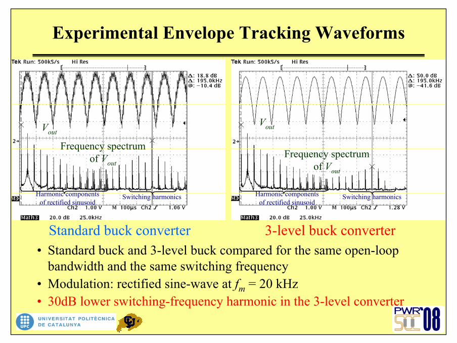
Standard buck converter• Standard buck and 3-level buck compared for the same open-loop
bandwidth and the same switching frequency• Modulation: rectified sine-wave at fm = 20 kHz• 30dB lower switching-frequency harmonic in the 3-level converter
3-level buck converter
Cx+
-VC
Vin
g1
g2
g3g4
VSW
+_y
+_
Vin/2 - Vq/2
Vin/2 + Vq/2
VSW
x
g3=d(t)+ dg1=d(t)
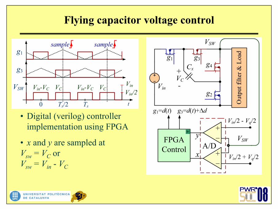
Flying capacitor voltage control
• Digital (verilog) controller implementation using FPGA
• x and y are sampled atVsw = VC orVsw = Vin - VC
VSWVin
Vin/2Vin-VC Vin-VCVC VC
g1
g3
TsTs/20 t
sample sample
Experimental waveforms for flying capacitor voltage control
Vsw
g1
g3
Vsw
g1
g3
Uncontrolled capacitor Cx
voltage
Controlled capacitor Cx
voltage
Vin-Vc Vc
D > 0.5
Vin-Vc Vc
D > 0.5
VcVin-Vc
D < 0.5
Vin-Vc Vc
D < 0.5
• Introduction and motivation• Series-connected multiphase multilevel buck converter
• Design-space optimization• Mixed-signal implementation in 0.25µm TSMC CMOS
– Air-core bondingwire-based inductor, tapered buffer and transistor design– Inductor current zero-crossing detection circuit
• Conclusions
Outline
Low-Cx resonant 3-level buck converter in DCM. Self-driving transistor-level topology
Self-driving scheme to interconnect power transistors and drivers, which reduces the voltage across the power MOSFETs gate dielectric.
3-level self-driving PFM low-Cx buck converter
Driver supply voltage and vgs for all power MOSFETs, Cadence transistor-level simulations.
37 MHz switching frequency26 nH inductance
3-level self-driving PFM low-Cx buck converter
• Use of core transistors to implement the power MOSFETs• Use of core transistors to implement power drivers of P2 & N2• Reduces the power consumption of the power drivers
Representative waveforms corresponding to a DCM operated 3-level Buck converter, duty cycle below 50%
Control signal-to-output voltage transfer function comparison between the 3-level (Cxsweep) and the classical (dotted line) Buck converters.
Output voltage ripple as a function of Vo, for the 3-level (Cx sweep) and the classical (dotted line) Buck converters.
3-level self-driving PFM low-Cx buck converter
L=35nHCo=30nFfs=25MHz
Vbat=3.6VVo=1VIo=100mA
• Introduction and motivation• Series-connected multiphase multilevel buck converter
• Design-space optimization• Mixed-signal implementation in 0.25µm TSMC CMOS
– Air-core bondingwire-based inductor, tapered buffer and transistor design– Inductor current zero-crossing detection circuit
• Conclusions
Outline
•Area underneath inductor is usable for capacitors and power MOSFETs
Bondwire triangular spiral inductors in standard CMOS
Complete loss optimization of on-chip CMOS synchronous rectifier
Power MOSFETs
Breakdown of loss distribution, corresponding the optimized design of power MOSFETs and their associated drivers.
WP = 3092µm WN = 2913µm powerdrivers with 7.59 and 7.48 tapering factorsOverall losses 37.1mW
Additional degree of freedom: impact of Wp upon efficiency and delay
Power MOSFET gate drive design
Qi and Qe1 variation as a function of the PMOS channel width of the minimum inverter (Wn = 0.3µm)
tfri and tfre1 parameter variation
Total energy losses as a function of the number of inverters n and the minimum inverter PMOS channel width Wp. The area includes all the designs constrainted to a propagation delay lower than 1.15 ns.
iL>0 iL<0
7.7
The body diode of the NMOS power switch turns-on as a consequence of a premature cut
off of the power transistor
iL=0 detection circuit. Event detection
Inductor current charges the x-node parasitic capacitor and a positive voltage pulse appears in Vx
voltage, due to late cut off of the power transistor
iL=0 detection circuit. Circuit for time adjustment. Inductor current observer
iL>0
iL<0
N1
N2
7.9
iL=0 detection circuit Mixed-signal implementation in 0.25µm CMOS
Before adjustment After iL=0 adjustment
7.10
Time-domain performance of iL=0 detection circuit
2370 µm
P1
2630 µm
P2
N1N2 7.17
Complete integrated 3-level CMOS switching power converter
7.19
Full-transistor-level circuit results (I)
7.20
Full-transistor-level circuit results (II)
7.21
Full-transistor-level circuit results (III)
Experimental results
• Introduction and motivation• Series-connected multiphase multilevel buck converter
• Design-space optimization• Mixed-signal implementation in 0.25µm TSMC CMOS
– Air-core bondingwire-based inductor, tapered buffer and transistor design– Inductor current zero-crossing detection circuit
• Conclusions
Outline
• Three-level converter results in favorable trade-offs in terms of decreasing the switching ripples, decreasing the switching frequency, reducing the size of the filter elements, increasing the converter open-loop bandwidth, or increasing the converter efficiency.
• The 3-level converter with low-Cx, self-biased drivers and operating in DCM/PFM has been presented as a candidate for DC-DC converter integration
• The use of the self-driving scheme to supply the drivers allows the use of thin-oxide transistors which increases the performance of the switches.
• Design optimization results in the 3-level converter outperforming the Buck converter.
Future research lines• Linear-assisted scheme for multilevel converters• Explore extending the approach to more intermediate levels• Use different modulations (e.g. asynchronous sigma delta)• Applying time optimal control