Organic Electronic Devices Week 5: Organic Light-Emitting Devices and Emerging Technologies Lecture 5.5: Course Review and Summary Bryan W. Boudouris Chemical Engineering Purdue University 1
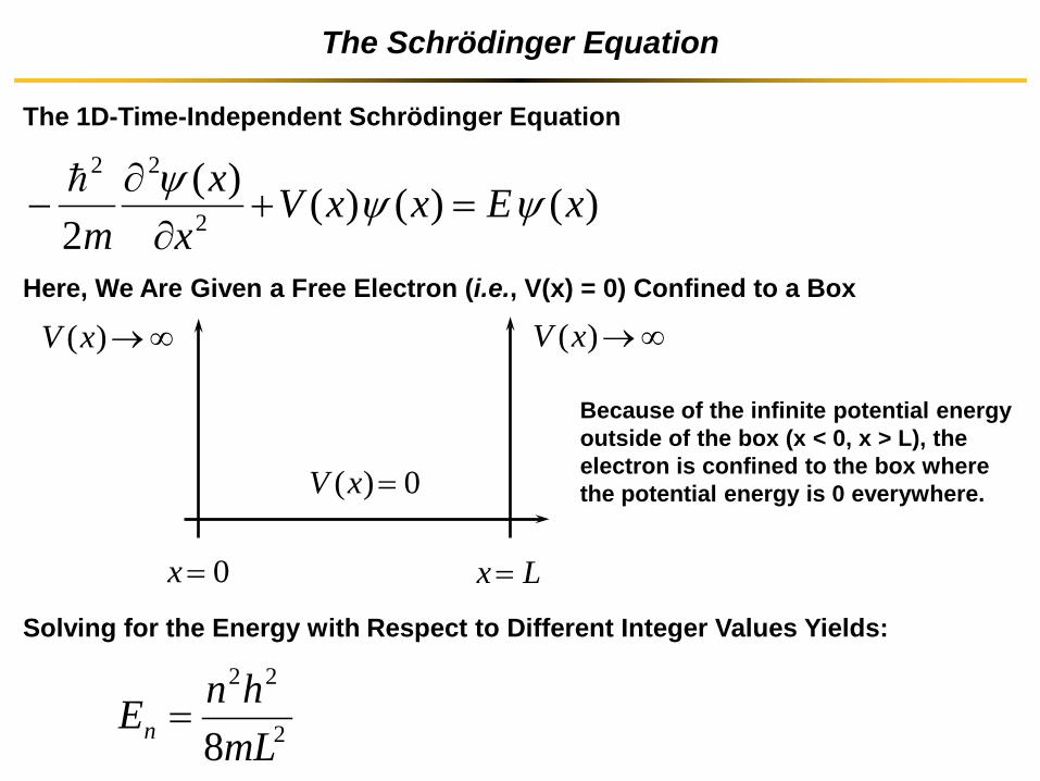
Solving for the Energy with Respect to Different Integer Values Yields:
2
22
8mLhnEn =
Here, We Are Given a Free Electron (i.e., V(x) = 0) Confined to a Box
0)( =xV
∞→)(xV∞→)(xV
0=x Lx =
Because of the infinite potential energy outside of the box (x < 0, x > L), the electron is confined to the box where the potential energy is 0 everywhere.
The Fermi-Dirac Distribution is a Function of Temperature
At Temperatures Above 0 K There is a Non-Zero Probability Associated with f(E)
Plots of D(E), f(E), n, and p as a Function of Energy
D(E) f(E) n(E), p(E)
Density of States Fermi-Dirac Distribution
Electron and Hole Densities
Image Reproduced From: The Dissertation of Robert Wittmann. http://www.iue.tuwien.ac.at/phd/wittmann/diss.html.
Imagine a Polymer Chain with Three Chromophoric Units
An extra electron is added to the first chromophoric unit such that the electron density on the black portion of the polymer chain is higher than that of the blue and the red segments. The non-equilibrium electron distribution, causes the first segment to pass the extra charge to the second segment. Then, the second segment may pass the electron density to the third segment, or the charge may be passed back to the first segment.
Now, we need to develop a mathematical model that will allow us to describe the rate of charge transport using this type of system.
The black, blue, and red segments of the polymer chain are all one molecule. However, some chemical or structural defect causes them to have a break in conjugation between the segments. Within each chromophoric unit, however, there is going to be electronic coupling, so we can think of the electron as being delocalized across a single chromophoric unit in the polymer chain.
Doping Introduces New Energy Levels in Semiconductors
Imagine a Traditional Inorganic Semiconductor, Silicon
Si Si Si Si Si
Si Si Si Si
Si
Intrinsic Si
Intrinsic Si Band Diagram
EV
EC
Band Gap Energy (Eg) Eg = 1.1 eV
Ei
n-Doped Extrinsic Si
Si Si Si Si
Si Si Si Si
Si P Si Si Si
Si Si Si Si
Si
P Has 5 Valence Atoms
Doped Si Band Diagram
EV
EC
Band Gap Energy (Eg) Eg = 1.1 eV
ED
Ec – ED << Eg
Introduction to the Multiple Trap and Thermal Release (MTR) Model
Imagine a Transport Band with Impurity States
The key difference between band transport in traditional solid state physics and organic electronic devices is the LARGE AMOUNT OF DISORDER in most organic electronic systems relative to inorganic semiconductors. In some organic materials, transport is limited by localized states induced by defects and unwanted impurities. These defects and impurities are referred to by the catchall term of traps.
Energy
EC
ET,1
ET,2
ET,3
Localized states with trap energies at 3 distinct energy levels
There is a finite probability that the carrier will be trapped in (and that the carrier will be released from) one of the lower energy trap states available due to the defects and impurities.
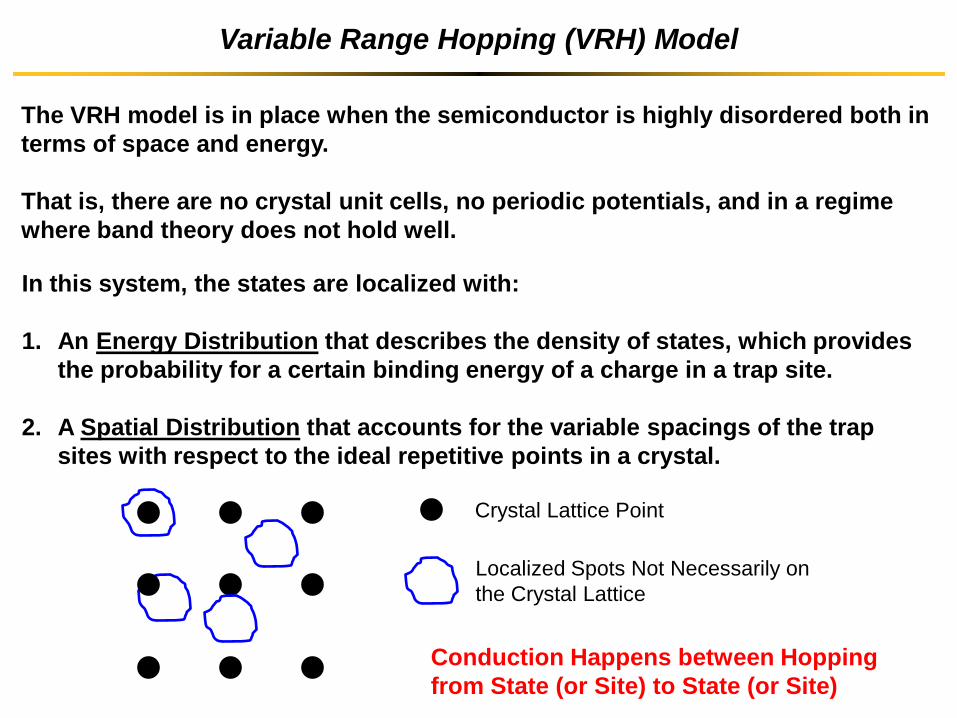
Variable Range Hopping (VRH) Model
The VRH model is in place when the semiconductor is highly disordered both in terms of space and energy. That is, there are no crystal unit cells, no periodic potentials, and in a regime where band theory does not hold well.
In this system, the states are localized with: 1. An Energy Distribution that describes the density of states, which provides
the probability for a certain binding energy of a charge in a trap site.
2. A Spatial Distribution that accounts for the variable spacings of the trap sites with respect to the ideal repetitive points in a crystal.
Crystal Lattice Point
Localized Spots Not Necessarily on the Crystal Lattice
Conduction Happens between Hopping from State (or Site) to State (or Site)
OFET Device Structure and Operating Mechanism
Organic Field-effect Transistors (OFETs) Are Useful Devices for Testing the Properties of Organic Semiconductors
OFETs Are Three Electrode Devices
S – Source Electrode D – Drain Electrode Gate – Gate Electrode VG – Voltage Between Source and Gate VD – Voltage Between Source and Drain L – Channel Length, Distance between Source and Drain Electrodes (Typical Value ~200 µm) W – Channel Width, Distance of the Source and Drain Electrodes in the Direction Orthogonal to the Channel Length Direction (Typical Value ~2,000 µm)
Operating Mechanism of an OFET in Hole Transporting Mode
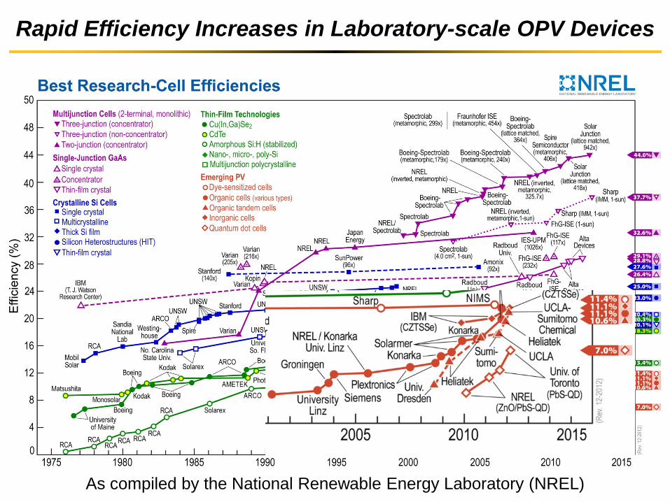
Rapid Efficiency Increases in Laboratory-scale OPV Devices
As compiled by the National Renewable Energy Laboratory (NREL)
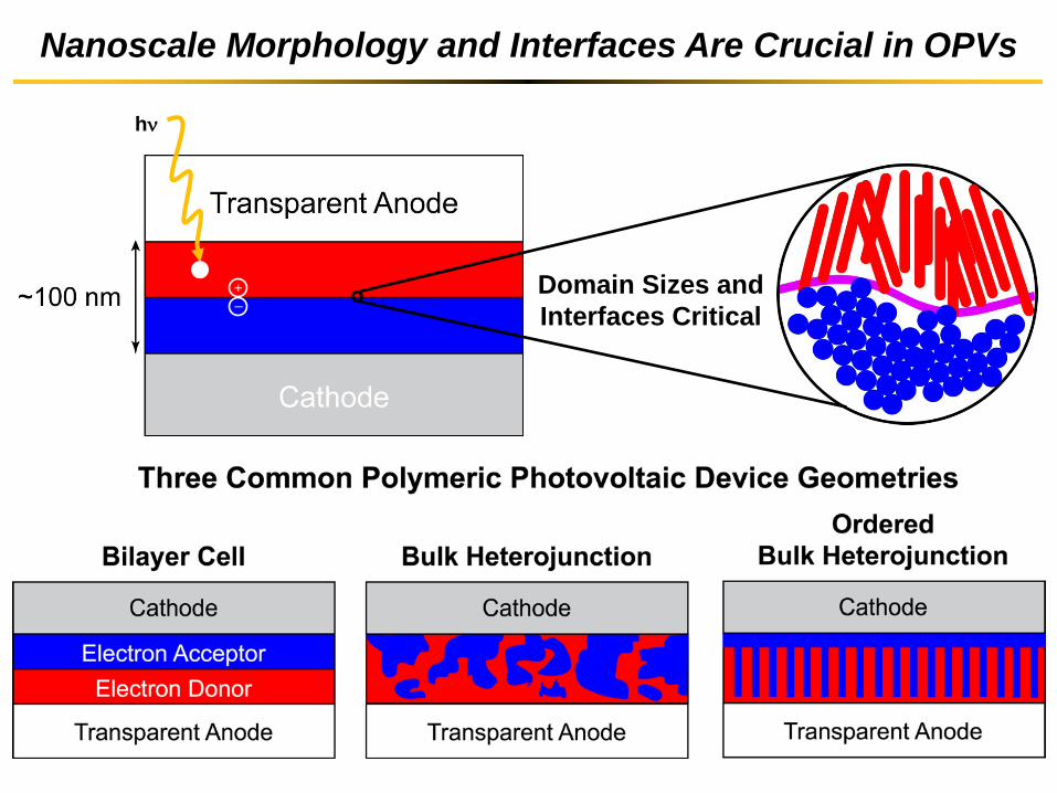
Domain Sizes and Interfaces Critical
+ –
hν
Nanoscale Morphology and Interfaces Are Crucial in OPVs
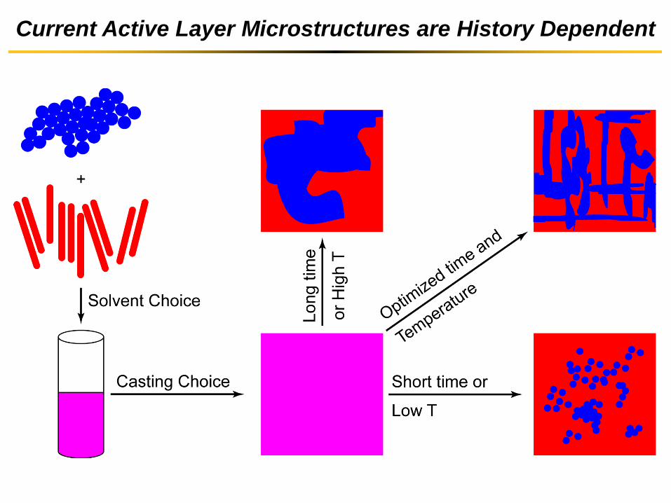
Current Active Layer Microstructures are History Dependent
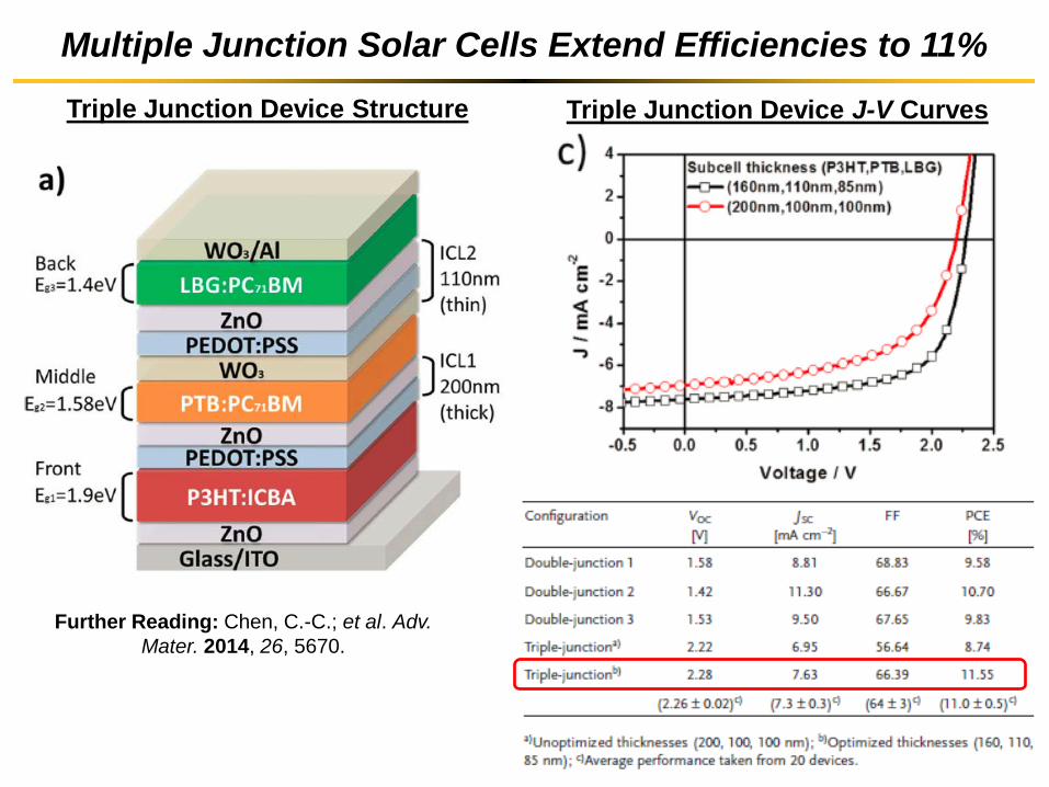
Multiple Junction Solar Cells Extend Efficiencies to 11%
Further Reading: Chen, C.-C.; et al. Adv. Mater. 2014, 26, 5670.