1 rev. 1.2, 2016-Nov-23 Feature Highlights • Powerful switch module for any type of DC loads • Replaces Relays and SSRs • Two channels • High-power MOSFETs with very low Rds(On) of just 1.4mΩ • Opto-isolated power and control circuits • Up to 55A per board without fan • Control voltage: 3.3-16V, logic-level compatible • Load voltage: 12-24V • Protection diodes for driving inductive loads • Channels can be combined together to deliver the maximum power to heavy load • “Channel-ON” and “Power-ON” LEDs • Tiny size: just 50х68 mm • 2 additional power connectors • Open-Source and Open-Hardware • Developed and made in Russia 1 Overview Cheap3D MOSFET Switch Board is a tiny yet very powerful module designed to drive high-current DC loads such as 3D printer heated beds, extruder heaters, LED lighting stripes, motors, etc. There are two power channels, which can be controlled independently or can be combined to drive one much higher load. The board is intended to replace weak MOSFETs found on cheaper RepRap boards such as RAMPS, RAMBO, RUMBA, MKS Gen, etc. It is also an ideal solution for driving high-power loads instead of regular Relays, or Solid-State Relays (SSRs) which build up a lot of heat and frequently require massive heatsinks. Both channels are opto-isolated so no current flows between input (“Logic”) side and output (“Power”) side, which allows usage of different PSUs for control board and the load. MOSFETs used have extremely low Rds(ON) resistance of just 1.4mΩ (reduced to overall 0.7mΩ with channels combined) so the voltage drop on board is lowest possible (much lower than SSRs), and for most loads this board requires no fan or heatsink at all. Powerside has built-in reverse protection diodes which protect MOSFETs from voltage spikes when used with inductive loads. The control side is fully compatible with virtually any MCU board (Arduino included) that can supply 3.3V (up to 16V) logic level signals. Low-frequency PWM operation is also supported. The board utilizes two convenient standard 2.54mm pitch output power connectors that can be used to drive fans, backlight, etc up to 500mA per each connector. Fig. 1. Board top view
Transcript
1 rev. 1.2, 2016-Nov-23
Feature Highlights
• Powerful switch module for any type of DC loads • Replaces Relays and SSRs • Two channels • High-power MOSFETs with very low Rds(On) of just 1.4mΩ • Opto-isolated power and control circuits • Up to 55A per board without fan • Control voltage: 3.3-16V, logic-level compatible • Load voltage: 12-24V • Protection diodes for driving inductive loads • Channels can be combined together to deliver the maximum
power to heavy load • “Channel-ON” and “Power-ON” LEDs • Tiny size: just 50х68 mm • 2 additional power connectors • Open-Source and Open-Hardware • Developed and made in Russia
1 Overview
Cheap3D MOSFET Switch Board is a tiny yet very powerful module designed to drive high-current DC loads such as 3D printer heated beds, extruder heaters, LED lighting stripes, motors, etc. There are two power channels, which can be controlled independently or can be combined to drive one much higher load.
The board is intended to replace weak MOSFETs found on cheaper RepRap boards such as RAMPS, RAMBO, RUMBA, MKS Gen, etc. It is also an ideal solution for driving high-power loads instead of regular Relays, or Solid-State Relays (SSRs) which build up a lot of heat and frequently require massive heatsinks.
Both channels are opto-isolated so no current flows between input (“Logic”) side and output (“Power”) side, which allows usage of different PSUs for control board and the load.
MOSFETs used have extremely low Rds(ON) resistance of just 1.4mΩ (reduced to overall 0.7mΩ with channels combined) so the voltage drop on board is lowest possible (much lower than SSRs), and for most loads this board requires no fan or heatsink at all.
Powerside has built-in reverse protection diodes which protect MOSFETs from voltage spikes when used with inductive loads.
The control side is fully compatible with virtually any MCU board (Arduino included) that can supply 3.3V (up to 16V) logic level signals. Low-frequency PWM operation is also supported.
The board utilizes two convenient standard 2.54mm pitch output power connectors that can be used to drive fans, backlight, etc up to 500mA per each connector.
Fig. 1. Board top view
2 rev. 1.2, 2016-Nov-23
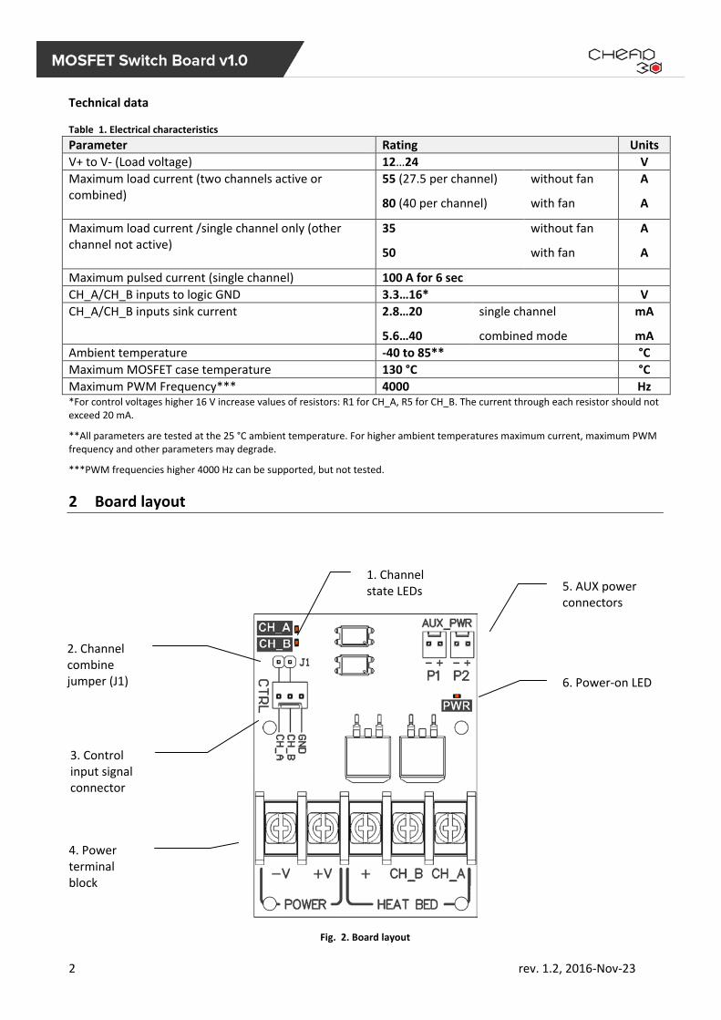
Technical data
Table 1. Electrical characteristics Parameter Rating Units V+ to V- (Load voltage) 12…24 V Maximum load current (two channels active or combined)
55 (27.5 per channel)
80 (40 per channel)
without fan
with fan
A
A
Maximum load current /single channel only (other channel not active)
35
50
without fan
with fan
A
A
Maximum pulsed current (single channel) 100 A for 6 sec CH_A/CH_B inputs to logic GND 3.3…16* V CH_A/CH_B inputs sink current 2.8…20
5.6…40
single channel
combined mode
mA
mA Ambient temperature -40 to 85** °C Maximum MOSFET case temperature 130 °C °C Maximum PWM Frequency*** 4000 Hz *For control voltages higher 16 V increase values of resistors: R1 for CH_A, R5 for CH_B. The current through each resistor should not exceed 20 mA.
**All parameters are tested at the 25 °C ambient temperature. For higher ambient temperatures maximum current, maximum PWM frequency and other parameters may degrade.
***PWM frequencies higher 4000 Hz can be supported, but not tested.
2 Board layout
Fig. 2. Board layout
6. Power-on LED
1. Channel state LEDs
2. Channel combine jumper (J1)
5. AUX power connectors
3. Control input signal connector
4. Power terminal block
3 rev. 1.2, 2016-Nov-23
1. Channel state LEDs
These LEDs light up when the corresponding channel is turned ON.
2. Channel combine jumper (J1)
For your convenience, the channels can be combined to be driven by one input signal by placing J1 jumper in place. This is useful if you want to drive both loads with one Arduino pin, or if you choose to combine power channels together also.
When jumper in place, be sure that only one wire comes from CH_A/CH_B inputs (in fact, there should be one “signal” wire and one “Ground” wire, but not all three!) to your mainboard. As this jumper just shorts CH_A and CH_B together, when your Arduino sets “High” on CH_A and “Low” on CH_B, these Arduino ports would be shorted, draw too much current from one to another, and this may permanently damage your MCU board!
Open
Each channel is controlled independently by signals on CH_A and CH_B pins, respectively.
Closed
Both channels are controlled by one signal either from CH_A or CH_B. Warning: closed jumper shorts CH_A and CH_B inputs directly. When both CH_A and CH_B are connected to mainboard, and jumper in place, this can fry your mainboard!
Note: With jumper in place, the current drawn from mainboard to input pins doubles.
3. Control signal connector
This is the input you use to connect this MOSFET board to your mainboard (e.g. RAMPS, Arduino, etc).
Input pins accept any signal from 3.3V to 16V and draws 2.8mA (at 3.3V) to 20 mA (at 16V).
The board can accept higher input signal levels, but resistor values (R1 for CH_A and R5 for CH_B) should be increased. Pick up the resistance value so that the current through each resistor will not exceed 20 mA when high input signal level applied.
The inputs are designed to be wired directly to any 3.3V-16V motherboard pins (e.g. any Arduino, Raspberry Pi, ESP8266 port, or virtually any prototype board in the world).
Connect GND pin to your motherboard Ground(GND), and CH_A/CH_B to motherboard pins you wish to use as control pins.
4 rev. 1.2, 2016-Nov-23
4. Power terminal block
Used to connect your power supply and the loads. This is a standard 9.5mm-pitch screw terminal.
POWER part:
Connect your PSU to V+ and V- terminals: V+ to PSU “+” (e.g. +12V), and V- to PSU “-“ or GND.
HEATBED part:
This is where your load (e.g. heated bed) comes. Connect the load wires to “+” and CH_A/CH_B.
If you use two separate loads (e.g. heated bed and a heavy LED backlight), connect one side of both loads to “+” terminal on MOSFET board, and the other side of every load to CH_A and CH_B, respectively.
To combine both channels for delivering bigger currents to a single heavy load, connect one side of the load to “+” terminal and the other side of the load to any of CH_A or CH_B channels. Put a thick wire strip between CH_A and CH_B. (see “Board Connection” section below)
Note: The MOSFET board is “Low-Side” (N-channel) switch by design, so one end of your loads would be permanently wired to “V+” (e.g. 12V), and the other end of your load will be switched to “Ground”.
The maximum allowable current through the whole terminal block is 55A (80A with fan).
5. AUX power connectors
For your convenience, we included two standard 0.1” (2.54mm)-pitch auxiliary power connectors that are wired internally to Power V+ and V-. You can use these to power small loads such as fans, lighting, or even a fan to cool down the board itself. The voltage there is the same as your “Power” PSU. Allowed current per connector: 500 mA. These connectors have nothing to do with “logic/input” side and are permanent-ON, not controllable by your MCU.
Note: As one of the benefits of this board is opto-isolation between “logic” and “power” parts, it is generally a good idea not to use these AUX connectors to power up any devices wired to your MCU. If for some reason you still want to do this, beware that opto-isolation would no longer be provided, and pretty high currents or spikes can flow between power load and your motherboard.
6. Power-on LED
The PWR LED lights up when “Power” side PSU is connected to V+/V-.
5 rev. 1.2, 2016-Nov-23
3 PWM operation
The input signal can be Pulse-Width modulated (PWM). It is a common way to reduce power delivered to a load, and frequently used in various motherboards. The board natively support PWM signals that most of 3D Printer boards can provide.
Arduino + RAMPS hardware (and all clones/derivatives) with popular Marlin firmware support PWMing extruder heaters/heated beds. Table below shows the available PWM modes:
PWM Mode Frequency Mode supported Super Slow 0.8 Hz Full Slow 8 Hz Full Fast 500 Hz to 1000 Hz Partial, load current limiting required
Usual Arduino frequencies of 500Hz and 1000Hz are supported, but due to excess heat generated, the current should be limited. Restrictions for single channel operation:
Frequency Maximum load current with single channel active No fan With fan
10 Hz 38 A 50 A 500 Hz 33 A 38 A 1000 Hz 29 A 35 A
Note: To keep the board price lowest possible, we did not integrate proper (and expensive) MOSFET gate drivers, so this board is not supposed to work well with higher PWM frequencies and MOSFETs would tend to overheat. As a rule of thumb, keeping the PWM frequency below 10 Hz would work well. For more information on "Load vs. Maximum PWM frequency" curve, Refer to diagram at Fig.5.
For those geeks who want to build their own curves or drive something very specific, MOSFET open/close waveforms are provided at Fig. 8887.
6 rev. 1.2, 2016-Nov-23
4 Board connection
Simplified connection diagram, universal
7 rev. 1.2, 2016-Nov-23
Below are some examples of board connection for most cases.
3.1. General connection diagram: two independently switched loads and two permanently connected fans.
8 rev. 1.2, 2016-Nov-23
3.2. Single-zone heated bed. Combined power channels, single input. Two permanently connected fans.
9 rev. 1.2, 2016-Nov-23
3.3. Cheap3D Double-zone 350W heated bed. Universal connection diagram. Each heating zone is operated independently.
10 rev. 1.2, 2016-Nov-23
3.4. Replacing a regular relay to MOSFET board in the Cheap3D V300 3D Printer. Full connection diagram. As this MOSFET board allows you to enable PWMing for heated bed, we recommend enabling the PID in your firmware. This allows more precise temperature regulation, and prevents heated bed (and print surface) warping during the print. For a pre-compiled firmware, contact Cheap3D team at [email protected]
5 Power wire gauge and connection guidelines
High power this board delivers requires good current transfer solutions. For currents of 15A and above we highly recommend using of crimped insulated or non-insulated U-terminals or Pin terminals. Ensure that your terminals have dimension “A” less and dimension “B” more than specified in drawing below.
A: Should be equal or less than 7.60mm
B: Should be equal or more than 4.00mm
11 rev. 1.2, 2016-Nov-23
U (fork) terminals compatible with our barrier block terminal:
Wire gauge mm2 AWG Terminal
0.5 – 1.5 22 - 16 SNBM1.25-4 1.5 – 2.5 16 - 14 SNBM2-4 2.5 - 4 14 - 12 SNB3.5-4* * A force or file may be required to fit this terminal in place.
Pin terminals compatible:
Wire gauge mm2 AWG Terminal
0.5 – 1.5 22 - 16 PTN1.25-18 1.5 – 2.5 16 - 14 PTN2-18 4 - 6 12 - 10 PTN5.5-18** ** Tip has to be pressed a little bit with hand pliers
U-terminals provide good, reliable, stable and uniform contact compared to bare wire:
You can see the difference at the thermograms below. The left thermogram shows heating of wire with crimped u-terminal. On the right side – bare wire.
12 rev. 1.2, 2016-Nov-23
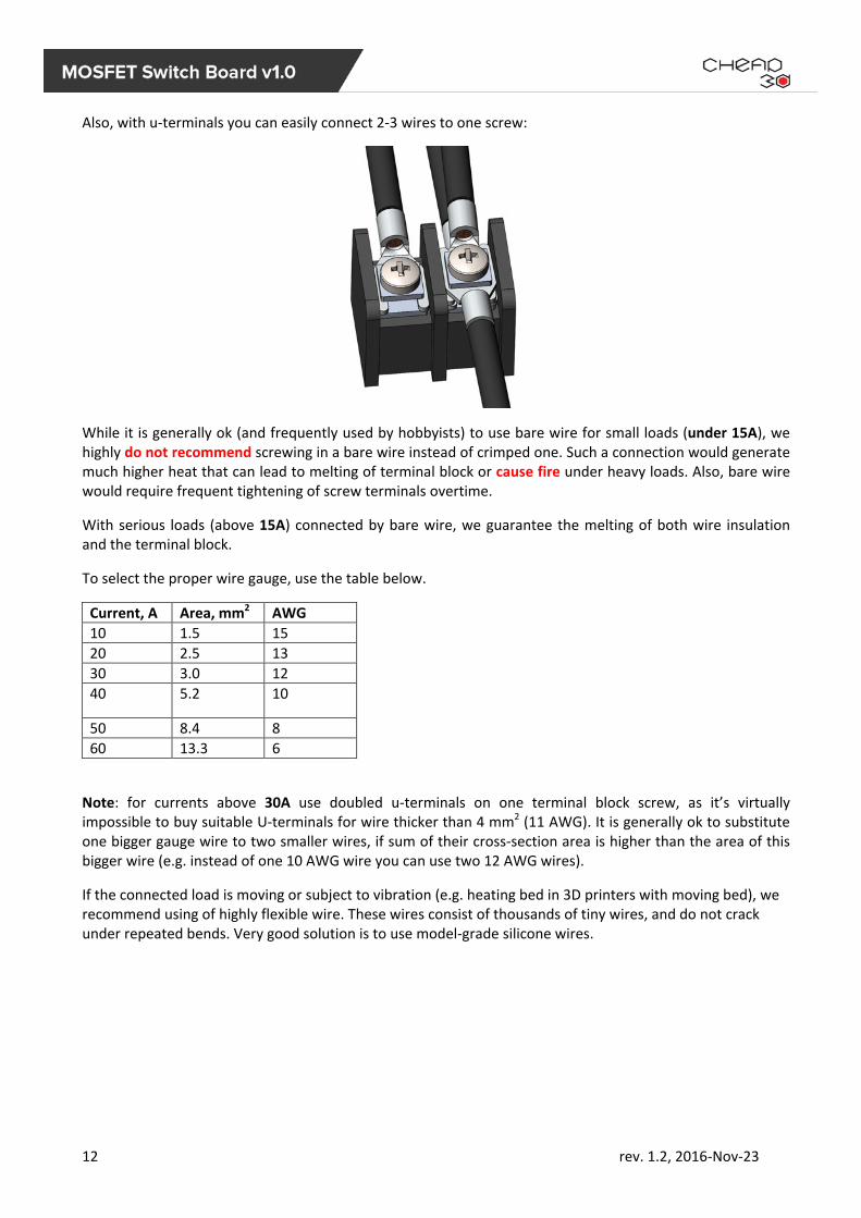
Also, with u-terminals you can easily connect 2-3 wires to one screw:
While it is generally ok (and frequently used by hobbyists) to use bare wire for small loads (under 15A), we highly do not recommend screwing in a bare wire instead of crimped one. Such a connection would generate much higher heat that can lead to melting of terminal block or cause fire under heavy loads. Also, bare wire would require frequent tightening of screw terminals overtime.
With serious loads (above 15A) connected by bare wire, we guarantee the melting of both wire insulation and the terminal block.
To select the proper wire gauge, use the table below.
Note: for currents above 30A use doubled u-terminals on one terminal block screw, as it’s virtually impossible to buy suitable U-terminals for wire thicker than 4 mm2 (11 AWG). It is generally ok to substitute one bigger gauge wire to two smaller wires, if sum of their cross-section area is higher than the area of this bigger wire (e.g. instead of one 10 AWG wire you can use two 12 AWG wires).
If the connected load is moving or subject to vibration (e.g. heating bed in 3D printers with moving bed), we recommend using of highly flexible wire. These wires consist of thousands of tiny wires, and do not crack under repeated bends. Very good solution is to use model-grade silicone wires.
13 rev. 1.2, 2016-Nov-23
6 Nerd zone: Testing results and Graphs
Fig. 3. Board Temperature vs. Load Current, without fan
Fig. 4. Board Temperature vs. Load Current with fan
14 rev. 1.2, 2016-Nov-23
Fig. 5. Pulsed current duration
Fig. 6. Maximum PWM Frequency vs Current, single channel active
*The frequencies above 4000 Hz are not tested.
15 rev. 1.2, 2016-Nov-23
Fig. 7. Input Sink Current vs Input Logic Voltage
Fig. 8. MOSFET Switching waveforms
16 rev. 1.2, 2016-Nov-23
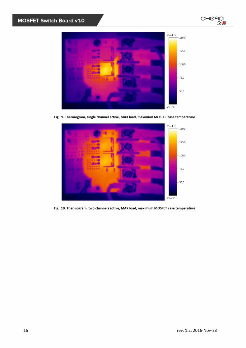
Fig. 9. Thermogram, single channel active, MAX load, maximum MOSFET case temperature
Fig. 10. Thermogram, two channels active, MAX load, maximum MOSFET case temperature
17 rev. 1.2, 2016-Nov-23
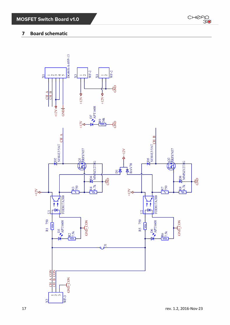
7 Board schematic
18 rev. 1.2, 2016-Nov-23
8 Board dimensions (all units in mm)
19 rev. 1.2, 2016-Nov-23
9 Errata
There is no known errata for this board.
10 Revision History
Version Date Changes rev. 1.0 2016-Sep-08 Initial release rev. 1.1 2016-Nov-02 Increased CH_A/CH_B inputs to logic GND maximum voltage and
CH_A/CH_B inputs sink current rev. 1.2 2016-Nov-23 Added a full connection diagram for Cheap3D V300 3D printer.
Added compatible terminals for barrier terminal block.