Top-Gate Thin Film Transistor with ZnO:N Channel Fabricated by Room Temperature RF Magnetron Sputtering
Meng Zhang, Wei Zhou, Rongsheng Chen, Man Wong and Hoi-Sing Kwok State Key Lab on Advanced Displays and Optoelectronics,
The Hong Kong University of Science and Technology, Clear Water Bay, Kowloon, Hong Kong
Abstract In this work, top-gate thin film transistor (TFT) with ZnO doped nitrogen (ZnO:N) channel fabricated by room temperature rf magnetron sputtering is demonstrated. ZnO:N film is obtained by introducing N2 ambient when sputtering ZnO. The crystallization of ZnO:N is better compared to ZnO film. The test results indicate that the ZnO:N could improve the electrical characteristics as an active channel layer for a TFT device. This in-process doping method may be a valuable technique for the fabrication of the practical and stable TFT devices.
Keywords: ZnO, ZnO:N, thin film transistor, room temperature sputtering
1. Introduction Metal oxide based thin film transistor (TFT) has been hotly pursued for display and other applications due to its transparency [1], high on/off current ratio [2], relatively low processing temperature [3] and low cost [4]. Among metal oxide candidates, zinc oxide (ZnO) has received a lot of attention because ZnO can be directly deposited in the polycrystalline phase even at room temperature [3, 4]. Therefore, it is compatible with plastic and/or flexible displays [5]. To improve the performance of ZnO TFTs, several methods [4-8] have been applied, such as plasma treatment [6], post annealing [7], high-k dielectric [8] and novel structure [4]. Additionally, most reported ZnO TFTs were fabricated by using a bottom-gate configuration, which means the initial growth layer of ZnO would serve as the active channel of TFTs. The crystal defect in the initial ZnO layer is more than that in the bulk [4]. Thus high mobility is expected in the top-gate configuration rather than the bottom-gate configuration [4]. In this work, top-gate TFT with ZnO doped nitrogen (ZnO:N) channel fabricated by room temperature rf magnetron sputtering is demonstrated. By introducing N2 gas when sputtering ZnO, ZnO:N is obtained. TFT employing such ZnO:N as channel exhibits better electrical performance in terms of mobility, threshold voltage and on/off ratio.
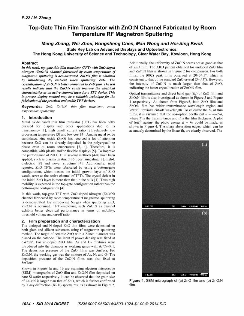
2. Film preparation and characterization The undoped and N doped ZnO thin films were deposited on both glass and silicon substrates using rf magnetron sputtering method. The target of ceramic ZnO with a 2-inch diameter was placed on the cathode. The input rf power density was fixed at 6W/cm2. For un-doped ZnO film, Ar and O2 mixtures were introduced into the chamber as working gases with Ar/O2=9:1. The deposition pressure of the ZnO films was 5mTorr. For ZnO:N, the working gas was the mixture of Ar, N2 and O2 The deposition pressure of the ZnO:N films was also fixed at 5mTorr. Shown in Figure 1a and 1b are scanning electron microscope (SEM) micrographs of ZnO film and ZnO:N film deposited on bare Si wafer respectively. It can be observed that the grain size of ZnO:N is larger than that of ZnO, which is further confirmed by X-ray diffraction (XRD) spectra results as shown in Figure 2.
Additionally, the uniformity of ZnO:N seems not as good as that of ZnO film. The XRD pattern obtained for undoped ZnO film and ZnO:N film is shown in Figure 2 for comparison. For both films, the (002) peak in is observed at 2θ≈34.5°, which is consistent to that of the standard ZnO crystal (34.45°). However, the intensity of ZnO:N is much larger than that of ZnO, indicating the better crystallization of ZnO:N film. Optical transmittance and direct band gap (Eg) of ZnO film and ZnO:N film is also investigated as shown in Figure 3 and Figure 4 respectively. As shown from Figure3, both ZnO film and ZnO:N film has wider transmittance wavelength region and lower ultraviolet cut-off wavelength. To calculate the Eg of thin films, it is assumed that the absorption coefficient α = ‒lnT/d, where T is the transmittance and d is the film thickness. A plot of (αE)2 against the photo energy E = hν could be made, as shown in Figure 4. The sharp absorption edges, which can be accurately determined by the linear fit, are clearly observed. The
Figure 1. SEM micrograph of (a) ZnO film and (b) ZnO:N film.
Figure 2. Comparison of XRD spectra of ZnO film and ZnO:N film.
300 400 500 600 700 800 900 10000
20
40
60
80
100
Tran
smitt
ance
(%)
Wavelength (nm)
Glass substrate ZnO film ZnO:N film
Figure 3. The transmittance of ZnO film and ZnO:N film as a function of the wavelength.
Eg of ZnO and ZnO:N determined from the obtained absorption spectra are 3.30eV and 3.37eV respectively. The Eg of ZnO:N is slightly larger than that of ZnO. Here, the addition of N may suppress the oxygen vacancy formation, increasing the optical Eg while sharping the Urbach tail and thus reducing the density of subgap defect states [9]. X-ray photoelectron spectroscopy (XPS) spectrums of ZnO film and ZnO:N film in the O 1s binding energy region are shown in Figure 5. The red line represents for ZnO film while the blue line represents for ZnO:N film. Compared to ZnO film, there is a slightly negative shift (~0.2eV) in binding energy for ZnO:N film. This small difference between ZnO and ZnO:N may be attributed to the doping of N. Shown in Figure 6 are the XPS spectrums of ZnO film and ZnO:N film in the N 1s binding
energy region. The broad peak of ZnO:N is around 397eV, which is consistent to reported atomic layer deposition ZnO in situ doped N [5]. From the peak intensity, the N concentration in ZnO:N film is estimated to be around 1.21 at. %. The N concentration in ZnO film is less than 0.12 at. %. By additionally introducing N2 ambient when sputtering ZnO film, N is lightly incorporated into the film, resulting ZnO:N. This small portion of N atoms is considered to compensate the n-type carriers [5].
2.5 2.6 2.7 2.8 2.9 3.0 3.1 3.2 3.3 3.4 3.5 3.6
1
2
3
4
5
(E)
2
(c
m2
eV2 )
E (ev)
ZnO film ZnO:N film
Figure 4. The Eg of ZnO film and ZnO:N film determined from the absorption spectra. The Eg of ZnO and ZnO:N are 3.30eV and 3.37eV respectively.
2x10⁴
3x10⁴
4x10⁴
5x10⁴
6x10⁴
526 528 530 532 534 536 538 540
Inte
nsity
(a.u
.)
O 1s in ZnO film
Binding energy (eV)
O 1s in ZnO:N film
Figure 5. XPS spectrum in O 1s binding energy region of ZnO film and ZnO:N film.
P-22 / M. Zhang
SID 2014 DIGEST • 1025
386 388 390 392 394 396 398 400 402 404 406
3000
3500
4500
N 1s in ZnO film In
tens
ity (a
.u.)
Binding energy (eV)
N 1s in ZnO:N film
Figure 6. XPS spectrum in N 1s binding energy region of ZnO film and ZnO:N film.
3. Device fabrication and characterization
Figure 7. Schematic of top-gate ZnO:N TFTs fabrication process flow.
Shown in Figure 7 Schematic of top-gate ZnO:N TFTs fabrication process flow. First, 500nm thermal oxide was grown on 4-inch c-Si wafers in furnace. Then 100nm ITO source/drain was deposited using lift-off process, followed by ZnO film and ZnO:N deposition. After ZnO film and ZnO:N deposition, 50nm SiO2 was deposited serving as etching stop layer and gate dielectric. Then active layer pattern was performed using SiO2 dry etching process and ZnO/ZnO:N wet etching process. After definition of active layer, another 100nm SiO2 was deposited as gate dielectric. The total thickness of gate dielectric is 150nm. Next, 100nm ITO gate electrode was deposited again using lift-off process. Finally 200nm SiO2 was deposited as passivation l-
0 5 10 15 20
0
5
10
15
20
25
Gate voltage (V)
ZnO TFT ZnO:N TFT
W/L = 50/25 mVds = 5V
Dra
in c
urre
nt (
A)
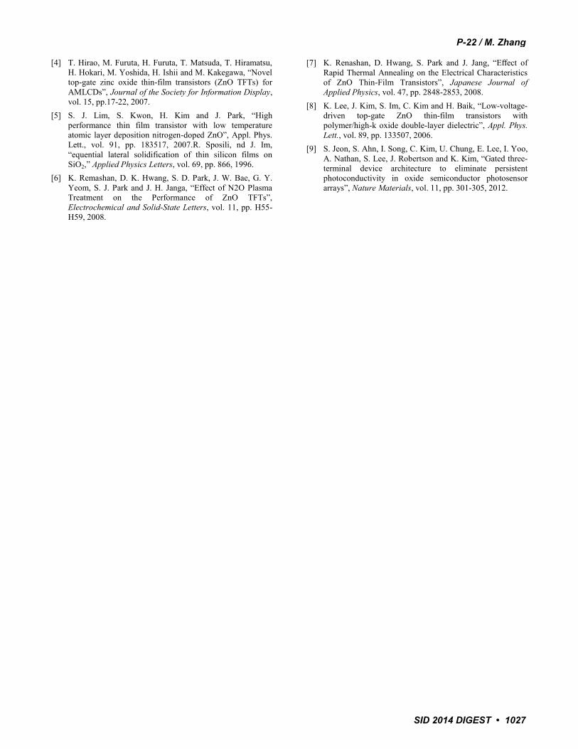
Figure 8. Transfer curves of ZnO TFTs and ZnO:N TFT at Vds = 5V. -ayer. The width, length, and overlap of source/drain and gate in these TFT devices are 50, 25, and 5μm, respectively. The Agilent 4156A semiconductor parameter analyzer is used to test the devices. Shown in Figure 8 is transfer curve comparison between ZnO TFTs and ZnO:N TFT measured at Vds = 5V. Device parameters are improved by ZnO:N TFT, compared to ZnO TFTs, especially for on current. The field effect mobility increases from 1.9 cm2/Vs to 16.1 cm2/Vs. The on/off ratio increases from 9.22×10⁵ to 8.19×10⁶. The improvement may be attributed to high crystallization quality of ZnO:N and passivation of O vacancy by N atoms [5].
4. Conclusion In this work, top-gate TFT with ZnO:N channel fabricated by room temperature rf magnetron sputtering is demonstrated. By introducing N2 gas when sputtering ZnO, ZnO:N is successfully obtained. By characterizing ZnO:N film, it is found that crystallization quality of ZnO:N is better than that of ZnO. TFT employing such ZnO:N as active channel exhibits better electrical performance.
5. Acknowledgement This work was supported by Hong Kong Government Research Grants Council Theme-Based Research Scheme under Grant T23-713/11-1.
6. References [1] Z. Ye, L. Lu and M. Wong, “Zinc-Oxide Thin Film
Transistor with Self-Aligned Source/Drain Regions Doped With Implanted Boron for Enhanced Thermal Stability”, IEEE Trans. Electron Devices, vol. 59, pp. 393-399, 2004.
[2] B. Bayraktaroglu, K. Leedy and R. Neidhard, “High-Frequency ZnO Thin-Film Transistors on Si Substrates”, IEEE Electron Device Lett., vol. 30, pp. 946-948, 2009.
[3] E. M. C. Fortunato, P. M. C. Barquinha, A. C. M. B. G. Pimentel, A. M. F. Gonçalves, A. J. S. Marques, L. M. N. Pereira and R. F. P. Martins, “Fully Transparent ZnO Thin-Film Transistor Produced at Room Temperature”, Advanced Materials, vol. 17, pp.590-594, 2005.
P-22 / M. Zhang
1026 • SID 2014 DIGEST
[4] T. Hirao, M. Furuta, H. Furuta, T. Matsuda, T. Hiramatsu, H. Hokari, M. Yoshida, H. Ishii and M. Kakegawa, “Novel top-gate zinc oxide thin-film transistors (ZnO TFTs) for AMLCDs”, Journal of the Society for Information Display, vol. 15, pp.17-22, 2007.
[5] S. J. Lim, S. Kwon, H. Kim and J. Park, “High performance thin film transistor with low temperature atomic layer deposition nitrogen-doped ZnO”, Appl. Phys. Lett., vol. 91, pp. 183517, 2007.R. Sposili, nd J. Im, “equential lateral solidification of thin silicon films on SiO2,” Applied Physics Letters, vol. 69, pp. 866, 1996.
[6] K. Remashan, D. K. Hwang, S. D. Park, J. W. Bae, G. Y. Yeom, S. J. Park and J. H. Janga, “Effect of N2O Plasma Treatment on the Performance of ZnO TFTs”, Electrochemical and Solid-State Letters, vol. 11, pp. H55-H59, 2008.
[7] K. Renashan, D. Hwang, S. Park and J. Jang, “Effect of Rapid Thermal Annealing on the Electrical Characteristics of ZnO Thin-Film Transistors”, Japanese Journal of Applied Physics, vol. 47, pp. 2848-2853, 2008.
[8] K. Lee, J. Kim, S. Im, C. Kim and H. Baik, “Low-voltage-driven top-gate ZnO thin-film transistors with polymer/high-k oxide double-layer dielectric”, Appl. Phys. Lett., vol. 89, pp. 133507, 2006.
[9] S. Jeon, S. Ahn, I. Song, C. Kim, U. Chung, E. Lee, I. Yoo, A. Nathan, S. Lee, J. Robertson and K. Kim, “Gated three-terminal device architecture to eliminate persistent photoconductivity in oxide semiconductor photosensor arrays”, Nature Materials, vol. 11, pp. 301-305, 2012.