Performances of the COROT CCDs for high accuracy photometry Pernelle Bernardi and the CCD team From Meudon : Tristan Buey, Vincent Lapeyrere, Régis Schmidt, Bertrand le Ruyet, Jêrome Parisot, Didier Tiphène From CNES : Olivier Gilard, Guy Rolland (for irradiation tests) 2 nd Eddington Worskshop, Mondello (Italy), 9-11 April 2003
Transcript
Performances of the COROT CCDs for high accuracy photometry
Pernelle Bernardi
and the CCD teamFrom Meudon : Tristan Buey, Vincent Lapeyrere, Régis Schmidt, Bertrand le Ruyet,
Jêrome Parisot, Didier Tiphène
From CNES : Olivier Gilard, Guy Rolland (for irradiation tests)
2nd Eddington Worskshop, Mondello (Italy), 9-11 April 2003
2nd Eddington Workshop, Mondello, 9-11 April 2003
2
Corot CCD
• E2V 42-80
• Back-thinned, MPP, anti-reflection coating
• Operating in frame transfer mode
• Size of image area : 2048 rows, 2048 columns
• Pixel pitch: 13.5µm
• 2 outputs, dump drain register
• Readout frequency: 100kHz
• Readout timing: 100µs to transfer a row from the image area to the storage area
150µs to transfer a row in the register
• Three sides buttable
No specific technological developments
Space qualification
2nd Eddington Workshop, Mondello, 9-11 April 2003
3
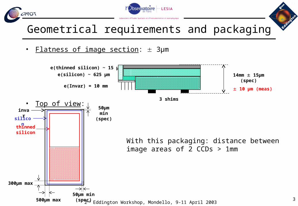
Geometrical requirements and packaging
• Flatness of image section: 3µm
• Top of view:
14mm 15µm (spec)
10 µm (meas)e(Invar) = 10 mm
e(silicon) ~ 625 µm
e(thinned silicon) ~ 15 µm
3 shims
silicon
invar
thinned silicon
50µm min (spec)
50µm min (spec)
500µm max
300µm max
With this packaging: distance between image areas of 2 CCDs > 1mm
2nd Eddington Workshop, Mondello, 9-11 April 2003
4
Working point
• 3 bias voltages are optimised: VOD, VRD, VOG
• Working range: measurement of the video signal for different values of the bias voltages
5 CCDs have the same working ranges for the 3 bias voltages
1 has a different behaviour: excluded from the flight
Video signal vs Vod
20000
30000
40000
50000
60000
70000
80000
90000
100000
1800 2300 2800 3300
Vod (ADU)
Left output
Right output
• Sensitivity of the video signal to the bias voltages :
About same order at worst frequency (100kHz, readout frequency). Higher sensitivities = 4e-/mV Specification for the electronics: 1mV peak to peak ---> equivalent noise of few e-.
2nd Eddington Workshop, Mondello, 9-11 April 2003
5
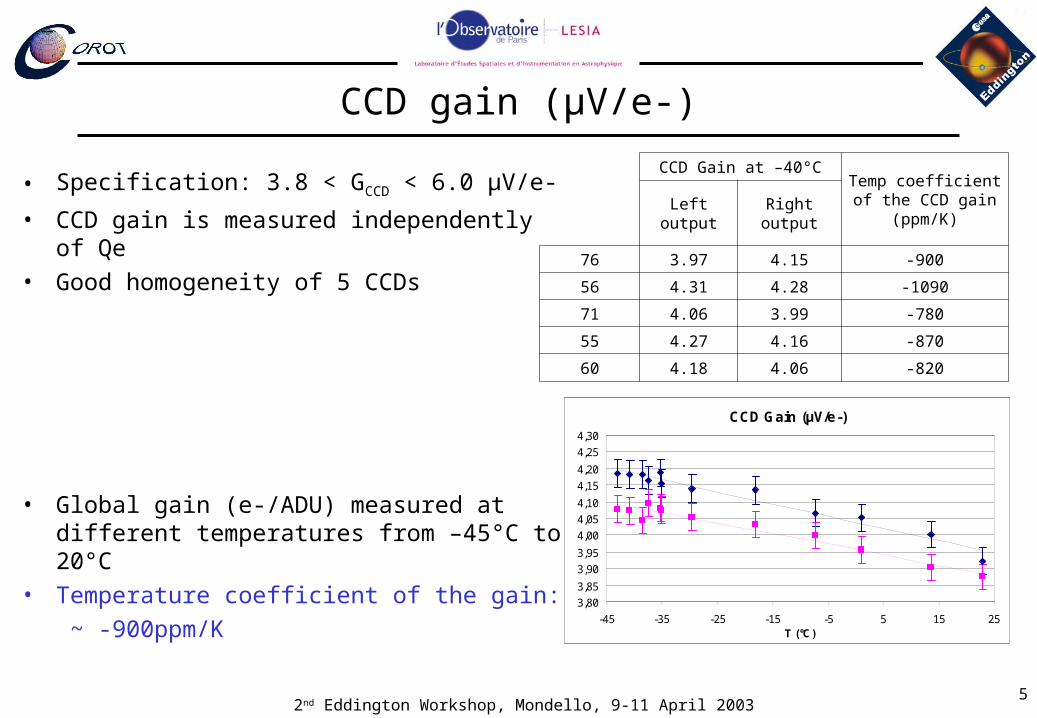
CCD gain (µV/e-)
• Specification: 3.8 < GCCD < 6.0 µV/e-
• CCD gain is measured independently of Qe
• Good homogeneity of 5 CCDs
• Global gain (e-/ADU) measured at different temperatures from –45°C to 20°C
• Temperature coefficient of the gain:
~ -900ppm/K
CCD Gain at –40°CTemp coefficient of
the CCD gain (ppm/K)Left output Right output
76 3.97 4.15 -900
56 4.31 4.28 -1090
71 4.06 3.99 -780
55 4.27 4.16 -870
60 4.18 4.06 -820
CCD Gain (µV/e-)
3,80
3,85
3,90
3,95
4,00
4,05
4,10
4,15
4,20
4,25
4,30
-45 -35 -25 -15 -5 5 15 25T (°C)
2nd Eddington Workshop, Mondello, 9-11 April 2003
6
Quantum Efficiency
• E2V data: Qe max = 0.90 at 650nm
average Qe = 0.62
• Temperature coefficient of Qe:
– Measure of the flux at:
- different wavelengths from 400nm to 1000nm
- different temperatures from –45°C to –30°C
– Calculation of the temperature coefficient of the CCD response
– Correction by the temperature coefficient of the CCD gain (G ~ -900ppm/K)
Temperature coefficient of Qe ~ 2000ppm/K for the center of the bandwith
Quantum Efficiency
0
10
20
30
40
50
60
70
80
90
100
200 300 400 500 600 700 800 900 1000
Wavelength (nm)
Qe
(%)
Temperature coefficient of Quantum Efficiency
0
1000
2000
3000
4000
5000
6000
7000
8000
9000
400 500 600 700 800 900 1000
Wavelength (nm)
DQ
e/Q
e (p
pm
/K)
2nd Eddington Workshop, Mondello, 9-11 April 2003
7
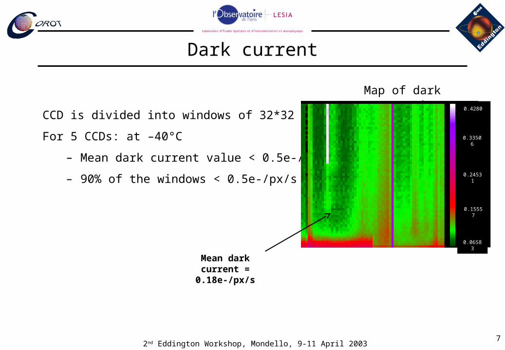
Dark current
CCD is divided into windows of 32*32 pixels
For 5 CCDs: at –40°C
– Mean dark current value < 0.5e-/px/s
– 90% of the windows < 0.5e-/px/s
Map of dark current
0.4280
0.33506
0.24531
0.15557
0.06583
Mean dark current = 0.18e-/px/s
2nd Eddington Workshop, Mondello, 9-11 April 2003
8
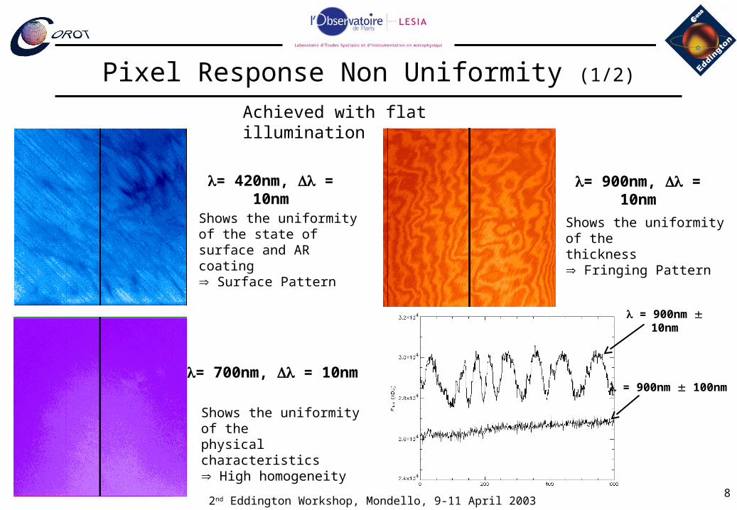
Pixel Response Non Uniformity (1/2)
= 420nm, D = 10nm
= 700nm, D = 10nm
= 900nm, D = 10nm
Achieved with flat illumination
Shows the uniformityof the state of surface and AR coating Surface Pattern
Shows the uniformity of the physical characteristics High homogeneity
Shows the uniformity of the thickness Fringing Pattern
= 900nm 10nm
= 900nm 100nm
2nd Eddington Workshop, Mondello, 9-11 April 2003
9
Pixel Response Non Uniformity (2/2)
• CCD is divided into windows of 32*32 pixels.
• Local PRNU = dispersion of the pixel response in a 32*32 pixel window.
• For 5 CCDs: local PRNU is 5 times lower than specification.
• Stable with temperature
Local PRNU
0,00
0,50
1,00
1,50
2,00
2,50
450 550 650 750 850Wavelength (nm )
76
56
71
55
60
2nd Eddington Workshop, Mondello, 9-11 April 2003
10
Cosmetics
• Definitions:– White spot: > 100e-/px/s at –40°C– Black spot: when pixel response is less than 50% of the local mean response, at -40°C.– Column defect: more than 100 contiguous blemish elements (white and black spots)
• Specifications:– Less than 750 black and white spots– Less than 6 column defects
• Measurements: specifications are fullfilled– 5 CCDs have no white spots, 1 CCD has 2 white spots– The worst CCD has 2 columns defects (black columns)
2nd Eddington Workshop, Mondello, 9-11 April 2003
11
Maps of defects
• 2 maps calculated per CCD: one for each scientific program.– Images of dark current and flat fields in three parts of the bandwith– 2 shapes of PSF (seismo and exoplanets)– Performances of the instrument for each program
Seismology channel Exoplanet channel
Same CCD
2nd Eddington Workshop, Mondello, 9-11 April 2003
12
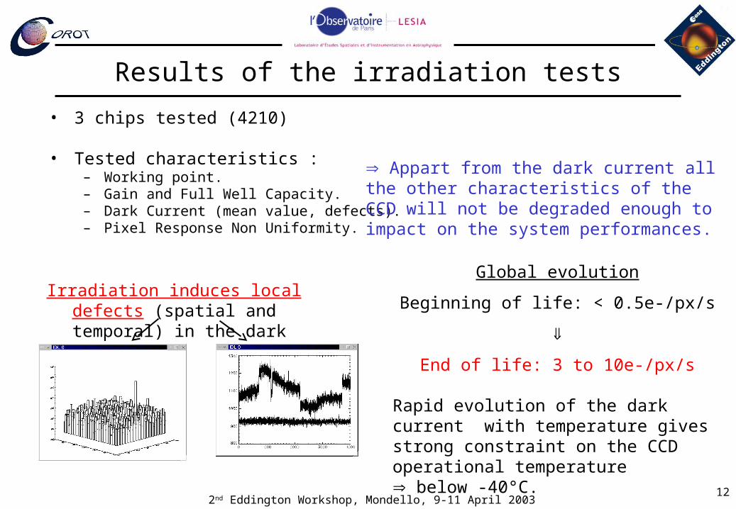
Results of the irradiation tests
• 3 chips tested (4210)
• Tested characteristics :– Working point.– Gain and Full Well Capacity.– Dark Current (mean value, defects).– Pixel Response Non Uniformity.
Irradiation induces local defects (spatial and temporal) in the dark current
Global evolution
Beginning of life: < 0.5e-/px/s
End of life: 3 to 10e-/px/s
Rapid evolution of the dark current with temperature gives strong constraint on the CCD operational temperature below -40°C.
Appart from the dark current all the other characteristics of the CCD will not be degraded enough to impact on the system performances.
2nd Eddington Workshop, Mondello, 9-11 April 2003
13
Conclusion
• Sixth CCD currently under tests
• Calibration of 10 CCDs FM will be finished before summer
• Then: sort the 10 CCDs
select 4 CCDs for the flight using software tools
• If necessary, some specific measurements can be done on selected CCDs


![07 | La Maison Standar de Jean Prouvé en Meudon. Edificio ... · 107 ISSN: 2340-9711 rita_02 | oct 2014 [1] Situación y emplazamiento de las Maisons de Meudon. de chapa de acero](https://static.documents.pub/doc/80x56/5d41e82188c9936e348c7b55/07-la-maison-standar-de-jean-prouve-en-meudon-edificio-107-issn-2340-9711.jpg)


