POSITION ESTIMATION AND GAP MEASUREMENT OF A POINT MACHINE USING AN ELECTRONIC DEVICE WITH EMBEDDED ARTIFICIAL VISION FIRMWARE A Master's Thesis Submitted to the Faculty of the Escola Tècnica d'Enginyeria de Telecomunicació de Barcelona Universitat Politècnica de Catalunya by Rafel Mormeneo Melich In partial fulfillment of the requirements for the degree of MASTER OF SCIENCE IN RESEARCH ON INFORMATION AND COMMUNICATION TECHNOLOGIES Advisor: Javier Ruiz Hidalgo Barcelona, June 2015
Transcript
POSITION ESTIMATION AND GAP MEASUREMENT OF A
POINT MACHINE USING AN ELECTRONIC DEVICE WITH
EMBEDDED ARTIFICIAL VISION FIRMWARE
A Master's Thesis
Submitted to the Faculty of the
Escola Tècnica d'Enginyeria de Telecomunicació de
Barcelona
Universitat Politècnica de Catalunya
by
Rafel Mormeneo Melich
In partial fulfillment
of the requirements for the degree of
MASTER OF SCIENCE IN RESEARCH ON INFORMATION
AND COMMUNICATION TECHNOLOGIES
Advisor: Javier Ruiz Hidalgo
Barcelona, June 2015
1
Title of the thesis: Position estimation and gap measurement of a point machine
using an electronic device with embedded artificial vision firmware
Author: Rafel Mormeneo Melich
Advisor: Javier Ruiz Hidalgo
Abstract
An electronic device based on a microcontroller and an image sensor is designed and developed. The device will be used in the railway sector to monitor the current position of a point machine and the gap between two mechanical parts inside it. It has to improve and resolve some issues of other devices in the market that perform the same task but with different technologies. Embedded firmware for the device has been developed to process images to estimate the position of the point machine and the above mentioned gap. The device will transmit the information and, eventually, images to a central server which stores the information of all devices in the system. Accuracy and precision of the measurements are presented. We will also compare the measures between the new device and the previous one to validate the improvement.
2
I dedicate this dissertation to my family who has encouraged me all the time, specially to
my wife, Elisabeth who has helped me a lot in the final sprint.
3
Acknowledgements
Thank you very much to all the team of Thinking Forward XXI with whom I have been
working side by side during the last four years. All together we have done a great work
that has allowed us to develop and produce this new device.
I also want to acknowledge Marc because he has given me some drawings that I have
used in this document and everybody who has helped me to review it: Aida, Jessica, Ezio
and Żaneta.
My wife, Elisabeth, also merits some acknowledgment words not only by giving me
emotional support but also by understanding me in those moments when I was absorbed
and I could not devote her all the attention she deserves.
Finally, I want to acknowledge Javier, who gave me some valuable advice, supervised
my work was always pushing me to finish this work.
4
Revision history and approval record
Revision Date Purpose
0 23/03/2015 Document creation
1 06/05/2015 Preliminary Revision
2 08/06/2015 Complete Revision
3 22/06/2015 Final Revision
Written by: Reviewed and approved by:
Date 14/06/2015 Date 22/06/2015
Name Rafel Mormeneo Melich Name Javier Ruiz Hidalgo
Position Project Author Position Project Supervisor
Figure 51. Standard deviation of the measures ................................................................. 63
Figure 52. BOM Cost distribution ....................................................................................... 65
Figure 53. Remote installation program ............................................................................. 68
9
List of Tables
Table 1. Example of calibration points ............................................................................... 19
Table 2. DOE Pattern angles and computed pattern size at 150mm distance ................. 31
Table 3. Implemented erode function ................................................................................ 43
Table 4. Implemented dilate function ................................................................................. 43
Table 5. Errors of the measurements in millimeters. u=upper bar, l=lower bar ................ 62
Table 6. Standard deviation ............................................................................................... 63
Table 7. Bill of Materials ..................................................................................................... 65
Table 8. Personal Costs ..................................................................................................... 66
10
1. Introduction
1.1. Summary
The present project has been developed in a company called Thinking Forward XXI (TF).
I have been working in TF during the last four years and at the same time I was coursing
the Master MERIT.
In TF we developed a monitoring device to build a failure predictive system for electric
engines in the railway sector which has been patented with patent number
ES2374465(B1), [3]. One of the sensors of this device monitors a gap between two
mechanical parts by using magnets and magnetic field sensors. We have to monitor the
gap in one degree of freedom, but the magnetic field sensor is sensible to a 3D magnetic
field. This causes the system to give bad measurements quite often. When we analyzed
this problem I was taking an image processing course of the Master MERIT and I
proposed to use a computer vision based device to substitute the magnetic field sensor.
After studying the proposal we found that it was the best solution to avoid the problems of
the previous device.
This project contains the whole design and development of an image based sensor. This
sensor monitors a gap between two mechanical parts of a point machine that operates a
railway switch. A railway switch and a point machine description and functionality can be
found in Section 1.2. The device has been integrated in the monitoring system developed
in TF with other devices which monitor electric and environmental parameters of point
machines.
Basically, the device captures and analyses an image to determine the position of the
point machine, it can be in two positions as we will see in the next section, and the gap
between these two parts which also will be explained in the next section. The device has
a microcontroller with an embedded firmware that processes the image to perform the
analysis. First, the image is binarized using a statistical method. Then the binary map is
filtered with a morphological and a geometrical filter taking into account the geometry of
the monitored area. Then we extract objects from the image by labeling the connected
components. After that, the position of the point machine is determined by looking at
some regions of interest (ROI) in the image and finally the gap is estimated directly over
the image and transformed to a measure in millimeters using a known element in the
image.
The document is structured as follows. In Section 1.2 we expose the field of application of
the developed device and then in Section 1.3 we explain the goals and specifications of
the project. A brief look at the project planning can be found in Section 1.4. In Chapter 2
we can find the state of the art regarding industrial applications which use computer
vision to perform some tasks, embedded systems that performs image processing tasks
and finally the previous work done in Thinking Forward XXI with the monitoring and
predictive system. In Chapter 3 we will expose the fundamentals of the image algorithms
used in this project. Next, in Chapter 4 we can find the design and development of the
device and its integration in the system. In Chapter 5 we present some results of the
device. In Chapter 6 there is a summary of the costs of the project. Finally in Chapter 7
we present the conclusions and future work that can be done to improve the developed
device.
11
1.2. Field of application
This project relates to an industrial monitoring system. More specifically the main
application of the developed device is to monitor, in real time, the position of a point
machine.
A point machine is an electric motor driven switch that enables an operator to switch a
train from one railroad track to another. The main elements of a switch are the points.
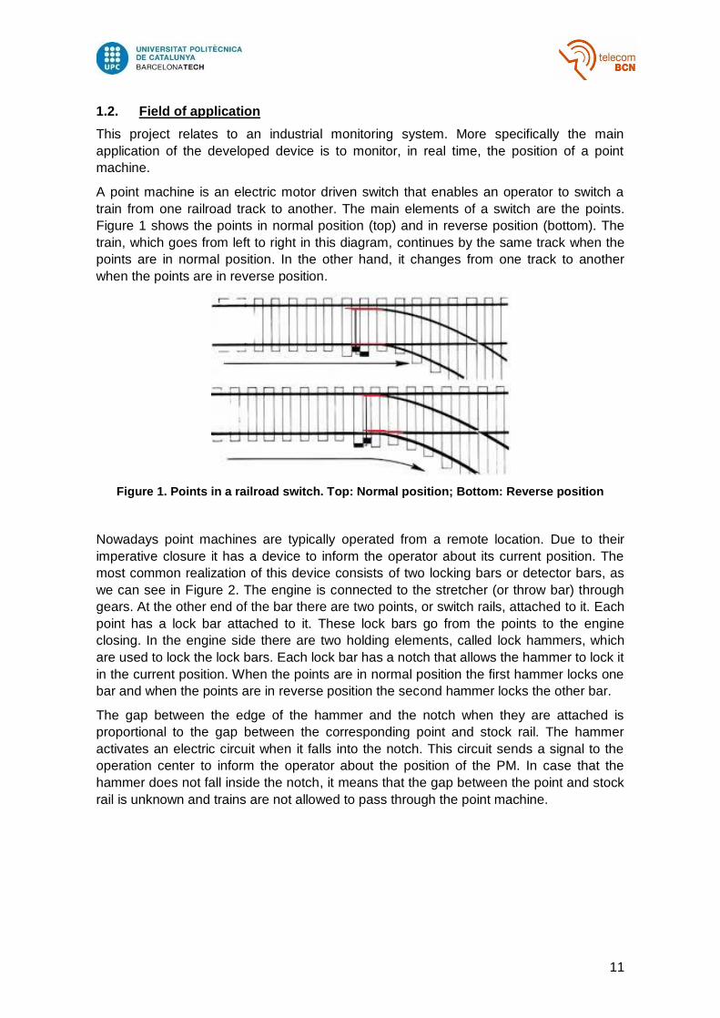
Figure 1 shows the points in normal position (top) and in reverse position (bottom). The
train, which goes from left to right in this diagram, continues by the same track when the
points are in normal position. In the other hand, it changes from one track to another
when the points are in reverse position.
Figure 1. Points in a railroad switch. Top: Normal position; Bottom: Reverse position
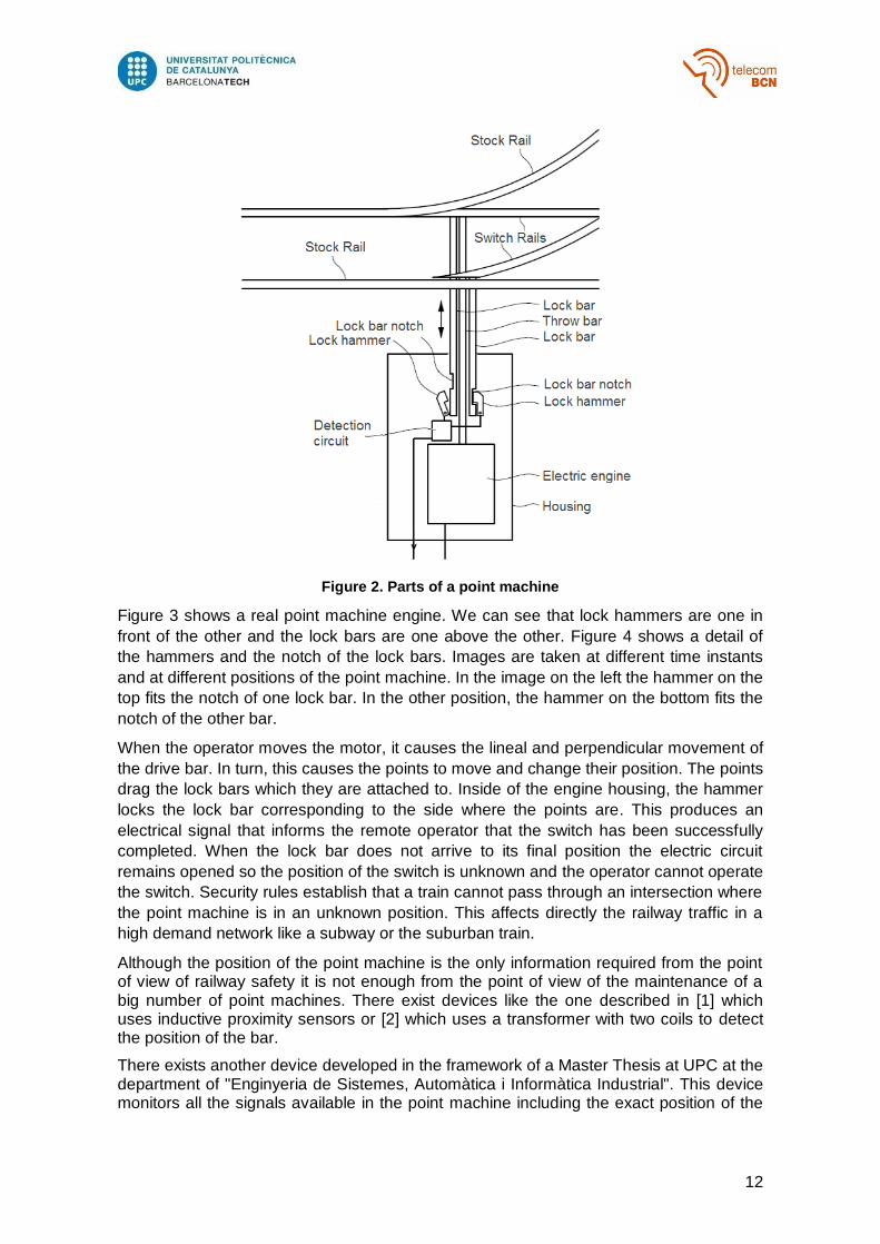
Nowadays point machines are typically operated from a remote location. Due to their
imperative closure it has a device to inform the operator about its current position. The
most common realization of this device consists of two locking bars or detector bars, as
we can see in Figure 2. The engine is connected to the stretcher (or throw bar) through
gears. At the other end of the bar there are two points, or switch rails, attached to it. Each
point has a lock bar attached to it. These lock bars go from the points to the engine
closing. In the engine side there are two holding elements, called lock hammers, which
are used to lock the lock bars. Each lock bar has a notch that allows the hammer to lock it
in the current position. When the points are in normal position the first hammer locks one
bar and when the points are in reverse position the second hammer locks the other bar.
The gap between the edge of the hammer and the notch when they are attached is
proportional to the gap between the corresponding point and stock rail. The hammer
activates an electric circuit when it falls into the notch. This circuit sends a signal to the
operation center to inform the operator about the position of the PM. In case that the
hammer does not fall inside the notch, it means that the gap between the point and stock
rail is unknown and trains are not allowed to pass through the point machine.
12
Figure 2. Parts of a point machine
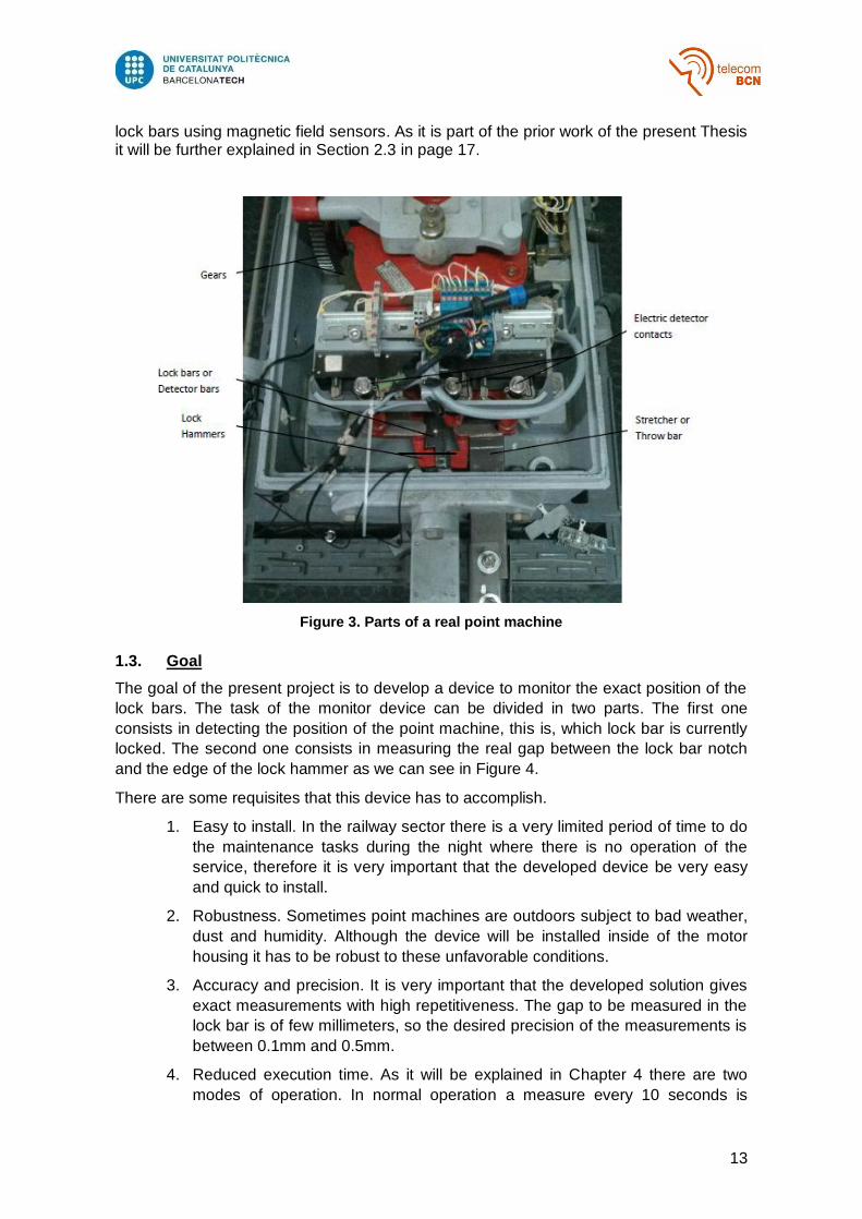
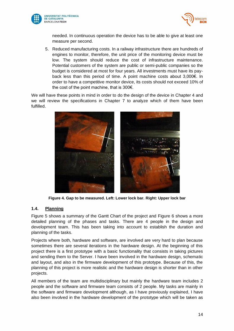
Figure 3 shows a real point machine engine. We can see that lock hammers are one in
front of the other and the lock bars are one above the other. Figure 4 shows a detail of
the hammers and the notch of the lock bars. Images are taken at different time instants
and at different positions of the point machine. In the image on the left the hammer on the
top fits the notch of one lock bar. In the other position, the hammer on the bottom fits the
notch of the other bar.
When the operator moves the motor, it causes the lineal and perpendicular movement of
the drive bar. In turn, this causes the points to move and change their position. The points
drag the lock bars which they are attached to. Inside of the engine housing, the hammer
locks the lock bar corresponding to the side where the points are. This produces an
electrical signal that informs the remote operator that the switch has been successfully
completed. When the lock bar does not arrive to its final position the electric circuit
remains opened so the position of the switch is unknown and the operator cannot operate
the switch. Security rules establish that a train cannot pass through an intersection where
the point machine is in an unknown position. This affects directly the railway traffic in a
high demand network like a subway or the suburban train.
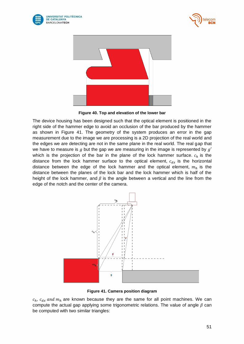
Although the position of the point machine is the only information required from the point of view of railway safety it is not enough from the point of view of the maintenance of a big number of point machines. There exist devices like the one described in [1] which uses inductive proximity sensors or [2] which uses a transformer with two coils to detect the position of the bar.
There exists another device developed in the framework of a Master Thesis at UPC at the department of "Enginyeria de Sistemes, Automàtica i Informàtica Industrial". This device monitors all the signals available in the point machine including the exact position of the
13
lock bars using magnetic field sensors. As it is part of the prior work of the present Thesis it will be further explained in Section 2.3 in page 17.
Figure 3. Parts of a real point machine
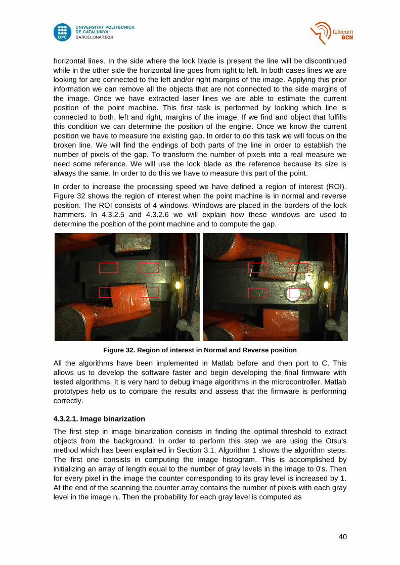
1.3. Goal
The goal of the present project is to develop a device to monitor the exact position of the
lock bars. The task of the monitor device can be divided in two parts. The first one
consists in detecting the position of the point machine, this is, which lock bar is currently
locked. The second one consists in measuring the real gap between the lock bar notch
and the edge of the lock hammer as we can see in Figure 4.
There are some requisites that this device has to accomplish.
1. Easy to install. In the railway sector there is a very limited period of time to do
the maintenance tasks during the night where there is no operation of the
service, therefore it is very important that the developed device be very easy
and quick to install.
2. Robustness. Sometimes point machines are outdoors subject to bad weather,
dust and humidity. Although the device will be installed inside of the motor
housing it has to be robust to these unfavorable conditions.
3. Accuracy and precision. It is very important that the developed solution gives
exact measurements with high repetitiveness. The gap to be measured in the
lock bar is of few millimeters, so the desired precision of the measurements is
between 0.1mm and 0.5mm.
4. Reduced execution time. As it will be explained in Chapter 4 there are two
modes of operation. In normal operation a measure every 10 seconds is
14
needed. In continuous operation the device has to be able to give at least one
measure per second.
5. Reduced manufacturing costs. In a railway infrastructure there are hundreds of
engines to monitor, therefore, the unit price of the monitoring device must be
low. The system should reduce the cost of infrastructure maintenance.
Potential customers of the system are public or semi-public companies so the
budget is considered at most for four years. All investments must have its pay-
back less than this period of time. A point machine costs about 3,000€. In
order to have a competitive monitor device, its costs should not exceed 10% of
the cost of the point machine, that is 300€.
We will have these points in mind in order to do the design of the device in Chapter 4 and
we will review the specifications in Chapter 7 to analyze which of them have been
fulfilled.
Figure 4. Gap to be measured. Left: Lower lock bar. Right: Upper lock bar
1.4. Planning
Figure 5 shows a summary of the Gantt Chart of the project and Figure 6 shows a more
detailed planning of the phases and tasks. There are 4 people in the design and
development team. This has been taking into account to establish the duration and
planning of the tasks.
Projects where both, hardware and software, are involved are very hard to plan because
sometimes there are several iterations in the hardware design. At the beginning of this
project there is a first prototype with a basic functionality that consists in taking pictures
and sending them to the Server. I have been involved in the hardware design, schematic
and layout, and also in the firmware development of this prototype. Because of this, the
planning of this project is more realistic and the hardware design is shorter than in other
projects.
All members of the team are multidisciplinary but mainly the hardware team includes 2
people and the software and firmware team consists of 2 people. My tasks are mainly in
the software and firmware development although, as I have previously explained, I have
also been involved in the hardware development of the prototype which will be taken as
15
the starting point of the final device. In order to make it clearer, I have marked in red the
tasks where I have been actively involved in Figure 6.
Figure 5. Planning. Gantt Chart Summary
Figure 6. Task Detail. The tasks where I have been actively involved are marked in red
16
2. State of the art
2.1. Computer vision in industrial applications
Computer vision is becoming widely used in industry and many applications have
appeared in recent years because it enables the automation of a wide range of
processes.
Industrial computer vision applications can be classified in two groups. The first and most
extended one consists in using computer vision to visual inspection. We can find many
examples in the literature that use image processing for this purpose. In [4] a method for
locating and inspecting integrated circuit chips is described. Another application consists
in automatic verification of the quality of printed circuit boards like in [5], fabric quality [7]
or industrial plastic components [6].
The second group comprise the control of robots by artificial vision systems. One
example of this application is robot guidance to a precise position or trajectory planning
like in [8] and obstacle avoidance [9]. In [10] a more sophisticated method of an industrial
application with two CCD sensors for spray painting of a general three dimensional
surface is described.
In [11] a measurement technique using computer vision is described. We will explain a
little more this article because it relates more directly to the task that we want to perform
in this project. The goal of the work presented in this article is to measure the area of
leafs. In order to do so, the first step consists in obtaining binary images performing a
segmentation of color images with an Otsu approach using the hue information. Otsu
gives the optimal gray level in the range of [0,255] for image binarization. This will be
further explained in Chapter 3. Due to some colors in background are close to the color of
the leafs noise appears in the binary image. An opening is applied in the binary image to
delete this kind of noise. Once they have filtered binary images they look for connected
components using a two-scan algorithm. After the labeling step they use geometric
characteristics of the a leaf in order to filter residual noise. Finally they count the
foreground pixels and multiply this number by a precomputed constant to compute the
leaf area. This constant is initialized with a calibration card of a known area. Similarly in
this project we will follow more or less the same strategy to determine the exact position
of the lock bar as it will be explained in Chapter 4.
2.2. Embedded computer vision
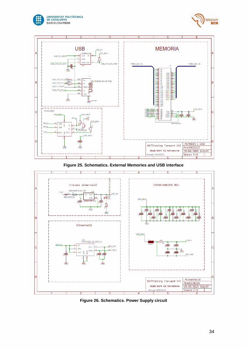
Since image processing require lots of memory resources and processor time a variety of
applications are still using ordinary computers to perform these tasks. Some examples
are video surveillance applications, car license plate number identification, face
recognition applications, etc. Another approach is to use an embedded system for this
kind of applications.
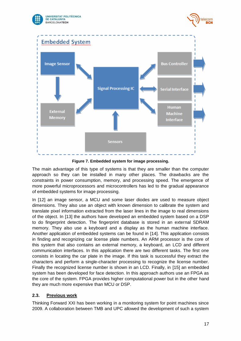
Figure 7 shows a diagram of an embedded system. It consists mainly of an image
sensor, some signal processing Integrated Circuit (IC) like an Application-Specific
Integrated Circuit (ASIC), Digital Signal Processor (DSP), Field Programmable Gate
Array (FPGA), Micro Controller Unit (MCU) or Reduced Instruction Set Computer (RISC)
and optionally some external memory, other sensors, communications IC and interfaces.
The only part of the different approaches that can be changed is the signal processing
unit.
17
Figure 7. Embedded system for image processing.
The main advantage of this type of systems is that they are smaller than the computer
approach so they can be installed in many other places. The drawbacks are the
constraints in power consumption, memory, and processing speed. The emergence of
more powerful microprocessors and microcontrollers has led to the gradual appearance
of embedded systems for image processing.
In [12] an image sensor, a MCU and some laser diodes are used to measure object
dimensions. They also use an object with known dimension to calibrate the system and
translate pixel information extracted from the laser lines in the image to real dimensions
of the object. In [13] the authors have developed an embedded system based on a DSP
to do fingerprint detection. The fingerprint database is stored in an external SDRAM
memory. They also use a keyboard and a display as the human machine interface.
Another application of embedded systems can be found in [14]. This application consists
in finding and recognizing car license plate numbers. An ARM processor is the core of
this system that also contains an external memory, a keyboard, an LCD and different
communication interfaces. In this application there are two different tasks. The first one
consists in locating the car plate in the image. If this task is successful they extract the
characters and perform a single-character processing to recognize the license number.
Finally the recognized license number is shown in an LCD. Finally, in [15] an embedded
system has been developed for face detection. In this approach authors use an FPGA as
the core of the system. FPGA provides higher computational power but in the other hand
they are much more expensive than MCU or DSP.
2.3. Previous work
Thinking Forward XXI has been working in a monitoring system for point machines since
2009. A collaboration between TMB and UPC allowed the development of such a system
18
and the patent [3]. Students involved in the development founded a start-up in order to
implant the system in TMB and in other potential customers.
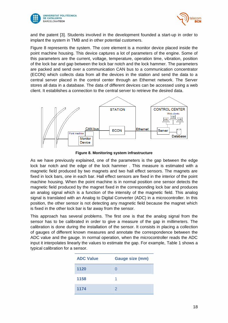
Figure 8 represents the system. The core element is a monitor device placed inside the
point machine housing. This device captures a lot of parameters of the engine. Some of
this parameters are the current, voltage, temperature, operation time, vibration, position
of the lock bar and gap between the lock bar notch and the lock hammer. The parameters
are packed and send over a communication CAN bus to a communication concentrator
(ECON) which collects data from all the devices in the station and send the data to a
central server placed in the control center through an Ethernet network. The Server
stores all data in a database. The data of different devices can be accessed using a web
client. It establishes a connection to the central server to retrieve the desired data.
Figure 8. Monitoring system infrastructure
As we have previously explained, one of the parameters is the gap between the edge
lock bar notch and the edge of the lock hammer . This measure is estimated with a
magnetic field produced by two magnets and two hall effect sensors. The magnets are
fixed in lock bars, one in each bar. Hall effect sensors are fixed in the interior of the point
machine housing. When the point machine is in normal position one sensor detects the
magnetic field produced by the magnet fixed in the corresponding lock bar and produces
an analog signal which is a function of the intensity of the magnetic field. This analog
signal is translated with an Analog to Digital Converter (ADC) in a microcontroller. In this
position, the other sensor is not detecting any magnetic field because the magnet which
is fixed in the other lock bar is far away from the sensor.
This approach has several problems. The first one is that the analog signal from the
sensor has to be calibrated in order to give a measure of the gap in millimeters. The
calibration is done during the installation of the sensor. It consists in placing a collection
of gauges of different known measures and annotate the correspondence between the
ADC value and the gauge. In normal operation, when the microcontroller reads the ADC
input it interpolates linearly the values to estimate the gap. For example, Table 1 shows a
typical calibration for a sensor.
ADC Value Gauge size (mm)
1120 0
1158 1
1174 2
19
1193 3
1205 4
1215 5
Table 1. Example of calibration points
If the ADC gives a measure of 1185 the system estimates the real gap to be 2.58mm as
we can see in the following equation.
The second problem is also related with the calibration. When operators perform the
maintenance tasks on the point machine the calibration process has to be done again.
Usually, maintenance consists in changing some arrangements on the rails and this
changes produce variations in the magnetic field measure. Sometimes maintenance
tasks consists in changing the lock bars. In these cases the magnets have to be fixed
again in new bars and, obviously, the calibration must be done again.
Another problem is that the magnetic sensors are placed in the engine housing and
connected with wires to the monitoring device. Sometimes the wires or the sensors
themselves are broken during maintenance tasks.
Finally there is another issue that affects the actual measure of the gap. The magnetic
field sensor measures the absolute value of the magnetic field in a particular axis. Usually,
lock bars have more than one degree of freedom because of wear by friction. The
movement caused by these additional degrees of freedom introduces errors in measures.
Due to this fact it is possible that the lock bar does not move in the correct direction but in
another one and this produces a variation in the magnetic field that hits the sensor.
In order to solve the above mentioned problems a new device has to be developed. In the
following chapters a device based on an image processing technique will be designed
and developed.
20
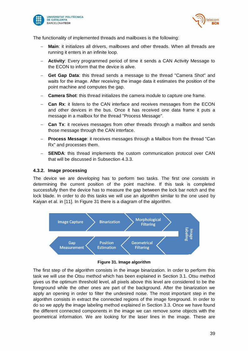
3. Fundamentals
In this chapter we will expose the theory of the methods we are going to use in the image
processing algorithms. We can see a diagram of the proposed algorithm in Figure 31 in
page 39. The first step of the algorithm consists in image binarization. Then, the binary
image is filtered using a morphological filter. Finally the connected regions are found with
a two scan algorithm.
3.1. Optimal threshold in binarization
The first step in most image processing algorithms consists in binarizing the image in
order to extract objects from the background. Image binarization belongs to the group of
the range transform operators. It is a non-reversible operation because it is based on two
clippings.
To binarize an image, we have to clip all the values below a given threshold to 0 and all
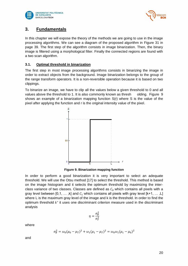
values above the threshold to 1. It is also commonly known as thresh olding. Figure 9
shows an example of a binarization mapping function S(r) where S is the value of the
pixel after applying the function and r is the original intensity value of the pixel.
Figure 9. Binarization mapping function
In order to perform a good binarization it is very important to select an adequate
threshold. We will use the Otsu method [17] to select the threshold. This method is based
on the image histogram and it selects the optimum threshold by maximizing the inter-
class variance of two classes. Classes are defined as which contains all pixels with a
gray level between [0,1, … ,k] and which contains all pixels with gray level [k+1, … ,L]
where L is the maximum gray level of the image and k is the threshold. In order to find the
optimum threshold it uses one discriminant criterion measure used in the discriminant
analysis
where
and
21
is the probability of a pixel to have gray level i and and are the zeroth-order and
first-order cumulative moments of classes defined with kth level. and
are the
between class variance and the total variance of levels respectively. Maximizing the
discriminant criterion η is equivalent to maximizing because
does not depend on
threshold k. Therefore the optimal threshold is found using a sequential search of the
maximum of for all possible values of k=[0, … ,L)
3.2. Mathematical Morphology
In signal processing we use the linear superposition principle. It is based on the unit
impulse and the impulse response which can be computed with the convolution operation.
Figure 10 illustrates the linear superposition principle.
Figure 10. Linear superposition principle
Linear superposition is not good for images as we can see in Figure 11. Applying linear
superposition means that we have to linearly combine different objects in the image. This
is as if the objects were partially transparent. This is not true since objects near the
camera occlude objects in the background.
Figure 11. Linear superposition in images
Mathematical Morphology is used in the field of image processing to analyze images from
the geometrical point of view. It is based on set and lattice theory. Lattice is a
mathematical structure, like the vector space in linear superposition, which is
characterized because it has partial order relation, ≤, and two dual operators, supremum,
, and infimum, .
The infimum of a subset S of a partially ordered set T is the greatest element of T that is
less than or equal to all elements of S. The infimum is also known as the greatest lower
bound. Formally, the infimum of a subset S of a partially ordered set T is an element a of
T such that:
. a is a lower bound, and
22
. a is larger than any other lower bound.
The supremum is the dual concept of infimum. The supremum of a subset S of a partially
ordered set T is the lowest element of T that is more than or equal to all elements of S. It
is also known as the least upper bound. Formally, the supremum of a subset S of a
partially ordered set T is an element a of T such that:
. a is a upper bound, and
. a is smaller than any other upper bound.
One important property of the supremum and infimum is that they are dual. Because of
this, all morphological operators will appear in pair.
Similarly to the unit impulse in the linear space, the point is the basic sequence in the
lattice structure.
Any function in the lattice space can be decomposed using the point. In order to recover
the original function we have to take the supremum at each point.
This allows to define the basic operator in the lattice structure which is the dilation
operator and it is similar to a nonlinear convolution. It is characterized by b[n] which is
called the "structuring element". The dilation is denoted as
The erosion operator is the dual of the dilation. Erosion is similar to a nonlinear
correlation and it is also characterized by the structuring element b[n]. Formally, the
erosion is
In order to compute erosion and dilation in image processing we use a flat structuring
element. This means that the possible values of . Flat structuring element
allows us to perform simple computations, only the min or max of the signal. Furthermore
the output is one of the input samples, this means that the dynamic range of the output is
exactly the same as the dynamic range of the input. Another advantage is that it preserve
the contrast around edges.
The locations where b[n]=0 define a window and the dilation consists in computing the
maximum of gray level values below the window. Dually, the erosion consists in
computing the minimum of gray level values below the window.
Figure 12 shows an example of applying the dilation and erosion operators to a binary
image. For this example, the structuring element is a diamond of size 7x7 pixels with the
23
origin in the center of the structuring element. As we can see in this example the dilation
thickens the objects on the foreground and it removes dark components (min) inside the
foreground objects. In the other hand, erosion flattens the objects in the foreground and
removes bright components (max) in the background. We can observe that both
operators preserve the form of the edges of the image. This represents a great difference
between morphological operators and frequency domain operators.
Figure 12. Erosion and dilation with a diamond structuring element
The combination of dilation and erosion allows us to build new morphological operators.
As we have stated previously, the erosion operation is useful for removing small objects
in the background. However, it has the disadvantage that all the remaining objects shrink
in size as we have seen in Figure 12. This effect can be avoided by applying a dilation
after the erosion with the same structuring element. This combination of operations is
called an opening:
The dual operator of the opening is the closing operator. It consist in concatenating a
dilation with an erosion with the same structuring element:
The main application of the opening consists in removing small objects in the image while
preserving the contours of the objects that remain in the image. The main application of
closing is background simplification. Closing fills small gaps in the objects and gather
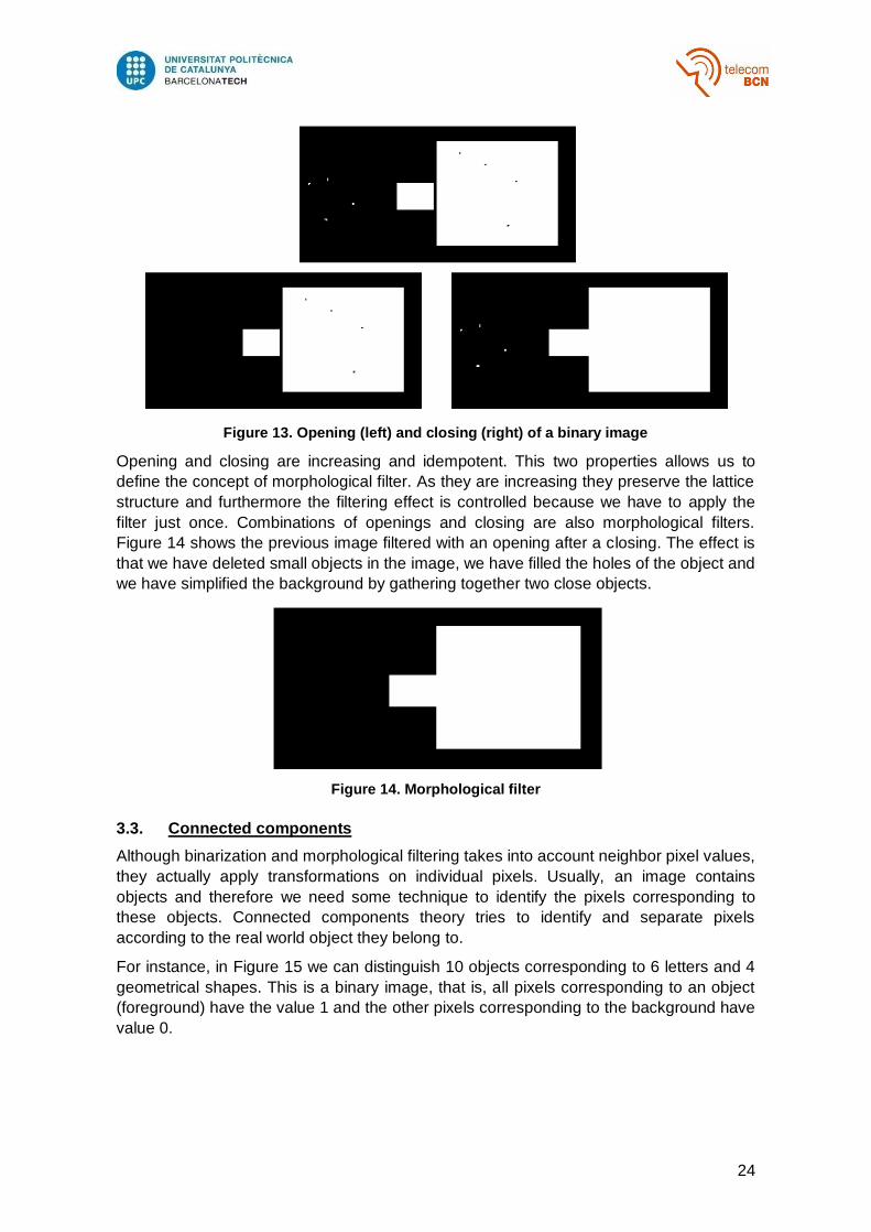
together close objects in the image. Figure 13 illustrates these concepts.
24
Figure 13. Opening (left) and closing (right) of a binary image
Opening and closing are increasing and idempotent. This two properties allows us to
define the concept of morphological filter. As they are increasing they preserve the lattice
structure and furthermore the filtering effect is controlled because we have to apply the
filter just once. Combinations of openings and closing are also morphological filters.
Figure 14 shows the previous image filtered with an opening after a closing. The effect is
that we have deleted small objects in the image, we have filled the holes of the object and
we have simplified the background by gathering together two close objects.
Figure 14. Morphological filter
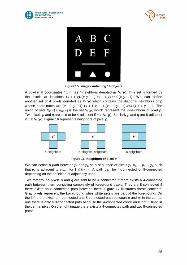
3.3. Connected components
Although binarization and morphological filtering takes into account neighbor pixel values,
they actually apply transformations on individual pixels. Usually, an image contains
objects and therefore we need some technique to identify the pixels corresponding to
these objects. Connected components theory tries to identify and separate pixels
according to the real world object they belong to.
For instance, in Figure 15 we can distinguish 10 objects corresponding to 6 letters and 4
geometrical shapes. This is a binary image, that is, all pixels corresponding to an object
(foreground) have the value 1 and the other pixels corresponding to the background have
value 0.
25
Figure 15. Image containing 10 objects
A pixel p at coordinates has 4-neighbors denoted as . This set is formed by
the pixels at locations We can define
another set of 4 pixels denoted as which contains the diagonal neighbors of p
whose coordinates are . The
union of sets is the set which represent the 8-neighbour of pixel p.
Two pixels p and q are said to be 4-adjacent if . Similarly p and q are 8-adjacent
if . Figure 16 represents neighbors of pixel p.
Figure 16. Neighbors of pixel p
We can define a path between and as a sequence of pixels such
that is adjacent to , for . A path can be 4-connected or 8-connected
depending on the definition of adjacency used.
Two foreground pixels p and q are said to be 4-connected if there exists a 4-connected
path between them consisting completely of foreground pixels. They are 8-connected if
there exists an 8-connected path between them. Figure 17 illustrates these concepts.
Gray pixels represent the background while white pixels are part of the foreground. On
the left there exists a 4-connected and 8-connected path between p and q. In the central
one there is only a 8-connected path because the 4-connected condition is not fulfilled in
the central pixel. On the right image there exists a 4-connected path and two 8-connected
paths.
26
Figure 17. Different types of path between two pixels.
A connected component is the set of all foreground pixels that are connected to each
other, which means that there exists a path between any pair of . Note that
connected component is defined in terms of a path, and the definition of the path
depends on adjacency, therefore we need to define the type of adjacency to find the
connected components of an image.
27
4. Methodology / project development
In this chapter we will explain the key aspects of the design. We will start by establishing
the system specifications that fulfill the goals presented in Section 1.3. Then we will
continue explaining the hardware design which involves not also the electronics but the
optical element and the housing of the device. After that, a communication challenge will
be presented and we will explain a custom communication protocol to solve it. Finally the
image processing algorithms will be discussed.
4.1. System specifications
The device must be designed taking into account the goals stated in Section 1.3 and the
size constraints.
First of all the device must be easy to install. There are only 3 daily hours to
perform the maintenance tasks and maintenance teams are small according to
the size of the infrastructure to maintain. The easier to install the device the better.
This should be taken into account in the hardware, especially in the box design,
and in the firmware design.
The device needs to be robust in two senses. The first is directly related to the
hardware design because it has to be installed inside a point machine which is
subject to vibration, temperature changes, dust and humidity. The box of the
device must resist this unfavorable conditions. The other sense refers to the
repeatability and confidence of the measurements and it is related with the
software design and implementation. The error rate of the device should be less
than 5%, including bad measures and unknown measures when the lock bar is in
its correct position.
The minimum total gap to measure is of 5 millimeters. Maintenance operators
want to know where the gap is less than 10% in order to plan a task to correct the
position of the bars. The precision of the measurement should be less than
0.5mm and it is desirable to be 0.25mm. This should be taken into account to
determine the resolution of the CCD and image processing algorithms.
Another constraint of the system is the execution time that consists in the image
capture plus the image processing times. The image capture time is determined
by the hardware (the image sensor, the microcontroller and the memory latency).
The image algorithm determines the processing time. As it has been explained in
Section 1.3 the device has two modes of operation. In normal operation it gives a
measure every 10 seconds. In general, the execution time could be up to 10
seconds. In continuous operation the device must provide at least one measure
per second. This has to be considered in the design of the image processing
algorithm.
Power consumption has also been taken into account. The wire length between
the control cabin and the point machine location can sometimes be quite long, up
to 1Km. The device is powered by a DC voltage up to 24V with a cable of 1.5mm2.
The resistivity of the copper is
28
as we can see in [16]. S is the section of the conductor in squared meters and l is
the wire length in meters. We can compute the total wire resistance as
If we take, for instance, that the device consumes 150mA, the total drop of
potential at the device is
Typically the same cable is used to power more than one device so the power
consumption represents a constraint on the design. This constraint relates not
only with the hardware but also with the firmware of the device. If the execution
time is so long that the device is always running then the power consumption
increases and it probably does not fulfill the power consumption constraint.
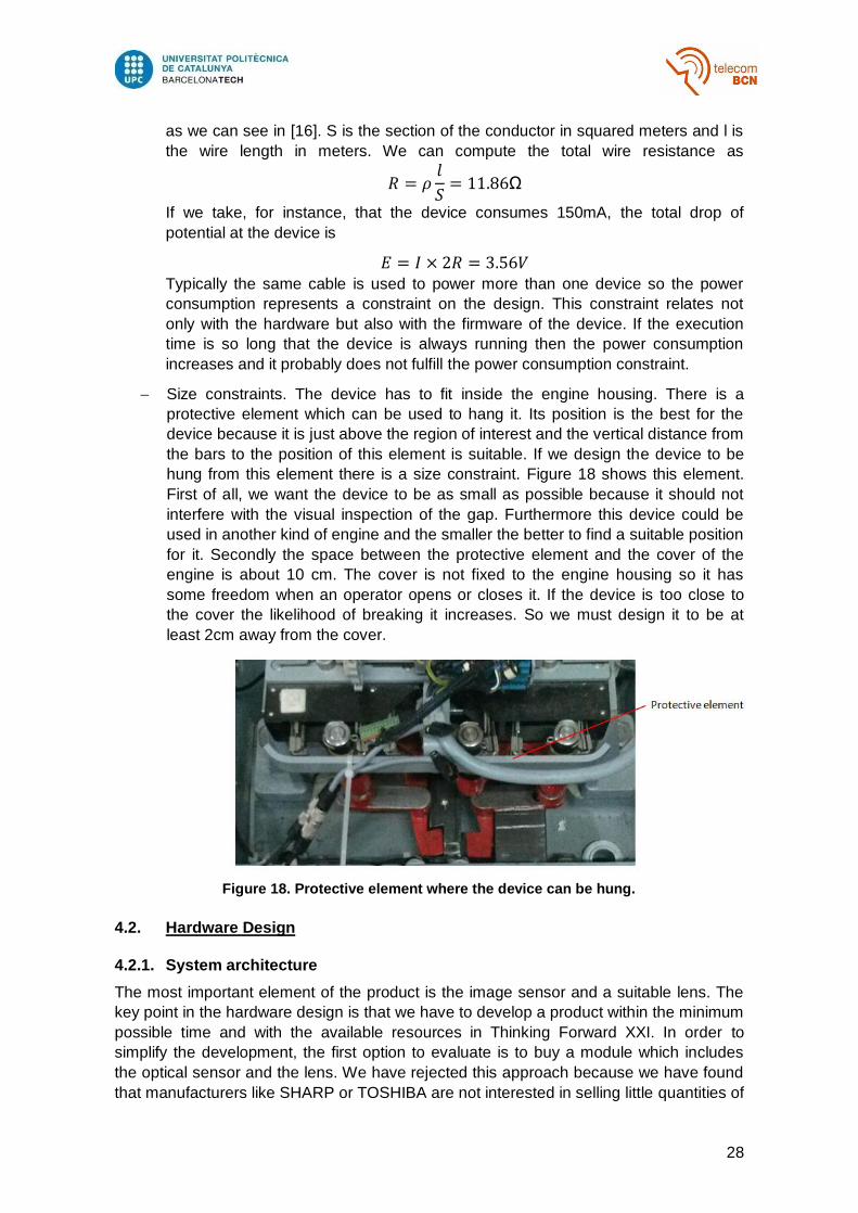
Size constraints. The device has to fit inside the engine housing. There is a
protective element which can be used to hang it. Its position is the best for the
device because it is just above the region of interest and the vertical distance from
the bars to the position of this element is suitable. If we design the device to be
hung from this element there is a size constraint. Figure 18 shows this element.
First of all, we want the device to be as small as possible because it should not
interfere with the visual inspection of the gap. Furthermore this device could be
used in another kind of engine and the smaller the better to find a suitable position
for it. Secondly the space between the protective element and the cover of the
engine is about 10 cm. The cover is not fixed to the engine housing so it has
some freedom when an operator opens or closes it. If the device is too close to
the cover the likelihood of breaking it increases. So we must design it to be at
least 2cm away from the cover.
Figure 18. Protective element where the device can be hung.
4.2. Hardware Design
4.2.1. System architecture
The most important element of the product is the image sensor and a suitable lens. The
key point in the hardware design is that we have to develop a product within the minimum
possible time and with the available resources in Thinking Forward XXI. In order to
simplify the development, the first option to evaluate is to buy a module which includes
the optical sensor and the lens. We have rejected this approach because we have found
that manufacturers like SHARP or TOSHIBA are not interested in selling little quantities of
29
their integrated modules and furthermore almost all available modules in the market have
a CCTV output that it is not useful for our application.
The second option we have evaluated is to use an image sensor with a microcontroller.
There are some reasons why we are going to develop this device using this option. First
of all, the team in Thinking Forward XXI which is going to design and develop the device
has some expertise in developing hardware based on microcontrollers. Secondly,
microcontrollers are cheaper than FPGA or ASICs. And finally we have a first prototype
designed with this approach. In addition, the microcontroller approach has been used by
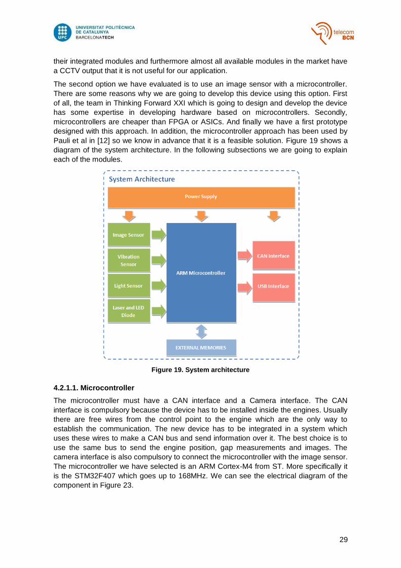
Pauli et al in [12] so we know in advance that it is a feasible solution. Figure 19 shows a
diagram of the system architecture. In the following subsections we are going to explain
each of the modules.
Figure 19. System architecture
4.2.1.1. Microcontroller
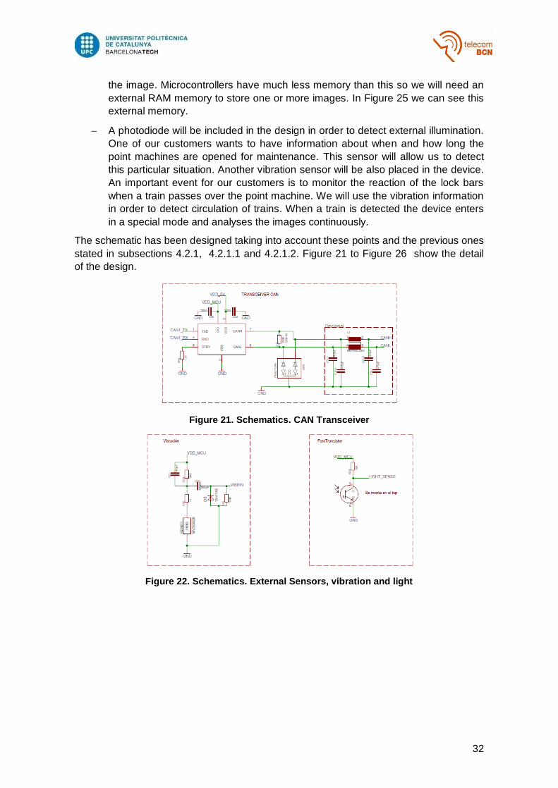
The microcontroller must have a CAN interface and a Camera interface. The CAN
interface is compulsory because the device has to be installed inside the engines. Usually
there are free wires from the control point to the engine which are the only way to
establish the communication. The new device has to be integrated in a system which
uses these wires to make a CAN bus and send information over it. The best choice is to
use the same bus to send the engine position, gap measurements and images. The
camera interface is also compulsory to connect the microcontroller with the image sensor.
The microcontroller we have selected is an ARM Cortex-M4 from ST. More specifically it
is the STM32F407 which goes up to 168MHz. We can see the electrical diagram of the
component in Figure 23.
30
4.2.1.2. Image Sensor
In order to select the image sensor we have to take into account the resolution we want
to achieve. The area we have to analyze is more or less a square of side w=12cm side.
The resolution we want to achieve is about 0.25mm as we have said in Section 4.1. We
can compute the minimum resolution of the sensor in pixels to be
Nor the maximum resolution neither the number of channels are important parameters for
this application. Although the maximum resolution should be taken into account because
it is related to the processing time, it is not a restrictive parameter in this application
because usually image sensors can be configured to the desired resolution. Despite the
application only requires one channel images (gray level images), color sensors have the
same price as gray sensors.
Another important aspect to take into account is the availability of the sensor. After talking
with some sensor manufacturers and distributors we have found that the best choice is
Aptina. Although you have to sign a non disclosure agreement (NDA), the sensors can be
bought in any component provider like RS or Farnell. After signing the NDA Aptina
provides useful datasheets and developer guides that allows you to configure the sensor.
Taking this into account we have requested information about an Aptina and an
Omnivision sensor and finally we have selected the MT9M131C12STC sensor from
Aptina because the documentation is much better. It is a 1.3Mpx color sensor and it can
be configured through an I2C interface which is also available in the selected
microcontroller. In Figure 24 we can see the electrical diagram of the device and the
signals connected to it.
4.2.1.3. Light Pattern
In Section 4.3.2.5 and 4.3.2.6 we will explain how we estimate the position and compute
the gap. The solution with a better performance and that allows us to reduce the
processing time is to use some kind of structured light.
We have considered using a single laser with a Diffractive Optical Element (DOE). DOE's
allows to control the beam's shape of the laser light allowing us to have different patterns
with the same laser component.
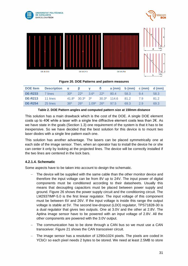
We have tested 3 different DOE elements whose patterns can be found in Figure 20. In
this figure we can also see the measures of the patterns produced by the elements. In
Table 2 we can find the pattern angles for each element.
The DOE have to be placed, approximately, at 150mm of the plane we have to measure.
The computed size of the projected pattern at this distance can be also found in Table 2.
To compute the pattern size we have applied the following trigonometric relation
considering that the laser beam goes from a single dot to the interest plane following a
straight line.
The same computation has been applied to the other measures b, c and d. The region of
interest is about d=60mm and b=80mm. Taking into account this measures the DOE
which fits better for our application is the 11 lines one.
31
Figure 20. DOE Patterns and pattern measures
DOE Item Description α β γ δ a (mm) b (mm) c (mm) d (mm)
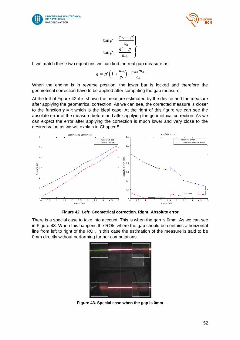
There is a special case to take into account. This is when the gap is 0mm. As we can see
in Figure 43. When this happens the ROIs where the gap should be contains a horizontal
line from left to right of the ROI. In this case the estimation of the measure is said to be
0mm directly without performing further computations.
Figure 43. Special case when the gap is 0mm
53
4.3.3. Custom communication protocol over CAN
The device we are developing has to be placed inside the point machine engine housing.
Furthermore it has to be integrated in the current monitoring system explained in Section
2.3. The easiest way to integrate the new device into the system is using the same
communication bus to transfer the computed data and the captured images when
necessary. This bus is a two pair CAN bus. The CAN specification can be found in [18].
The most important points are that a CAN data frame can have up to 8 bytes and CAN
specification does not provide neither reliable nor ordered delivery of data frames.
The transmission of the point machine position estimation and the gap measurement can
be done within one single data frame so it does not require any special protocol. A simple
ACK mechanism is used to ensure that the data arrives to its destination.
On the other hand, one data frame it is not enough to send the entire image to the server.
We must send a large number of CAN frames. We cannot send an ACK for every single
data frame so we must implement a custom protocol over the CAN layer to ensure that all
the image bytes arrive to their destination.
The custom protocol must ensure that all frames arrive to the communications
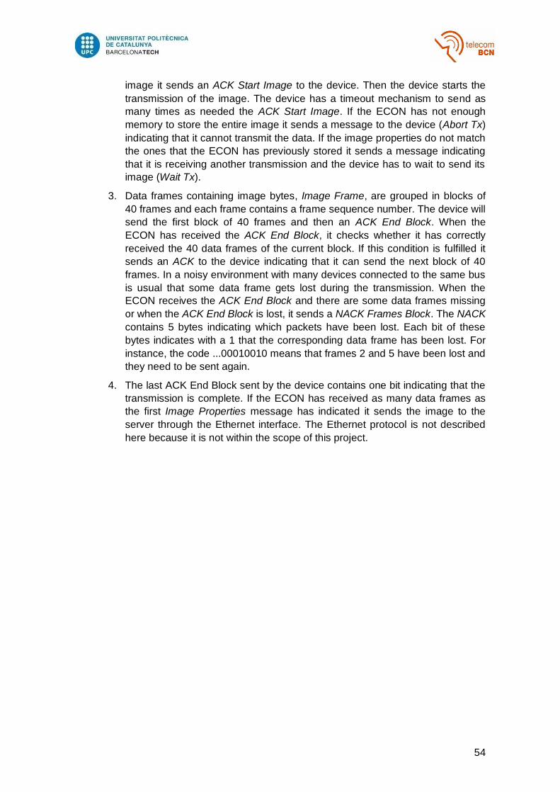
concentration device and that they arrive in the right order. Figure 45 in page 56 shows
the diagram of this protocol. The key aspects of the protocol are the following:
The transmission has an identification number. Every data frame corresponding to
the same transmission contains one byte with this identification number.
The first frame of the protocol contains the number of bytes that will be sent.
Each data frame with image data bytes contains a sequence number indicating
the position of the data.
ACK is used in order to ensure that all frames arrive to the receiver.
NACK is sent to the transmitter to say that some frames have been lost. The
transmitter must send again the lost frames.
4.3.3.1. Protocol description
Figure 44 shows the structure of the data frames with the information that each one
contains. The protocol, which can be seen in Figure 45, is as follows.
1. The protocol can start by two different ways:
a. Some device in the system sends a message (Send Data Request)
indicating to the device that it has to send an image. In this case, the
device sends a message indicating that it has received the request and
will take and send the image (Wait Data). Then the device takes a
picture, performs the corresponding computations and it sends the
data and/or the image.
b. The device has detected an abnormal situation and it decides to send
the image.
2. In both cases, when the device has an image ready to send to the server, it
sends a data transfer request (Image Properties) to the communication
concentration device (ECON). In the data transfer request there is information
about the type and length of the data. When the ECON is ready to receive the
54
image it sends an ACK Start Image to the device. Then the device starts the
transmission of the image. The device has a timeout mechanism to send as
many times as needed the ACK Start Image. If the ECON has not enough
memory to store the entire image it sends a message to the device (Abort Tx)
indicating that it cannot transmit the data. If the image properties do not match
the ones that the ECON has previously stored it sends a message indicating
that it is receiving another transmission and the device has to wait to send its
image (Wait Tx).
3. Data frames containing image bytes, Image Frame, are grouped in blocks of
40 frames and each frame contains a frame sequence number. The device will
send the first block of 40 frames and then an ACK End Block. When the
ECON has received the ACK End Block, it checks whether it has correctly
received the 40 data frames of the current block. If this condition is fulfilled it
sends an ACK to the device indicating that it can send the next block of 40
frames. In a noisy environment with many devices connected to the same bus
is usual that some data frame gets lost during the transmission. When the
ECON receives the ACK End Block and there are some data frames missing
or when the ACK End Block is lost, it sends a NACK Frames Block. The NACK
contains 5 bytes indicating which packets have been lost. Each bit of these
bytes indicates with a 1 that the corresponding data frame has been lost. For
instance, the code ...00010010 means that frames 2 and 5 have been lost and
they need to be sent again.
4. The last ACK End Block sent by the device contains one bit indicating that the
transmission is complete. If the ECON has received as many data frames as
the first Image Properties message has indicated it sends the image to the
server through the Ethernet interface. The Ethernet protocol is not described
here because it is not within the scope of this project.
55
Figure 44. Image Transmission data frames
56
Figure 45. Custom communication protocol diagram
57
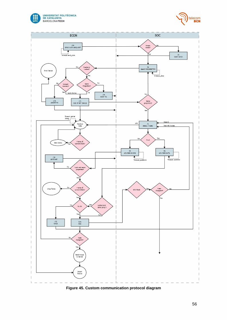
4.3.4. Installation Program
A desktop program has been developed to configure the device during its installation.
The program allows the operator to configure the following information:
Position of the ROIs: The ROIs have to be placed at the edges of the lock
hammers.
Angle of the hammer in normal and reverse position: The angle of the lock
hammer edge have to be configured. It is configured by clicking in a point of the
edge and moving the cursor towards the edge. A line is displayed to help the
operator to configure this angle.
Power of lasers: This is configured from 1% to 100%. This control is needed
because the reflection of the light is different in every point machine. Furthermore
we have realized that the reflection of the lasers is very different in both parts of
the lock hammer. This is due to the position of the lasers. The device is just above
the right edge of the hammer and the reflection of the laser in the vertical is higher
than in the right edge of the image. We have created a control to configure two
different powers for the laser and the camera takes two shots. In the first shot it
captures the right part of the image up to the middle of the ROIs and in the
second one it captures the rest of the image. The device combines these two
shots to build a single image as we can see in Figure 46.
Manual exposition: It allows to configure the exposition value of the image sensor.
Maximum gap value: Some point machines have the maximum gap value bigger
than the standard of 5mm.
Take picture: The device takes a picture, computes the gap, draws the
augmented reality and sends the image through the USB port to the PC. It is also
possible to take the picture without the augmented reality or taking only the
minimum window which contains the four ROIs.
Figure 46. Installation Program
58
4.3.5. Web Client Integration
All information is collected by a central server and stored in a database. Final clients can
access data using a web client. The web client is a dashboard based application. We
developed such an application because it is customizable by every user. There is a home
dashboard which each user can configure with different widgets according to its specific
role in the organization.
In the home dashboard there is general information about the whole system. When a
user wants to analyze a specific point machine, he or she can access to the dashboard of
the point machine. This dashboard, showed in Figure 47, displays specific information
about the point machine. The point machine position, the gap measurement and images
from the device will be displayed in some widgets of this dashboard.
In the point machine dashboard we can find real time information that is updated every
second like the widget with the lock bar and lock hammer diagram in the right of the
dashboard. Below this widget there is another real time widget that displays the position
of the point machine, number of operations, temperature and the current gap. Data from
the developed device has been added to these two widgets. In the first one, the lock bar
moves from right to left indicating the current gap. When the gap is below a configured
threshold, for instance 0.5mm, the diagram is displayed in red indicating that the position
of the lock bar is not appropriate. In the second widget the measure is also displayed as
text.
At the side of these widgets there is another one that displays the data collected after an
operation. In this widget we find information about operation time, current consumption,
voltage, power, vibration... The gap measurement just after the operation has also been
added to this widget.
Finally we have developed a widget that contains an image gallery with all images taken
by the device in this specific point machine. At the bottom of the image we have added
the date and time where the image was received by the central server and the detected
position. We have added controls to this widget to navigate through images and to take a
new picture. When a user presses the 'Take Picture' button a message is sent to the
device which captures a new image, computes the gap and sends the data and the
image to the server. The image is automatically updated when it has been completely
received. The process of taking an image and sending it over the network to the central
server takes about 30 seconds.
59
Figure 47. Dashboard of a point machine.
60
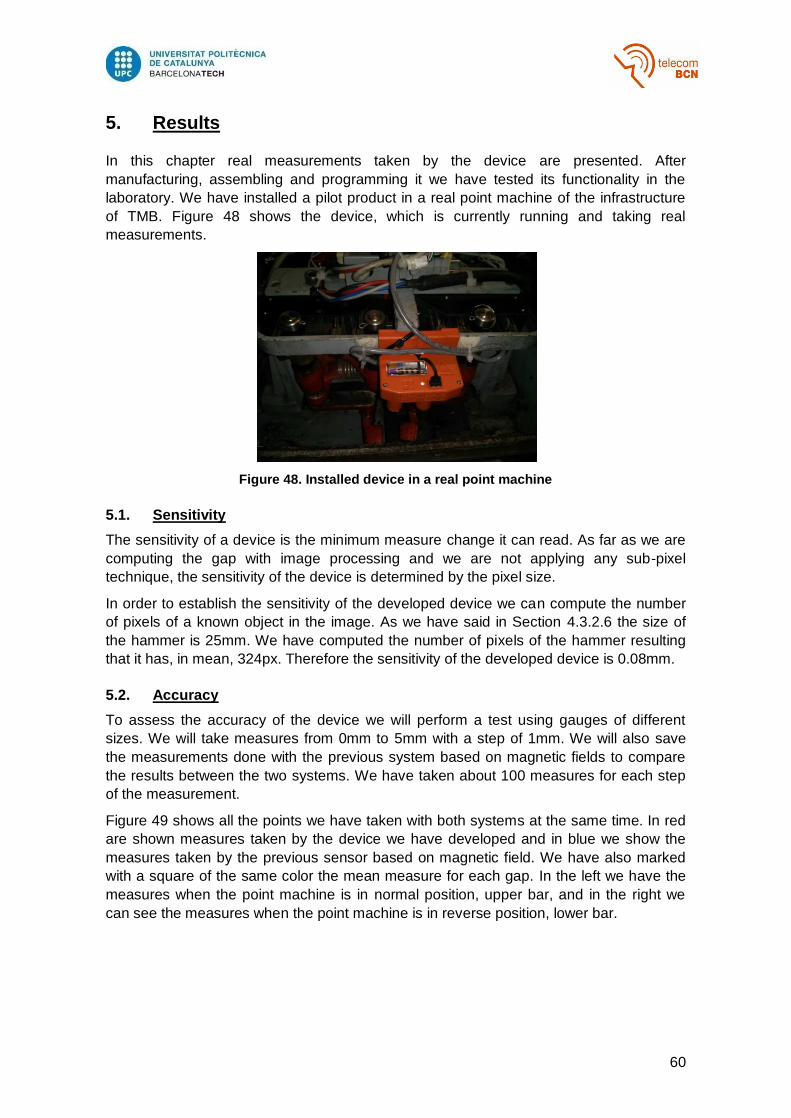
5. Results
In this chapter real measurements taken by the device are presented. After
manufacturing, assembling and programming it we have tested its functionality in the
laboratory. We have installed a pilot product in a real point machine of the infrastructure
of TMB. Figure 48 shows the device, which is currently running and taking real
measurements.
Figure 48. Installed device in a real point machine
5.1. Sensitivity
The sensitivity of a device is the minimum measure change it can read. As far as we are
computing the gap with image processing and we are not applying any sub-pixel
technique, the sensitivity of the device is determined by the pixel size.
In order to establish the sensitivity of the developed device we can compute the number
of pixels of a known object in the image. As we have said in Section 4.3.2.6 the size of
the hammer is 25mm. We have computed the number of pixels of the hammer resulting
that it has, in mean, 324px. Therefore the sensitivity of the developed device is 0.08mm.
5.2. Accuracy
To assess the accuracy of the device we will perform a test using gauges of different
sizes. We will take measures from 0mm to 5mm with a step of 1mm. We will also save
the measurements done with the previous system based on magnetic fields to compare
the results between the two systems. We have taken about 100 measures for each step
of the measurement.
Figure 49 shows all the points we have taken with both systems at the same time. In red
are shown measures taken by the device we have developed and in blue we show the
measures taken by the previous sensor based on magnetic field. We have also marked
with a square of the same color the mean measure for each gap. In the left we have the
measures when the point machine is in normal position, upper bar, and in the right we
can see the measures when the point machine is in reverse position, lower bar.
61
Figure 49. Measures and mean
As we can see in the previous figure, the results are quite good but we need to perform
some measures to assess its actual quality. We take the gauge size as the real gap. It is
important to note that sometimes it is very difficult to put the gap exactly as the gauge
size because when it is taken away it produces a small undesired movement of the lock
bar.
We compute the absolute error for each measure as:
where is the measure of the gap and is the size of the gauge we have used to take
the measure. Figure 50 shows measurement errors for the developed device and the
magnetic field sensor.
Figure 50. Absolute error
In general, absolute error tends to be bigger when the real measure is high. It is for this
reason that relative error, usually, is more useful than absolute error. Despite of this, it
seems that for devices under study this effect is not relevant. This is because the error is
constant all over the range of the measure. In the case of the image sensor, the error is
always produced by one or, at most, two pixels. The pixel size remains always constant
62
because the device is fixed in its position so the error is the same when measuring small
gap and large gaps.
The error when the gap is 0mm is a special case because the estimation of the gap is
different as we have seen at the end of Section 4.3.2.6. Another special case is when the
real gap is 5mm. As far as we know that the maximum gap is 5mm, because it is
configured during the installation process, when a measure is higher than this value the
device crops it to 5mm.
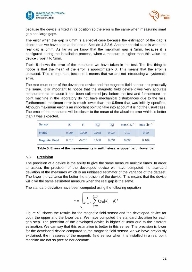
Table 5 shows the error of the measures we have taken in the test. The first thing to
notice is that the mean of the error is approximately 0. This means that the error is
unbiased. This is important because it means that we are not introducing a systematic
error.
The maximum error of the developed device and the magnetic field sensor are practically
the same. It is important to notice that the magnetic field device gives very accurate
measurements because it has been calibrated just before the test and furthermore the
point machine in the laboratory do not have mechanical disturbances due to the rails.
Furthermore, maximum error is much lower than the 0.5mm that was initially specified.
Although maximum error is an important point to take into account it is not the usual case.
The error of the measures will be closer to the mean of the absolute error which is better
than it was expected.
Sensor
Image 0.004 0.009 0.038 0.034 0.10 0.10
Magnetic Field 0.013 -0.016 0.068 0.031 0.098 0.109
Table 5. Errors of the measurements in millimeters. u=upper bar, l=lower bar
5.3. Precision
The precision of a device is the ability to give the same measure multiple times. In order
to assess the precision of the developed device we have computed the standard
deviation of the measures which is an unbiased estimator of the variance of the dataset.
The lower the variance the better the precision of the device. This means that the device
will give the same estimated measure when the real gap is the same.
The standard deviation have been computed using the following equation
Figure 51 shows the results for the magnetic field sensor and the developed device for
both, the upper and the lower bars. We have computed the standard deviation for each
gap step. The precision of the developed device is higher at 0mm due to the different
estimation. We can say that this estimation is better in this sense. The precision is lower
for the developed device compared to the magnetic field sensor. As we have previously
explained, the measures of the magnetic field sensor when it is installed in a real point
machine are not so precise nor accurate.
63
Figure 51. Standard deviation of the measures
Finally we have computed the standard deviation of all measures. To perform this
computation we have taken into account that the mean value is different for every gap
step of the dataset. So we have divided the dataset in subsets according to the real gap
and computed the mean value for every subset. We have used these means to subtract
them from the measure in standard deviation equation. Results are presented in Table 6.
For the upper bar the standard deviation is 0.0232mm, this means that with a probability
of 99.7% the measure will be in the range ±0.0696mm. For the lower bar we have a
worse result, the 99.7% of the measures will be in the rage ±0.2088mm.
Sensor
Image 0.0232 0.0502
Magnetic Field 0.0093 0.0101
Table 6. Standard deviation
In general, results for the lower bar are slightly worse than results for the upper bar. This is probably due to the geometrical correction that we apply to this measure as we have explained in Section 4.3.2.6. To compute this correction we use the position of the device relative to the lock hammer. Small errors in the position determination are propagated to the final gap measure.
64
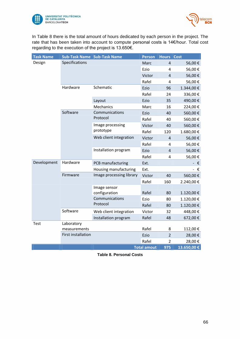
6. Budget
In this chapter we present the total amount in materials and personal costs of the project.
One specification for the device is that it has to be inexpensive. We present here this
information in order to check whether this specification is fulfilled or not.
In Table 7 we can see the Bill of materials (BOM) for one prototype. We have also
computed the cost of manufacturing the PCB and mounting it. We have added this in the