Page 1
The Microelectronics Training Center, IMEC v.z.w.www.imec.be/mtc
delfi.imec.be
MTC 2008 : Prospects and Challenges of Redox-based RRAM ConceptsIMEC© 2008
Rainer WaserPage 1
Rainer WaserJülich-Aachen Research Alliance JARA,
Section Fundamentals of Future Information TechnologyFZJ Jülich & RWTH Aachen University
Outline1 Introduction2 Electrochemical metallization effect
- cation migration redox systems3 Valence change switching effect
– anion migration redox systems4 Thermochemical switching effect5 Conclusion
1. 행사 기본 개요IMST Tutorial 2008
Prospects and Challenges of Redox-based RRAM Concepts
Resistive Switching Group * Kristof Szot
* Regine Dittmann* K. Shibuya (Humboldt fellow)
* Tobias Menke
Acknowledgement* S. Blügel, G. Bihlmeyer, K. Urban, C. L. Jia
(JARA-FIT & IFF, FZ Jülich)* Stan Williams et al. (HP labs)* Hasegawa (Aono group)* R. Bruchhaus, M. Kund (Qimonda)* M. Kozicki (ASU)
* HGF, DFG * bmbf, Qimonda, EU EMMA, Intel Corp.
Funding
* Christine Schindler (now Siemens)
* Ruth Münstermann
- 2
* Shen Wan
* Carsten Kügeler (head of the NAL)
* Herbert Schroeder
Page 2
The Microelectronics Training Center, IMEC v.z.w.www.imec.be/mtc
delfi.imec.be
MTC 2008 : Prospects and Challenges of Redox-based RRAM ConceptsIMEC© 2008
Rainer WaserPage 2
- 3
• often an initial electrical formation (defined stress) needed• „write“-Operation by large voltage pulses
(typically with current compliance) • „read“ operation by small (sensing) voltage pulses
Operation Electrical switching between ON(LRS) and OFF(HRS) state
Polarity modes of RRAM
I
V
Read
RESET
RESET
SET
SET
I
V
Read
RESET
SET
Unipolar (symmetrical) - URS Bipolar (antisymmetrical) - BRS
Basic Definitions of Resistive RAM
History • many reports since the 1960s • mainly binary oxides, mainly unipolar switching• Stan Williams et al. (2008):
memristor / memristive devices according to L. Chua
CC
CC
CC
Page 3
The Microelectronics Training Center, IMEC v.z.w.www.imec.be/mtc
delfi.imec.be
MTC 2008 : Prospects and Challenges of Redox-based RRAM ConceptsIMEC© 2008
Rainer WaserPage 3
Resistive SwitchingMemories
MolecularC
onfi-guration
Mem
ory
Electrostatic/ FE
Effects
Phase Change
Mem
ory
Thermochem
icalEffect
ValencyC
hangeEffect
Electrochemical
metallization
cell
Magnetoresistive
Mem
oryEffects
Ferroelectric/ M
F Tunneling
Emerging Memories: Classification of the mechanisms
Nanom
echanicalM
emory
Redox-basedswitching
phenomenain chalcogenides
Resistive SwitchingMemories
Electrostatic/ FE
Effects
Phase Change
Mem
ory
Thermochem
icalEffect
ValencyC
hangeEffect
Electrochemical
metallization
cell
Magnetoresistive
Mem
oryEffects
Ferroelectric/ M
F Tunneling
Emerging Memories: Classification of the mechanisms
Nanom
echanicalM
emory
MolecularC
onfi-guration
Mem
ory
Page 4
The Microelectronics Training Center, IMEC v.z.w.www.imec.be/mtc
delfi.imec.be
MTC 2008 : Prospects and Challenges of Redox-based RRAM ConceptsIMEC© 2008
Rainer WaserPage 4
Confinement of the Switching Event
Important issue
• homogeneouslydistributed effect?
Location of the switching event - In the electrode area
• effect confined to filaments?
Waser & Aono, Nat.Mat. (2007) A. Sawa, Mat.Today (2008)
- 8
Page 5
The Microelectronics Training Center, IMEC v.z.w.www.imec.be/mtc
delfi.imec.be
MTC 2008 : Prospects and Challenges of Redox-based RRAM ConceptsIMEC© 2008
Rainer WaserPage 5
Electrochemical Metallization Memory
OperationON-switching:Reduction @ cathode→ Ag filament formation
Ag+ + e‘ → Ag
OFF-switching:Oxidation @ anode
Ag → Ag+ + e‘ or
M. Faraday (1834)
Names: ElectrochemicalMetallization Memory (ECM); PMC; CBRAM
Electrolyte* amorphous GeSe2+x and GeS2+x* Disordered and amorphous
sulfides and oxides
Ag/GeSex
Qimonda group (2006)
Hirose & Hirose(1976)
+10 μA
-10 μA
Aono et al (2005)
-1 0 +1 V
Kozicki (1997)
SiO2 – an unconventional ECM electrolyte
States and ProcessesLooking at the elementary steps
C. Schindler et al. (2007)
Pt
Cu Cu
Cu
Pt
Pt
SiO2 SiO2
SiO2
Page 6
The Microelectronics Training Center, IMEC v.z.w.www.imec.be/mtc
delfi.imec.be
MTC 2008 : Prospects and Challenges of Redox-based RRAM ConceptsIMEC© 2008
Rainer WaserPage 6
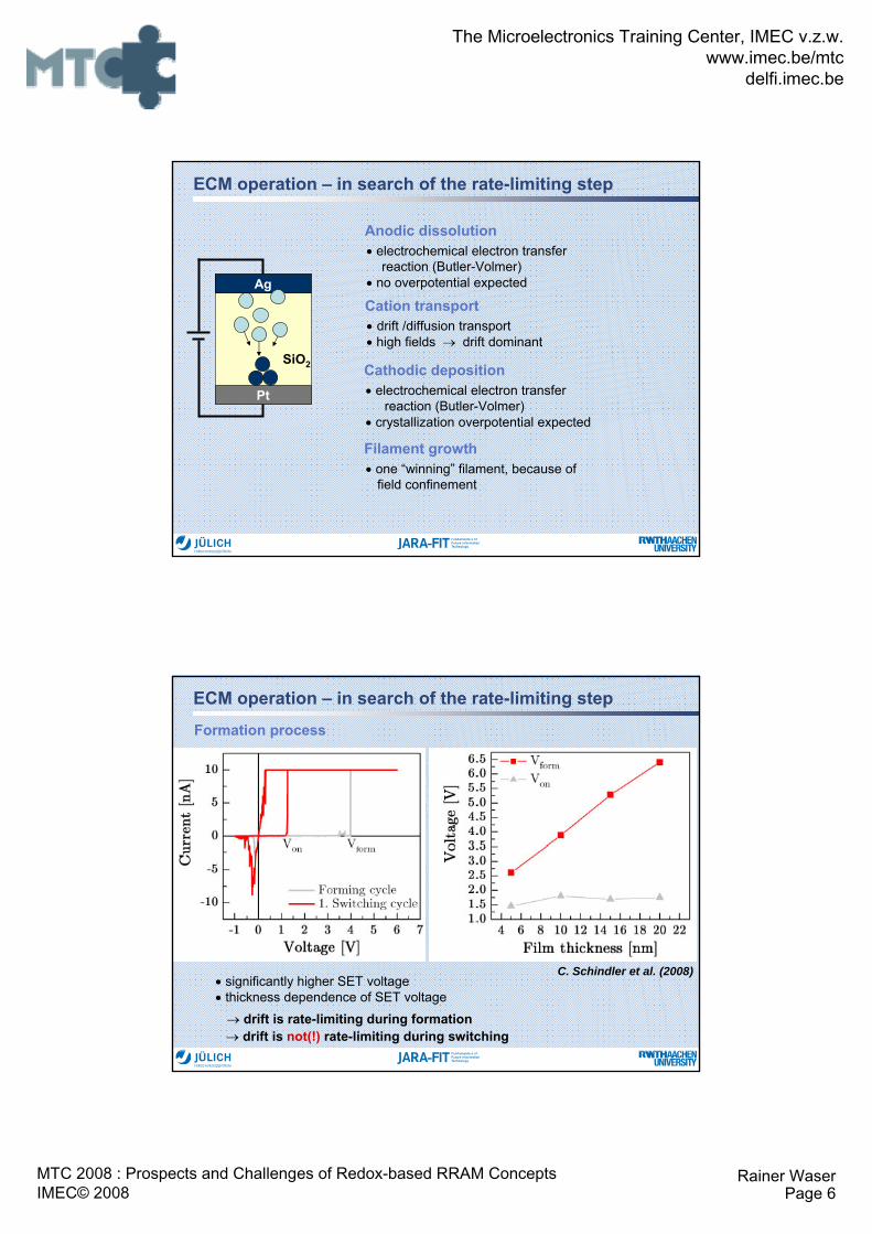
ECM operation – in search of the rate-limiting step
Anodic dissolution• electrochemical electron transfer
reaction (Butler-Volmer)• no overpotential expectedAg
Pt
Cation transport• drift /diffusion transport• high fields → drift dominant
SiO2 Cathodic deposition• electrochemical electron transfer
reaction (Butler-Volmer)• crystallization overpotential expected
Filament growth• one “winning” filament, because of
field confinement
ECM operation – in search of the rate-limiting step
Formation process
• significantly higher SET voltage• thickness dependence of SET voltage→ drift is rate-limiting during formation→ drift is not(!) rate-limiting during switching
C. Schindler et al. (2008)
Page 7
The Microelectronics Training Center, IMEC v.z.w.www.imec.be/mtc
delfi.imec.be
MTC 2008 : Prospects and Challenges of Redox-based RRAM ConceptsIMEC© 2008
Rainer WaserPage 7
ECM operation – in search of the rate-limiting step
Kinetics of the SET process
• SET voltage Von depends exponentially on 1/ramp rate(over > 8 orders of magnitude!!)
• a threshold voltage exists
→ RRAM application:guarantees fast switching andlong retention times
→ Understandingprocess is cationic electrontransfer reaction limited!
C. Schindler et al. (2008)
for Cu / SiO2(15nm) / Ir cells
ECM operation – in search of the rate-limiting step
Kinetics of the cathodic reaction
1. possibility: Electron transfer Butler-Volmer-equatione-
⎥⎦
⎤⎢⎣
⎡⎟⎠⎞
⎜⎝⎛ −−−⎟
⎠⎞
⎜⎝⎛=
kTze
kTzeii ηαηα )1(expexp 0
0( )( , ) exp c
cN zei K Z N
kTα η+⎡ ⎤= ⎢ ⎥⎣ ⎦
2. possibility: nucleation overpotential
Z0: areal density of nucleation sites
Nc: number of atoms of a critical nucleus
C. Schindler et al. (submitted)
Page 8
The Microelectronics Training Center, IMEC v.z.w.www.imec.be/mtc
delfi.imec.be
MTC 2008 : Prospects and Challenges of Redox-based RRAM ConceptsIMEC© 2008
Rainer WaserPage 8
( ) ( ) ( ) ( )+ Δ = + Δ + Δ + Δ2i i 1 2
Compute location G
i i i
x
x t t x t c t v t c t a t x
( )= ≠
+ Δ = − − ∑1,
compute forces on ions2 N
plate Coulombi
Cu Cuj i j
eE Fa t tm m
( )( )
( )
=
= = Δ
= = −
0 distributed uniformly
02
0
iG
i i
platei
Cu
x t
v t veE
a tm
iCompute velocity v
ion docked ?
dendrite complete ?Finish
= + Δt t t
= + Δt t t
drop new ion
No
No
Yes
Yeselectrode rct(Butler-Volmer)
40 nm
ECM – Molecular Dynamics Modeling
S. Menzel, R. Waser, to be published
Growth speed of a (cylindrical) nanofilament
A2
A 0
[cm/s] [A]Mh Ir zN eπ ρ
=&
Example: Ag filament of 10nm diameterat I = 1 μA
1.3m/sh→ &
Location of the RESET eventAfter SET metal filament (e.g. Ag)RESET where will the filament will open ?
Experimental / theoretical finding: at Ag filament / Ag electrode contact
General questionSituation after RESET – chemically symmetrical cell ! How can a symmetrical cell switch in a bipolar fashion?Possible answer Morphological effect (?)
Impact on long-term reliability (?)
RESETb) late ON-statec) Early OFF-StateV = 200mV(steps 10 mV)
X. Guo, C. Schindler,S. Menzel, R. Waser, APL (2007)
- 16
ECM operation – RESET issue Ag
Pt
Page 9
The Microelectronics Training Center, IMEC v.z.w.www.imec.be/mtc
delfi.imec.be
MTC 2008 : Prospects and Challenges of Redox-based RRAM ConceptsIMEC© 2008
Rainer WaserPage 9
- 17
Capacitor-like structure with Cr-doped SrZrO3 thin films PCMO thin films (Ba,Sr)TiO3 thin films TiO2 thin films SrTiO3 Single crystalsas resistive element
A. Beck, J. G. Bednorz, Ch. Gerber, C. Rossel and D. Widmer, Appl. Phys. Lett. 77, 139 (2000).
SrZrO3(0.2 %Cr)
SrTiO3 (100)
Pt
SrRuO3
300 nm
Examples
after forming process: reversible bipolar switching between stableimpedance states
- 18
Bipolar resistive switching in transition metal oxides
Characteristics
Page 10
The Microelectronics Training Center, IMEC v.z.w.www.imec.be/mtc
delfi.imec.be
MTC 2008 : Prospects and Challenges of Redox-based RRAM ConceptsIMEC© 2008
Rainer WaserPage 10
- 19
Basics of ionic defects and valencies of SrTiO3
Point defects in compensated SrTiO3
HT: annealing at a High Temperatureequilibrium (e.g. 1000 K)
LT: quenching (at each point) toa Low Temperature (e. g. 400 K)
(bar)-20 +10
(calculated)
- 20
Basics of ionic defects and valencies of SrTiO3
HT conductivity of epi-SrTiO3PLD grown thin films
C. Ohly et al., JAmCerSoc (2006)
Page 11
The Microelectronics Training Center, IMEC v.z.w.www.imec.be/mtc
delfi.imec.be
MTC 2008 : Prospects and Challenges of Redox-based RRAM ConceptsIMEC© 2008
Rainer WaserPage 11
- 21
Extended defects in SrTiO3 & their electronic structure
Grain boundaries... and their impact on conductivity
R. Hagenbeck et al. (1999)
Extended defects in SrTiO3 & their electronic structure
R. De Souza et al. (2003)
Low angle grain boundaries ...
... perl chains ofdislocations
Dislocations
K. Szot (2007)
... made visible by etch pits on the surface
Page 12
The Microelectronics Training Center, IMEC v.z.w.www.imec.be/mtc
delfi.imec.be
MTC 2008 : Prospects and Challenges of Redox-based RRAM ConceptsIMEC© 2008
Rainer WaserPage 12
Edge dislocations in SrTiO3 crystal (stacking fault)
Jia et al PRL.(2006)
TiO2
TiO2
SrO/SrO
SrOTiO2SrO
SrO
TiO2 /TiO2
I/V1
I/V2
-0.5 0.0 0.5Applied bias (V)
0.01
0.001
100
10
1
1000
0.1
metallicsemicond.insulating
I/V1
I/V2
1.0
0.1
10
0.01
50nm1nm
I ~ 1.2 nA I ~0.009nA
Current (nA)
(nA)
Thermal preformation by reduction annealing:conductive Tip AFM Mapping – types of I-V Characteristics
SrTiO3 s.c. thermally reduced at 850 C, pO2 ~ 10-20 bar
K. Szot, W.Speier, G. Bihlmeyer, R. Waser, Nature Materials, 2006 - 24
Page 13
The Microelectronics Training Center, IMEC v.z.w.www.imec.be/mtc
delfi.imec.be
MTC 2008 : Prospects and Challenges of Redox-based RRAM ConceptsIMEC© 2008
Rainer WaserPage 13
Extended defects in SrTiO3 & their electronic structure
K. Szot (2008)
Dislocation exit ...... at a center of an etch pit
is highly conducting (!)3.6 nA
0.002 nA
70 nm
70 nm
• Surface chemically etched
• reduction anneal at 1000 K
• simultaneous AFM topography andLC-AFM current scan
Procedure
- 26
Emulating the formation in homogenous SrTiO3
Electrochemical concentration polarization... based on drift-diffusion in STO:Fe as a mixedionic-electronic solid electrolyte Pt/STO:Fe/Pt cell
... for low polarization voltages
O2 Vnx x
⎡ ⎤∂∂ ⎣ ⎦=∂ ∂
Analytical solutionfor t →∞
Page 14
The Microelectronics Training Center, IMEC v.z.w.www.imec.be/mtc
delfi.imec.be
MTC 2008 : Prospects and Challenges of Redox-based RRAM ConceptsIMEC© 2008
Rainer WaserPage 14
- 27
Emulating the formation in homogenous SrTiO3
Electrochemical concentration polarization... based on drift-diffusion in STO:Fe as a mixedionic-electronic solid electrolyte Pt/STO:Fe/Pt cell
... for higher polarization voltages
Waser et al. (1990)
1-D numerical calculationassuming partially ion blockingelectrodes
Results:• extremely pronounced
concentration polarization• enhanced n-conductivity
near the cathode
• enhanced p-conductivitynear the anode
• extension of the regionsdepends on theblocking coefficients
OV
- 28
Emulating the formation in homogenous Pt/STO:Fe/Pt
Concentration polarization- made visible byelectrocolorationtrue color transmission picturesof a STO:0.3at Fe crystal slab
Time
Waser et al. (1991)
Page 15
The Microelectronics Training Center, IMEC v.z.w.www.imec.be/mtc
delfi.imec.be
MTC 2008 : Prospects and Challenges of Redox-based RRAM ConceptsIMEC© 2008
Rainer WaserPage 15
- 29
Emulating the formation in homogenous Pt/STO:Fe/Pt
Concentration polarization- made visible byelectrocoloration.... and simulated increase inthe overall conductance
Time
Waser et al. (1991)
SrTiO3
Optical micrograph and CAFM (above)and AFM tapping mode (right)
Microscopic view on electrocoloration / formation
2000 nm
K.Szot, W.Speier,G.Bihlmayer & R.Waser (Nature Mat. 2006)
Page 16
The Microelectronics Training Center, IMEC v.z.w.www.imec.be/mtc
delfi.imec.be
MTC 2008 : Prospects and Challenges of Redox-based RRAM ConceptsIMEC© 2008
Rainer WaserPage 16
I-Source
Iconst
Electrometer
t(h)0.5 1.0 1.5 2.00.00.0
1.0
2.0
3.0
4.0U(V)
ElectroreductionSrTiO3 (100)
T=450°C, Iconst,=1mAVacuum
300 600 900 T(K)100
200
R (Ω)
Electro-reduction
Thermal-reduction
a
b
50nm
50nm
0nm
3nm
50nm
50nm
0nm
3nm
Applied bias (V)0 1 2 3 4 5
n1
n2
n3
n4
n5
n6
n7800
600
400
200 0
n15
Cur
rent
(nA
)
1000
Res
ista
nce
(Ω)
1.4×10¹⁰Ω
106
1010
108
3.2×10⁶Ω
800 40Distance (nm)
1012c
d
non-metallic
metallic
„on“
„off“
K. Szot et al., Nature Materials, 2006
Tip-induced switching of dislocations in SrTiO3
Page 17
The Microelectronics Training Center, IMEC v.z.w.www.imec.be/mtc
delfi.imec.be
MTC 2008 : Prospects and Challenges of Redox-based RRAM ConceptsIMEC© 2008
Rainer WaserPage 17
LC-AFM write/erase processes onepi-STO (10nm) / SRO / STO
R. Dittmann, K. Szot, R. Waser rrl-pss, 2007
- 33
Switching of epitaxial STO (10nm) thin films
Formation of localized metallically conducting sub-oxides by electroreduction
N V
O
1022 cm-3
A-B
Ti+2
Ti+3
Ti+4
Ti+2
Ti+3
Ti+4
A B
Extended defects after electroreduction
- 34
Redox reaction at the electrode
Page 18
The Microelectronics Training Center, IMEC v.z.w.www.imec.be/mtc
delfi.imec.be
MTC 2008 : Prospects and Challenges of Redox-based RRAM ConceptsIMEC© 2008
Rainer WaserPage 18
Redox reaction at the electrode - Interconnected network of extended defects- Switching ON – oxygen vacancy accumulation near the surface;
conduction through the Ti(4-x)+ sublattice
K. Szot et al., Nature Materials, 2006
I(mA) I(mA) I(mA) I(mA) I(mA)
Φ1 Φ2 Φ3 Φ4 Φ5 & Φ6
V(V
)
Switching of SrTiO3 (100), Potential distribution RT, p=10-8mbar
Interface I Interface II
I(mA) I(mA) I(mA) I(mA) I(mA)
V(V
)
Φ1 – Φ2 Φ2 – Φ3 Φ3 – Φ4 Φ4– Φ5 Φ5 – Φ6
Emax >104V/cm Emax ~30V/cm Emax ~20V/cm Emax ~20V/cm Emax >104V/cm
Φ1 Φ2 Φ3 Φ4 Φ6Φ5I-Source
Generator
Electrometer
SrTiO3 crystal
3mmK. Szot, to bepublished
Page 19
The Microelectronics Training Center, IMEC v.z.w.www.imec.be/mtc
delfi.imec.be
MTC 2008 : Prospects and Challenges of Redox-based RRAM ConceptsIMEC© 2008
Rainer WaserPage 19
ohmiccontact
Schottkycontact
Nb-STO substrate
epi-STO (750nm)
Pt top electrode
Electroded epi-SrTiO3 thin film
System (example)
FormingFormation of a virtual cathode
Impedance spectroscopy
Menke et al. (2008)
0 2.5e7 5.0e7 7.5e7 1.0e8
-1.0e8
-7.5e7
-5.0e7
-2.5e7
0
Z'Z'
'
leads bottom R_bulk
C_bulk
R_interface
C_interface
unformed
formed
leads bottom R_bulk
C_bulk
Switching• Reversible switch between two
formed states (ON / OFF)
• Contact point of conductive filamentis modified by voltage-driven accumulation / dispersion of
Redox-based Oxide Memory – Write time < 10 ns
Pt/TiO2(40nm)/Pt cells preparedby e-beam lithographyand lift-off technique
500 nm
Nauenheim, Kügeler, Waser,(submitted)
64 x 64 bit Crossbar array
Page 20
The Microelectronics Training Center, IMEC v.z.w.www.imec.be/mtc
delfi.imec.be
MTC 2008 : Prospects and Challenges of Redox-based RRAM ConceptsIMEC© 2008
Rainer WaserPage 20
Switching model –recent results
D.-S. Jeong, Thesis (2008)
Pt/TiO2(27nm)/Pt stack, sputter deposited, electroformed at 1mA for BRS operation
HP Memristor –asymmetry by graded system
D. Strukov, J. Borghetti, R. S. Williams, Small (2008. accepted)
J. Yang, D. Pickett, X. Li, Ohlberg, D. Stewart, R. S. Williams, Nature Nanotech. (2008)
Page 21
The Microelectronics Training Center, IMEC v.z.w.www.imec.be/mtc
delfi.imec.be
MTC 2008 : Prospects and Challenges of Redox-based RRAM ConceptsIMEC© 2008
Rainer WaserPage 21
- 41
Materials
Thermochemical (Fuse-Antifuse) Switching Mechanism
MIM thin film stack with I = transitionmetal oxide showing a slightconductivity
e. g. Pt/NiO/PtSET process
Controlled dielectric breakdowne. g. by thermal runaway
formation of a conductingfilament
RESET processThermal dissolution of the filament(fuse blow)
disconnected filament I. G. Baek et al. (Samsung Electronics), IEDM 2004
- 42
Page 22
The Microelectronics Training Center, IMEC v.z.w.www.imec.be/mtc
delfi.imec.be
MTC 2008 : Prospects and Challenges of Redox-based RRAM ConceptsIMEC© 2008
Rainer WaserPage 22
Temperature profile - Thermal effect assisting other switching types?
FEM simulation (Ansys ®) of metallic TiO filament (3 nm) in TiO2 matrix
Pt TE
Pt BE
TiO2
27 nm
54 nm
54 nm
2 nm5 nm
Pt TE
Pt BE
TiO2
27 nm
54 nm
54 nm
2 nm
1 filament 3 filaments
390 K 1100 K
Toggle between bipolar and unipolar switching has been possibleby adjusting the current compliance;demonstrated for TiO2 thin films (Jeong et al. 2006) and Cu:TCNQ (Kever et al. 2006)
High current compliance unipolar fuse/antifuse switching
Relationship to other switching effects
- 43
FEM Simulation of the RESET process
160 nm thick NiO film on n-Si with Au top electrodes
U. Russo et al., IEDM 2007- 44
Page 23
The Microelectronics Training Center, IMEC v.z.w.www.imec.be/mtc
delfi.imec.be
MTC 2008 : Prospects and Challenges of Redox-based RRAM ConceptsIMEC© 2008
Rainer WaserPage 23
- 45
• Functions beyond pure memory
Prospects
... from FPGA type logic to neural functions
• Ultimately high scaling potential.... of both, cation- and anion-migration memristive concepts
• Technologically compatible to CMOS interface
Challenges
• Highly scaled interconnect lines... and reliable electrode contacts
• Long-term reliability... in particular with respect to retention (at 85 C)
• Design rules not yet known... to guide search in the material´s „treasure map“
• Defect engineering... just at ist very beginning
Page 24
The Microelectronics Training Center, IMEC v.z.w.www.imec.be/mtc
delfi.imec.be
MTC 2008 : Prospects and Challenges of Redox-based RRAM ConceptsIMEC© 2008
Rainer WaserPage 24
Sr2TiO4(001)
TiO2-termianted SrTiO3 (001)
[ ]0013
42TiOSra
2D dislocation effects on resistive switching
Sr2TiO4 / SrTiO3
APL83, 2315
Vicinal surface: dislocation density controlled by a miscutangle of substrates.
Bottom electrode
Top electrode
47
ex.: Bi4Ti3O12/SrTiO3
Aim: tailoring structural filaments
Anti‐phase boundaries (APBs) as dislocation centers working as conduction filaments ??
Redox-based nanoscale memristors – defect engineering?
..inspired by ...
Page 25
The Microelectronics Training Center, IMEC v.z.w.www.imec.be/mtc
delfi.imec.be
MTC 2008 : Prospects and Challenges of Redox-based RRAM ConceptsIMEC© 2008
Rainer WaserPage 25
- 49
Bipolar resistive switching in transition metal oxides
-4,0
-3,5
-3,0
-2,5
-2,0
-1,5
-1,0
-0,5
0,0
0E+0 1E-6 2E-6 3E-6 4E-6 5E-6xg [cm]
EC, E
D , E
Imre
f , EA
, EV [e
V] Ec(k) [eV]
Ed(k) [eV]
Imref new (c2) [eV]
Ea(k) [eV]
Ev(k) [eV]
Purely electronic charge trap mechanism?
ϕ(Pt) = 5.35eV; ϕoffset (0V)=1.35eV2 Dead layers of 2nm each; KDL=22;Acceptors VSr: NA=1017cm-3; Donors VO: ND=1017cm-3;
Pt/STO(50nm)/Pt, V =1V, 300 K
General resultNo trap site suitable to match retention timeSimmon Verderber model fails
H. Schroeder, S. Schmitz APL (2003)