| | Secondary Electron Trajectories in Scanning Tunneling Microscopy in the Field Emission Regime Setting the electrostatic parameters 1 10.10.2016 Hugo Cabrera 1 H. Cabrera, L. G. De Pietro and D. Pescia Swiss Federal Institute of Technology Zurich ETHZ Laboratory for Solid State Physics
Transcript
||Placeholder for organisational unit name / logo
(edit in slide master via “View” > “Slide Master”)
Secondary Electron Trajectories in Scanning Tunneling
Microscopy in the Field Emission Regime Setting the electrostatic parameters
110.10.2016Hugo Cabrera 1
H. Cabrera, L. G. De Pietro and D. PesciaSwiss Federal Institute of Technology Zurich ETHZLaboratory for Solid State Physics
1.12.2014
Scanning Tunneling Microscopy in the Field Emission Regime
(STM-FE) The electrostatic junction
2
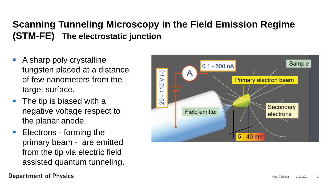
A sharp poly crystalline
tungsten placed at a distance
of few nanometers from the
target surface.
The tip is biased with a
negative voltage respect to
the planar anode.
Electrons - forming the
primary beam - are emitted
from the tip via electric field
assisted quantum tunneling.
Hugo Cabrera 2
1.12.2014
Scanning Tunneling Microscopy in the Field Emission Regime
(STM-FE) The electrostatic junction
3
The tip is moved parallel to
the surface and the low
energy primary electron
beam is scattered by the
target surface generating
secondary electrons (SE).
The SE are sampled by a
suitable electron current
measuring instrument placed
in the vicinity of the tip-
surface junction.
Hugo Cabrera3
10.10.2016
Scanning Tunneling Microscopy in the Field Emission Regime
(STM-FE) First results
4Hugo Cabrera 4
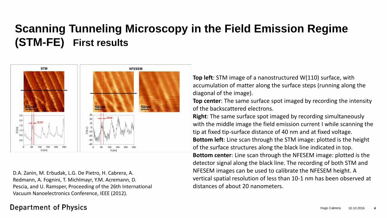
Top left: STM image of a nanostructured W(110) surface, with accumulation of matter along the surface steps (running along the diagonal of the image).Top center: The same surface spot imaged by recording the intensity of the backscattered electrons.Right: The same surface spot imaged by recording simultaneously with the middle image the field emission current I while scanning the tip at fixed tip-surface distance of 40 nm and at fixed voltage.Bottom left: Line scan through the STM image: plotted is the height of the surface structures along the black line indicated in top.Bottom center: Line scan through the NFESEM image: plotted is the detector signal along the black line. The recording of both STM and NFESEM images can be used to calibrate the NFESEM height. A vertical spatial resolution of less than 10-1 nm has been observed at distances of about 20 nanometers.
D.A. Zanin, M. Erbudak, L.G. De Pietro, H. Cabrera, A. Redmann, A. Fognini, T. Michlmayr, Y.M. Acremann, D. Pescia, and U. Ramsper, Proceeding of the 26th International Vacuum Nanoelectronics Conference, IEEE (2012).
1.12.2014
Scanning Tunneling Microscopy in the Field Emission Regime
(STM-FE) First results
5
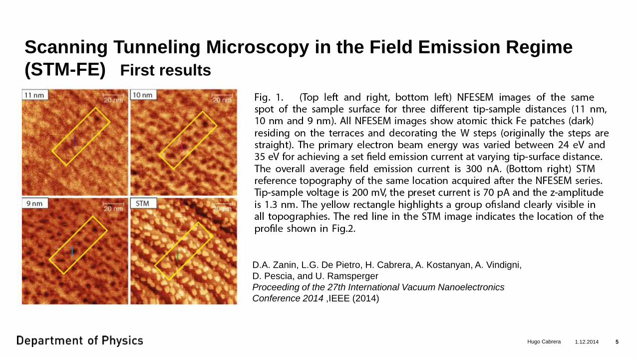
D.A. Zanin, L.G. De Pietro, H. Cabrera, A. Kostanyan, A. Vindigni,
D. Pescia, and U. Ramsperger
Proceeding of the 27th International Vacuum Nanoelectronics
Conference 2014 ,IEEE (2014)
Hugo Cabrera 5
1.12.2014
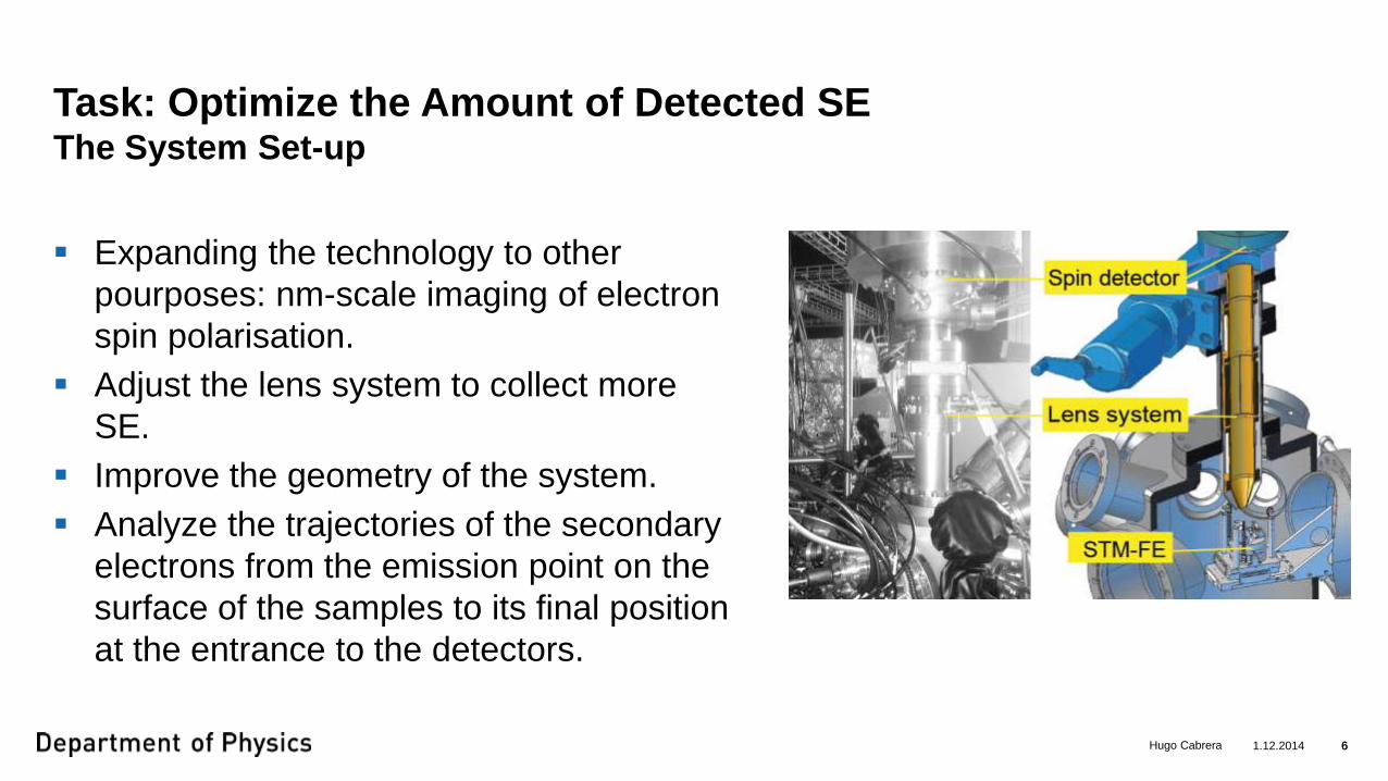
Expanding the technology to other
pourposes: nm-scale imaging of electron
spin polarisation.
Adjust the lens system to collect more
SE.
Improve the geometry of the system.
Analyze the trajectories of the secondary
electrons from the emission point on the
surface of the samples to its final position
at the entrance to the detectors.
Task: Optimize the Amount of Detected SEThe System Set-up
6Hugo Cabrera 6
10.10.2016Hugo Cabrera 7
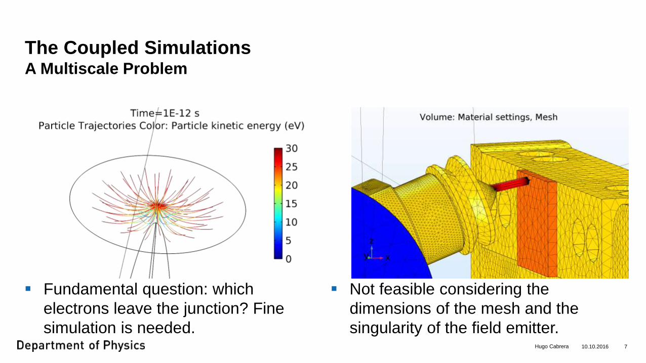
The Coupled SimulationsA Multiscale Problem
Fundamental question: which
electrons leave the junction? Fine
simulation is needed.
Not feasible considering the
dimensions of the mesh and the
singularity of the field emitter.
10.10.2016Hugo Cabrera 8
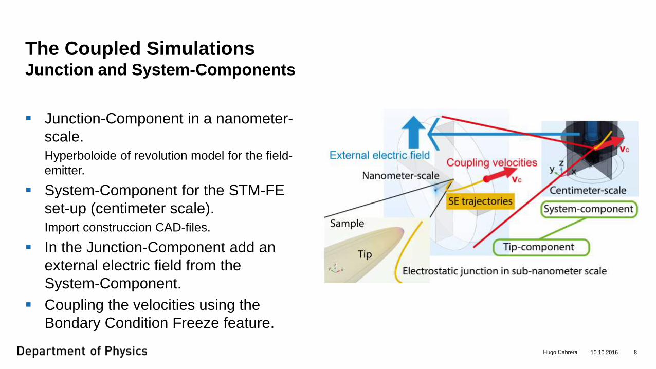
The Coupled SimulationsJunction and System-Components
Junction-Component in a nanometer-
scale.
Hyperboloide of revolution model for the field-
emitter.
System-Component for the STM-FE
set-up (centimeter scale).
Import construccion CAD-files.
In the Junction-Component add an
external electric field from the
System-Component.
Coupling the velocities using the
Bondary Condition Freeze feature.
10.10.2016Hugo Cabrera 9
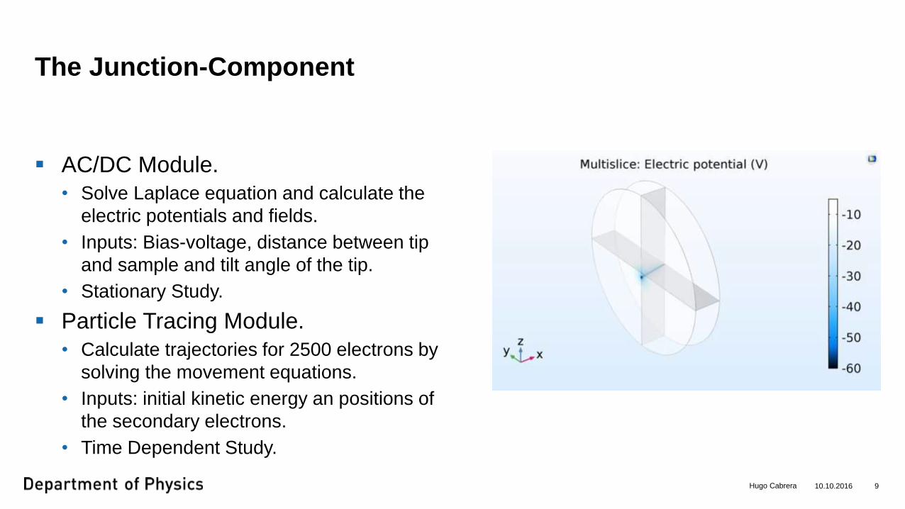
The Junction-Component
AC/DC Module.
• Solve Laplace equation and calculate the
electric potentials and fields.
• Inputs: Bias-voltage, distance between tip
and sample and tilt angle of the tip.
• Stationary Study.
Particle Tracing Module.
• Calculate trajectories for 2500 electrons by
solving the movement equations.
• Inputs: initial kinetic energy an positions of
the secondary electrons.
• Time Dependent Study.
10.10.2016Hugo Cabrera 10
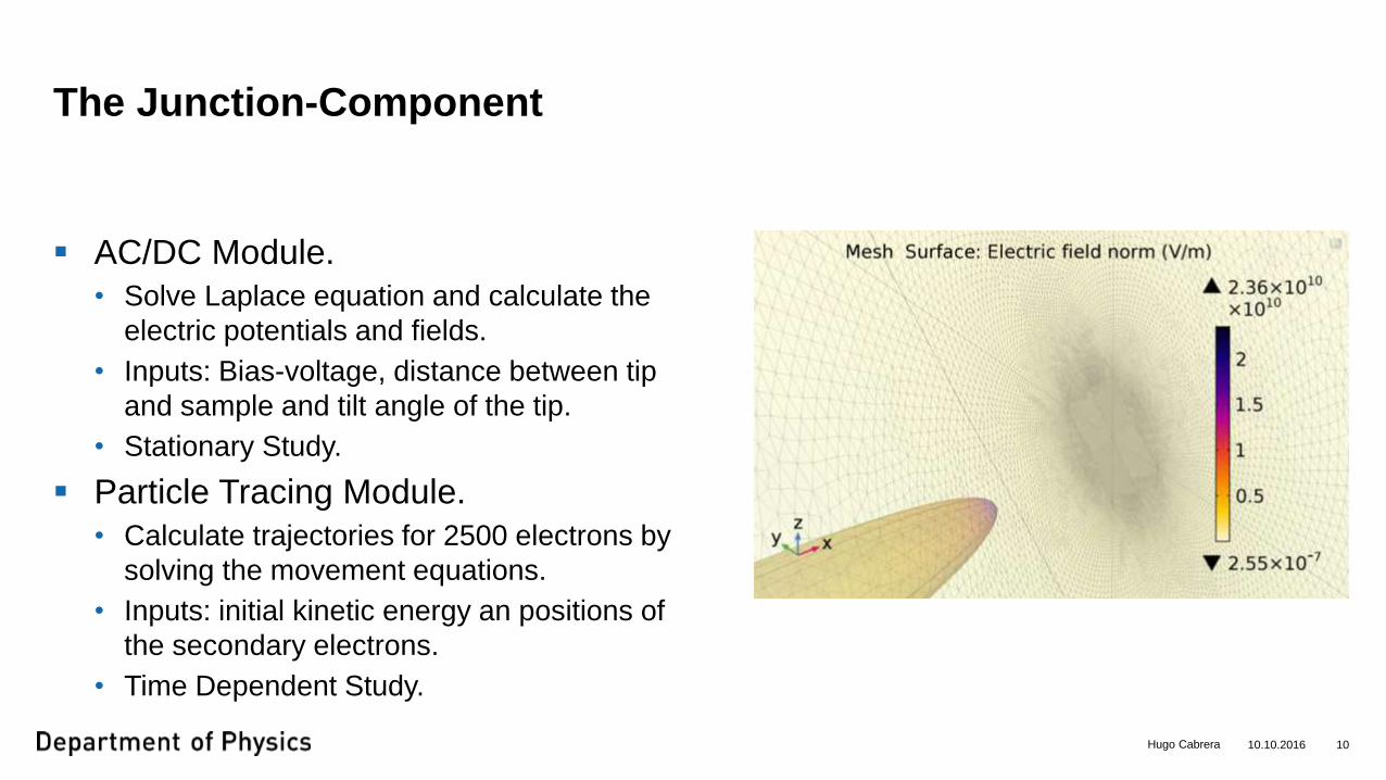
The Junction-Component
AC/DC Module.
• Solve Laplace equation and calculate the
electric potentials and fields.
• Inputs: Bias-voltage, distance between tip
and sample and tilt angle of the tip.
• Stationary Study.
Particle Tracing Module.
• Calculate trajectories for 2500 electrons by
solving the movement equations.
• Inputs: initial kinetic energy an positions of
the secondary electrons.
• Time Dependent Study.
10.10.2016Hugo Cabrera 11
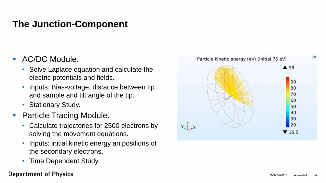
The Junction-Component
AC/DC Module.
• Solve Laplace equation and calculate the
electric potentials and fields.
• Inputs: Bias-voltage, distance between tip
and sample and tilt angle of the tip.
• Stationary Study.
Particle Tracing Module.
• Calculate trajectories for 2500 electrons by
solving the movement equations.
• Inputs: initial kinetic energy an positions of
the secondary electrons.
• Time Dependent Study.
12
The System-Component
10.10.2016Hugo Cabrera 12
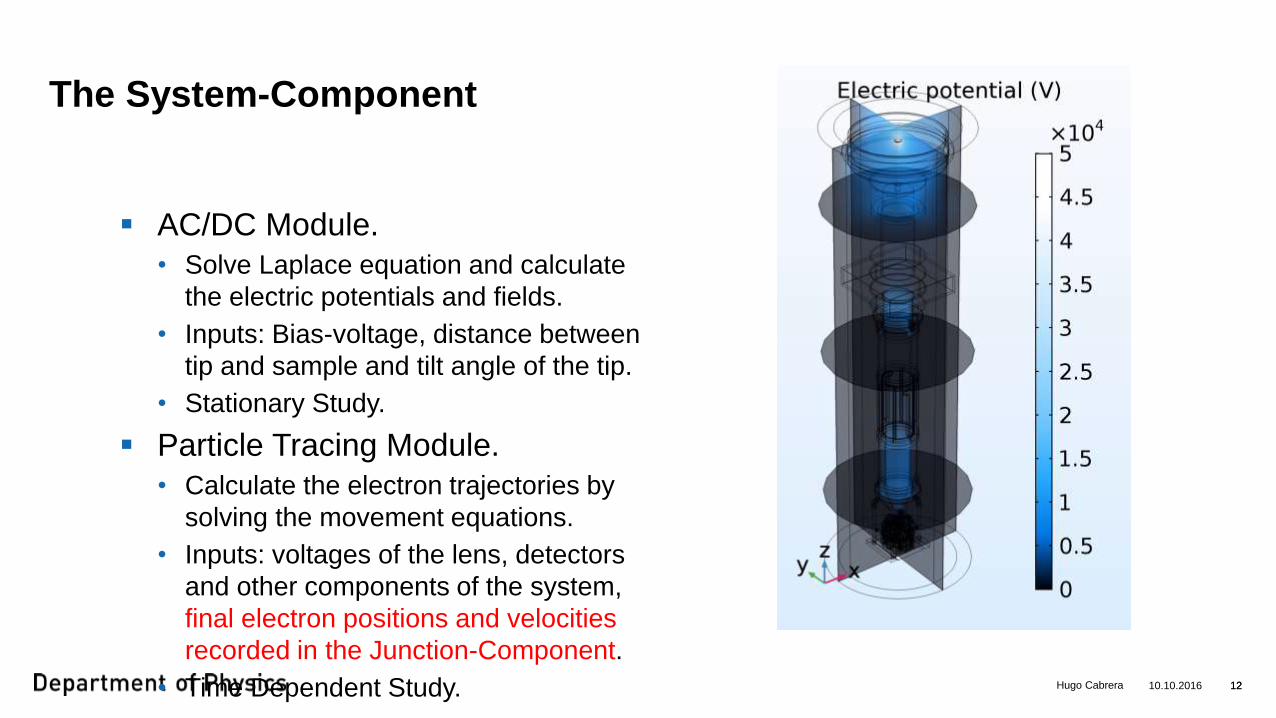
AC/DC Module.
• Solve Laplace equation and calculate
the electric potentials and fields.
• Inputs: Bias-voltage, distance between
tip and sample and tilt angle of the tip.
• Stationary Study.
Particle Tracing Module.
• Calculate the electron trajectories by
solving the movement equations.
• Inputs: voltages of the lens, detectors
and other components of the system,
final electron positions and velocities
recorded in the Junction-Component.
• Time Dependent Study.
13
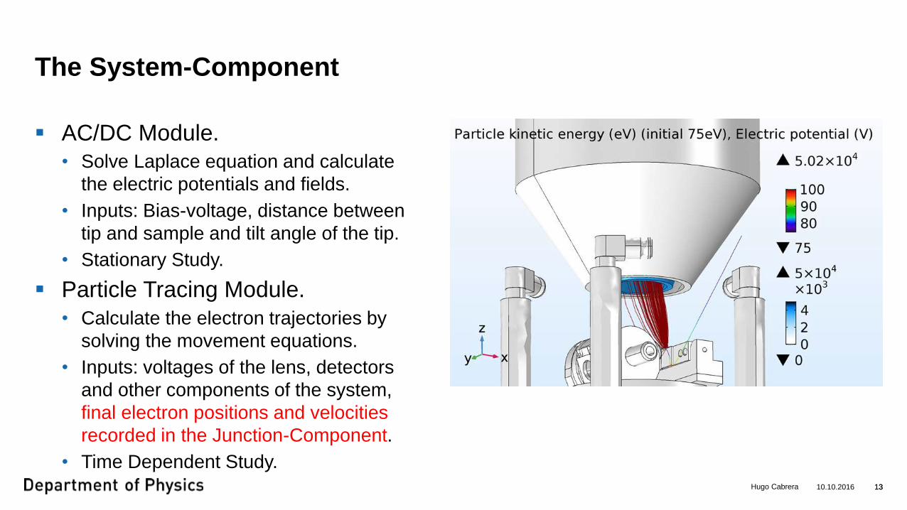
The System-Component
10.10.2016Hugo Cabrera 13
AC/DC Module.
• Solve Laplace equation and calculate
the electric potentials and fields.
• Inputs: Bias-voltage, distance between
tip and sample and tilt angle of the tip.
• Stationary Study.
Particle Tracing Module.
• Calculate the electron trajectories by
solving the movement equations.
• Inputs: voltages of the lens, detectors
and other components of the system,
final electron positions and velocities
recorded in the Junction-Component.
• Time Dependent Study.
14
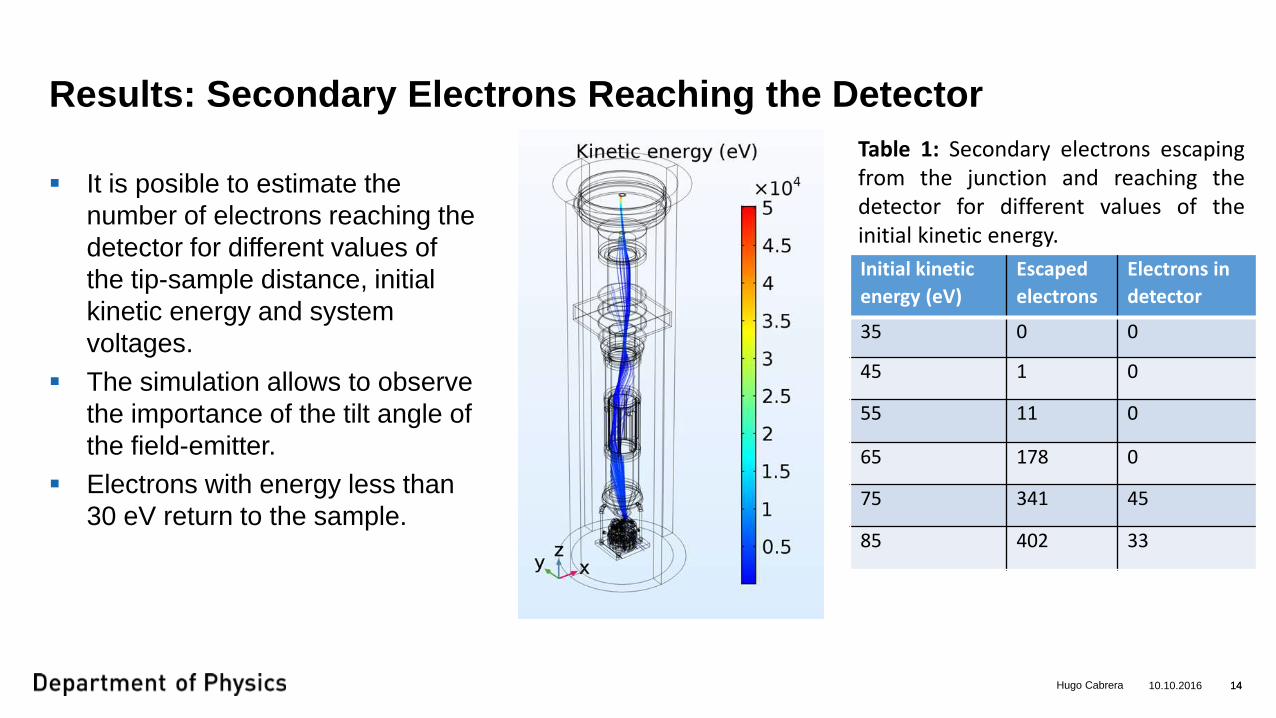
Results: Secondary Electrons Reaching the Detector
10.10.2016Hugo Cabrera 14
It is posible to estimate the
number of electrons reaching the
detector for different values of
the tip-sample distance, initial
kinetic energy and system
voltages.
The simulation allows to observe
the importance of the tilt angle of
the field-emitter.
Electrons with energy less than
30 eV return to the sample.
Table 1: Secondary electrons escapingfrom the junction and reaching thedetector for different values of theinitial kinetic energy.
Initial kinetic
energy (eV)
Escaped
electrons
Electrons in
detector
35 0 0
45 1 0
55 11 0
65 178 0
75 341 45
85 402 33
||Placeholder for organisational unit name / logo
(edit in slide master via “View” > “Slide Master”)