UNIVERSIT ` A DEGLI STUDI DI TRIESTE xxvii ciclo del dottorato di ricerca in nanotecnologie SELF-ASSEMBLY E CHIMICA DI SUPERFICIE DI SEMICONDUTTORI ORGANICI SU TiO 2 settore scientifico-disciplinare: fis/03 – Fisica della Materia studente Giacomo Lovat direttore della scuola Prof.ssa Lucia Pasquato supervisore Prof. Alberto Morgante tutore Dr. Luca Floreano ANNO ACCADEMICO 2013/2014
Transcript
UNIVERSITA DEGLI STUDI DI TRIESTE
xxvii ciclo del dottorato di ricerca in nanotecnologie
SELF-ASSEMBLY E CHIMICA DI
SUPERFICIE DI SEMICONDUTTORI
ORGANICI SU TiO2
settore scientifico-disciplinare: fis/03 – Fisica della Materia
studente
Giacomo Lovat
direttore della scuola
Prof.ssa Lucia Pasquato
supervisore
Prof. Alberto Morgante
tutore
Dr. Luca Floreano
ANNO ACCADEMICO 2013/2014
UNIVERSITA DEGLI STUDI DI TRIESTE
xxvii ciclo del dottorato di ricerca in nanotecnologie
SELF-ASSEMBLY AND ON-SURFACE
CHEMISTRY OF ORGANIC
SEMICONDUCTORS ON TiO2
settore scientifico-disciplinare: fis/03 – Fisica della Materia
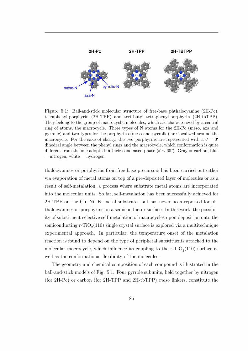
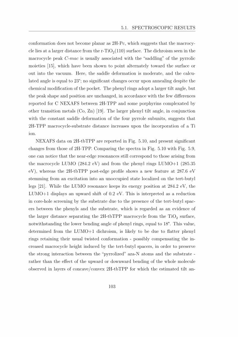
TPP) and tert-butyl tetraphenyl-porphyrin (2H-tbTPP), with special atten-
tion devoted to correlating the differences in the electronic structure and
chemical reactivity to the specific conformation of the heterocycles.
The power of scanning tunneling microscopy (STM), a technique capable of
imaging the local electronic structure and self-assembly patterns of adsorbates
3
in the real space, has been combined with the surface sensitivity and chemical
selectivity of X-ray photoelectron spectroscopy (XPS) and near-edge absorption
(NEXAFS) with synchrotron radiation, which reveal the chemical composition and
bonding of the thin film. In addition, density functional theory (DFT) calcula-
tions are presented for some interfaces as a result of the joint experimental and
theoretical approach adopted in collaboration with two research groups working
on condensed matter simulations. Numerical simulations are not only a valu-
able aid to the interpretation of the experimental measurements, they also test
the reliability and limits of the selected density functional in describing the or-
ganic/semiconductor interaction.
Chapter 2 provides a short introduction to the experimental techniques and
apparatus. Chapter 3 presents the geometry, electronic structure and STM ap-
pearance of the r-TiO2(110)-1×1 surface as well as the structure and appearance
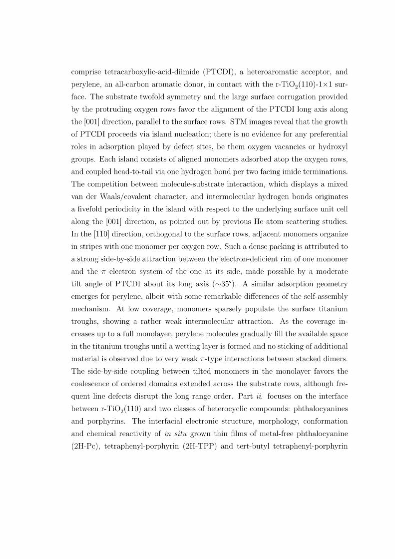
of its 1×2 cross-linked reconstruction. Chapter 4 is devoted to the study of PTCDI
and perylene. Chapter 5 expounds the measurements on the heterocyclic macrocy-
cles 2H-Pc, 2H-TPP and 2H-tbTPP and report a discussion of the results. Finally,
Chapter 6 summarizes the conclusions.
4
1.1. REFERENCES (INTRODUCTION)
1.1 References (Introduction)
[1] Howard E Katz and Jia Huang.
Thin-film organic electronic de-
vices. Annual Review of Materials
Research, 39:71–92, 2009.
[2] Antonio Facchetti. Semiconductors
for organic transistors. Materials
Today, 10(3):28–37, 2007.
[3] Colin Reese, Mark Roberts, Mang-
mang Ling, and Zhenan Bao. Or-
ganic thin film transistors. Materi-
als today, 7(9):20–27, 2004.
[4] Ali Safiei, Jorg Henzl, and Karina
Morgenstern. Isomerization of an
azobenzene derivative on a thin in-
sulating layer by inelastically tun-
neling electrons. Phys. Rev. Lett.,
104:216102, May 2010.
[5] Jascha Repp, Gerhard Meyer,
Fredrik E Olsson, and Mats Pers-
son. Controlling the charge state of
individual gold adatoms. Science,
305(5683):493–495, 2004.
[6] Fabian Mohn, Leo Gross, Nikolaj
Moll, and Gerhard Meyer. Imag-
ing the charge distribution within
a single molecule. Nature nanotech-
nology, 7(4):227–231, 2012.
[7] Jascha Repp, Gerhard Meyer, Sami
Paavilainen, Fredrik E Olsson, and
Mats Persson. Imaging bond for-
mation between a gold atom and
pentacene on an insulating sur-
face. Science, 312(5777):1196–
1199, 2006.
5
1.1. REFERENCES (INTRODUCTION)
6
2 Experimental techniques
and apparatus
2.1 Scanning tunneling microscopy
Scanning probe methods are based on the measurement of specific physical quanti-
ties performed by a sharp tip placed in the proximity of a sample surface. Scanning
tunneling microscopy, STM, was a major scientific breakthrough that allowed the
investigation of both the surface charge distribution of conducting materials at
the atomic scale. The technique measures the electron tunneling current which
flows between the tip and the sample surface once a bias voltage has been applied.
Nowadays it is a well-established technique, and commercially available micro-
scopes greatly improved their performances in terms of vibration isolation of the
probe and sample, which leads to a superior tip stability. Unlike diffraction, STM
provides a real space visualization of the atomic geometry, but it does not “see”
the atoms directly. Only electronic states are accessible with STM; since they
are correlated to the positions of atomic nuclei, the resulting electronic picture
of a surface, whenever atomic resolution is achieved, can reveal the geometrical
arrangement of the atoms in the outermost layer.
The real space, high-precision imaging realized with the STM offers attractive
advantages:
information on the shallow electronic structure of surfaces or adsorbates can
be gathered by recording and analyzing I -V curves or by switching the sign
of the bias voltage to enable the visualization of either filled or empty orbitals
7
2.1. SCANNING TUNNELING MICROSCOPY
the possibility of studying the dynamics of slow chemical reactions at sur-
faces with a direct access to the visualization of orbitals involved in chemical
bonding
the use of nanomanipulation for moving atoms or molecules, and building
functional nano-assemblies through tip-induced bond formation or cleavage
the study of complex self-assembled patterns produced by molecules with
chemically heterogeneous functional moieties
Finally, one must emphasize the versatility of the technique. In addition to the
ultra-high vacuum environment required for surface science, STM can operate in
ambient conditions and in liquid, opening the door for the nano-characterization
of biological matter.
2.1.1 Vacuum tunneling
To illustrate the concept underlying the STM operation and its high vertical res-
olution, a simple model of quantum tunneling between the tip and the sample is
introduced [1] by treating the interposed vacuum layer as a square potential bar-
rier. We assume that both tip and sample are metals. In classical physics, the
spatial region covered by a potential barrier is forbidden for particles whose kinetic
energy is less than the energy of the barrier. In quantum mechanics, an electron
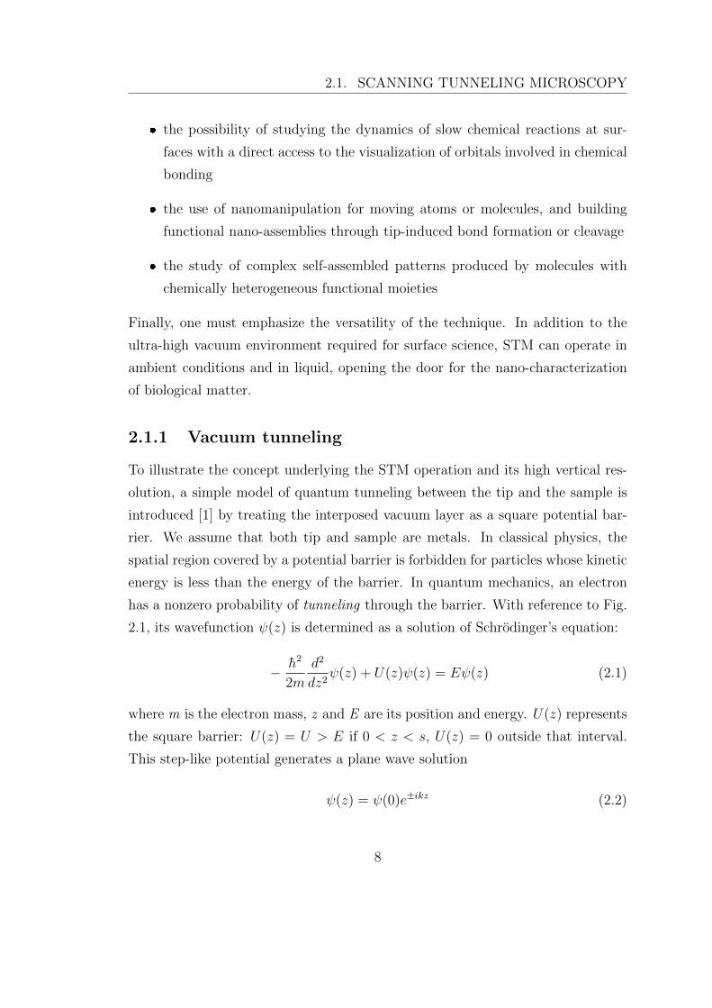
has a nonzero probability of tunneling through the barrier. With reference to Fig.
2.1, its wavefunction ψ(z) is determined as a solution of Schrodinger’s equation:
− h2
2m
d2
dz2ψ(z) + U(z)ψ(z) = Eψ(z) (2.1)
where m is the electron mass, z and E are its position and energy. U(z) represents
the square barrier: U(z) = U > E if 0 < z < s, U(z) = 0 outside that interval.
This step-like potential generates a plane wave solution
ψ(z) = ψ(0)e±ikz (2.2)
8
2.1. SCANNING TUNNELING MICROSCOPY
Figure 2.1: One-dimensional sample-vacuum-tip square barrier and eigenfunction of thetunneling problem (after [1]).
in the classically allowed region E > U(z), where
k =
√2m(E − U)
h(2.3)
is the wave vector. The electron moves with a constant momentum pz = hk =√2m(E − U). In the region where E < U(z), the solution is an exponentially
damped probability density:
ψ(z) = ψ(0)e−κz, (2.4)
where the decay constant is
κ =
√2m(U − E)
h(2.5)
hence, the electron has a finite probability |ψ(s)|2 = |ψ(0)|2e−2κs of crossing the
barrier and being detected at z = s. Let us reference the energies to the vacuum
energy of an electron far from the sample surface by setting it to zero. The electrons
at the sample Fermi level have energy EF , while the energy required to extract
one electron from the surface, so that it escapes with zero kinetic energy, is the
work function φ. We assume that the tip and the sample have the same work
function; typical values for noble metals are 4-5 eV, while alkali metals have φ ∼
9
2.1. SCANNING TUNNELING MICROSCOPY
2-3 eV. When the tip is placed near the sample surface, in absence of any applied
voltages, no current flows through the junction. When a voltage V is applied, e.g.
a positive voltage to the tip, the electrons in the sample with energy between EF
and EF−eV may penetrate the vacuum barrier and occupy the empty levels of the
tip. If the voltage is much smaller than the sample work function eV << φ, the
energy of the tunneling electrons is approximately equal to −φ. The probability
of an electron occupying the n-th state in this energy region to cross the barrier
and present at the tip surface is w ∝ |ψ(0)|2e−2κs, and
κ =
√2mφ
h(2.6)
is the decay constant of a sample state near the Fermi level in the barrier region.
The decay constant may be written in units of A−1 as
κ = 0.51√φ(eV) A
−1(2.7)
In stable tunneling conditions, the tip does not change with time and the electron
flow is stationary. The tunneling current is thus proportional to the sample density
of electronic states near the Fermi level. An expression for the total current must
include the contributions of all the electronic states in the energy window [EF −eV,EF ]:
I ∝ V
∫ EF
EF−eVdEρ(E, 0)|ψ(z = 0)|2 (2.8)
where ρ(E, z = 0) represents the density of electronic states as a function of their
energy at the sample surface. Provided that the voltage is sufficiently small, we
obtain the tunneling current dependence on the density of states at the Fermi level
of the sample surface:
I ∝ V ρ(EF , 0)e−2κs. (2.9)
Using the typical value of 4 eV for the work function, the decay constant 2.6
becomes κ ∼ 1 A−1
. Therefore, according to the above formula, the current
decays about e2 = 7.4 times when the tip is moved away from the surface by just
10
2.1. SCANNING TUNNELING MICROSCOPY
1 A.
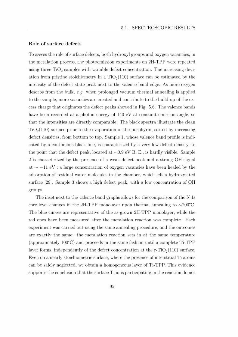
The one-dimensional constant-height potential is a rough approximation to the
vacuum barrier. Several effects contribute to the complexity of the tip-sample
system, e.g. the charge image potential due to the interaction between tunneling
electrons and the opposing electrode at which surface charge builds up, or the in-
herent many-body nature of the system, as electrons populating the valence states
of a crystal are mutually interacting charges. However, a general, more accurate
description of tunneling can be set forth using Bardeen’s formalism [2], provided
that certain conditions be satisfied: negligible interaction occurs between the two
electrodes, which can be assumed as independent, and tunneling is described by
a small coupling not perturbing the electron wavefunctions significantly. Under
these assumptions, the tunneling current can be written as:
I =4πe
h
∫dε [f(EF − eV + ε)− f(EF + ε)]×
ρS(EF − eV + ε)ρT (ET + ε)× |M |2 (2.10)
where the integral is calculated over the whole range of relevant energies. The
formula couples the probability distribution of electrons of energy E, f(E) =
1/ 1 + exp[(E − EF )/kBT ], to the electron density of the tip and the sample, ρT
and ρS; the transfer of electrons from filled to empty states is mediated by a matrix
element M . In the low-temperature limit kBT << eV , and if the matrix element
does not vary appreciably over the energy interval, the above formula becomes a
simple convolution of the density of states of the two electrodes:
I =4πe
h
∫ eV
0
dερS(EF − eV + ε)ρT (EF + ε) (2.11)
This is a basic approximation for modeling the STM contrast where tip states
are explicitly accounted for, although the tip geometry is highly simplified: it
is a homogeneous crystal, with no spatial boundaries. Note that the tip and
sample densities of states are equally represented in Eq. 2.11, which makes them
interchangeable without modifying the resulting value of the current.
11
2.1. SCANNING TUNNELING MICROSCOPY
Figure 2.2: Schematic diagram of a scanning tunneling microscope (after [1]).
2.1.2 The S-symmetry wave tip model
The formula for the tunneling current when the tip geometry is modeled as a sphere
was worked out by Tersoff and Haman [3], starting from Eq. 2.10. They considered
a spherical potential well and an S -symmetry wave approximation of the wavefunc-
tion (ψ(r) ∼ e−r/r) to calculate the matrix element M. These assumptions lead to
the simple result:
I ∝ eV · ρS(r0, EF ) (2.12)
the tunneling current, at low bias, is proportional to the Fermi level density of
states at the center of curvature of the tip r0. Therefore, in the S -symmetry wave
model, the contour map of the local density of states at the Fermi level (LDOS)
on the sample surface represents the STM current taken at the center of curvature
of the tip r0. Eq. 2.12 provides a valuable, albeit basic, approximation, which can
be applied to interpret the STM contrast.
2.1.3 The experimental setup
Fig. 2.2 illustrates the components of an STM apparatus. High-precision move-
ments along the three spatial directions are enabled by three piezoelectric motors,
which constitute the piezodrive and expand or contract upon applying a voltage.
12
2.1. SCANNING TUNNELING MICROSCOPY
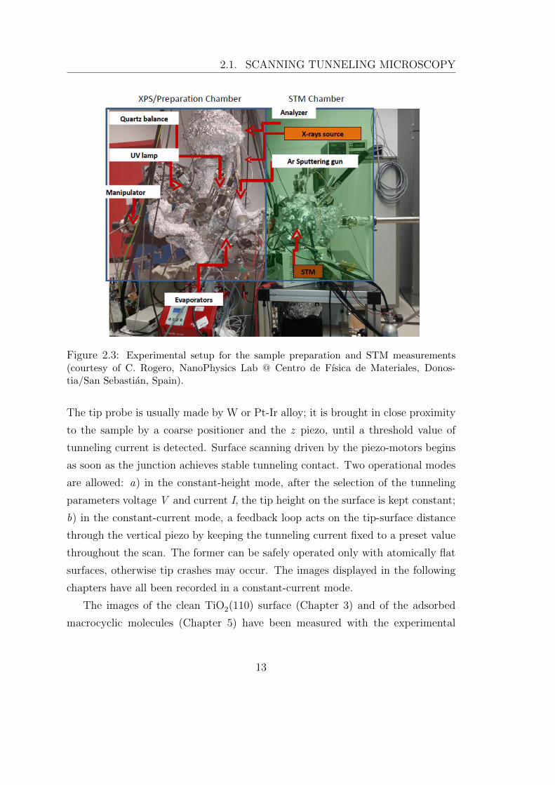
Figure 2.3: Experimental setup for the sample preparation and STM measurements(courtesy of C. Rogero, NanoPhysics Lab @ Centro de Fısica de Materiales, Donos-tia/San Sebastian, Spain).
The tip probe is usually made by W or Pt-Ir alloy; it is brought in close proximity
to the sample by a coarse positioner and the z piezo, until a threshold value of
tunneling current is detected. Surface scanning driven by the piezo-motors begins
as soon as the junction achieves stable tunneling contact. Two operational modes
are allowed: a) in the constant-height mode, after the selection of the tunneling
parameters voltage V and current I, the tip height on the surface is kept constant;
b) in the constant-current mode, a feedback loop acts on the tip-surface distance
through the vertical piezo by keeping the tunneling current fixed to a preset value
throughout the scan. The former can be safely operated only with atomically flat
surfaces, otherwise tip crashes may occur. The images displayed in the following
chapters have all been recorded in a constant-current mode.
The images of the clean TiO2(110) surface (Chapter 3) and of the adsorbed
macrocyclic molecules (Chapter 5) have been measured with the experimental
13
2.1. SCANNING TUNNELING MICROSCOPY
setup photographed in Fig. 2.3; the images of PTCDI/perylene have instead been
recorded at Prof. Martın-Gago’s STM facility (ESISNA group, CSIC @ Madrid),
where a LEED (low-energy electron diffraction) apparatus was part of the exper-
imental setup, allowing a quick assessment of the substrate cleanliness and of the
growth of the desired phase in self-assembled molecular films. Two experimen-
tal stages, the chamber hosting the microscope and the preparation chamber, are
separated by a vacuum valve to prevent the contamination of the high vacuum in
the STM chamber, where a base pressure of 1× 10⁻¹⁰ mbar is needed in order to
keep the surface free of impurities for a long time. The preparation chamber is
equipped with:
(1) one ion gun for cleaning the sample with Ar ion sputtering
(2) a set of filament-heated crucibles (evaporators) filled with high-purity organic
compounds in powder form, to be degassed and subsequently sublimed on
the sample
(3) a quartz microbalance to monitor the flux of molecules from the crucibles
(4) one He I ultraviolet lamp (21.2 eV) and one X-ray source (Al K-α radiation,
1486.6 eV) to characterize the sample with photoemission spectroscopy
(5) one spherical electron energy analyzer
(6) a sample transfer arm, protruding from the left side of the chamber, and a
manipulator. Both are mechanical arms manually operated; the manipula-
tor hosts the sample for molecular-beam epitaxy and provides a grounded
support for photoemission measurements. Its back accommodates a filament
for sample heating.
The STM chamber hosts the probe, a second transfer arm and a sample holder
where the bias voltage is applied once the sample has been deposited from the
transfer arm. Aside from the screening of electrical noise, one very important
factor for the achievement of atomic resolution and tunneling stability is a care-
ful isolation from mechanical vibrations, which are effectively damped by spring
suspensions attached to the tip-sample system.
14
2.2. ELECTRON SPECTROSCOPIES
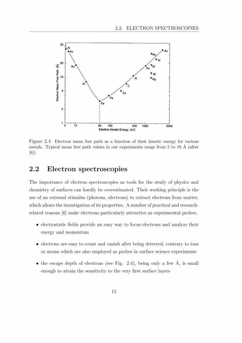
Figure 2.4: Electron mean free path as a function of their kinetic energy for variousmetals. Typical mean free path values in our experiments range from 5 to 10 A (after[6]).
2.2 Electron spectroscopies
The importance of electron spectroscopies as tools for the study of physics and
chemistry of surfaces can hardly be overestimated. Their working principle is the
use of an external stimulus (photons, electrons) to extract electrons from matter,
which allows the investigation of its properties. A number of practical and research-
related reasons [6] make electrons particularly attractive as experimental probes:
electrostatic fields provide an easy way to focus electrons and analyze their
energy and momentum
electrons are easy to count and vanish after being detected, contrary to ions
or atoms which are also employed as probes in surface science experiments
the escape depth of electrons (see Fig. 2.4), being only a few A, is small
enough to attain the sensitivity to the very first surface layers
15
2.2. ELECTRON SPECTROSCOPIES
electrons provide direct information on the electronic structure of matter,
and the amazing properties which derive from it (e.g. superconductivity).
Apart from resolving the band structure of a crystal and enabling the study of
chemical reactions on a surface, electron spectroscopies also give insight into ge-
ometric features like the orientation and adsorption sites of adsorbates, or the
environment around one specific atomic species in a crystal. In that respect, they
play a valuable complementary role when coupled to scanning probe microscopies.
They unravel the chemical composition of adlayers and are sensitive to the pres-
ence of small amounts of chemical species which can hardly be identified through
the analysis of STM topography. An exhaustive introduction to the variety of
available techniques is beyond the scope of this section, therefore only the ones
which have been extensively used throughout the research work will be discussed.
A distinction into two classes is made according to the type of information on
the electronic structure of matter which is accessed: a) X-ray photoemission spec-
troscopy probes the filled electronic states; b) near-edge X-ray absorption probes
the empty states.
2.2.1 Soft X-ray photoemission
Electrons in a crystal may display core- or valence-like character depending
on whether they are best approximated by orbitals confined in the vicinity of
atom cores or delocalized over the crystal to participate to interatomic bonds.
Figure 2.5: Schematic diagram of a photoemission measurement (after [5]).
16
2.2. ELECTRON SPECTROSCOPIES
Photoemission spectroscopy provides access to both core and valence electrons by
means of light-stimulated electron ejection from bound states into the vacuum.
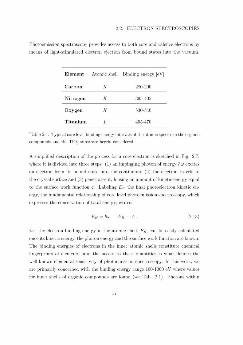
Element Atomic shell Binding energy [eV]
Carbon K 280-290
Nitrogen K 395-405
Oxygen K 530-540
Titanium L 455-470
Table 2.1: Typical core level binding energy intervals of the atomic species in the organic
compounds and the TiO2 substrate herein considered.
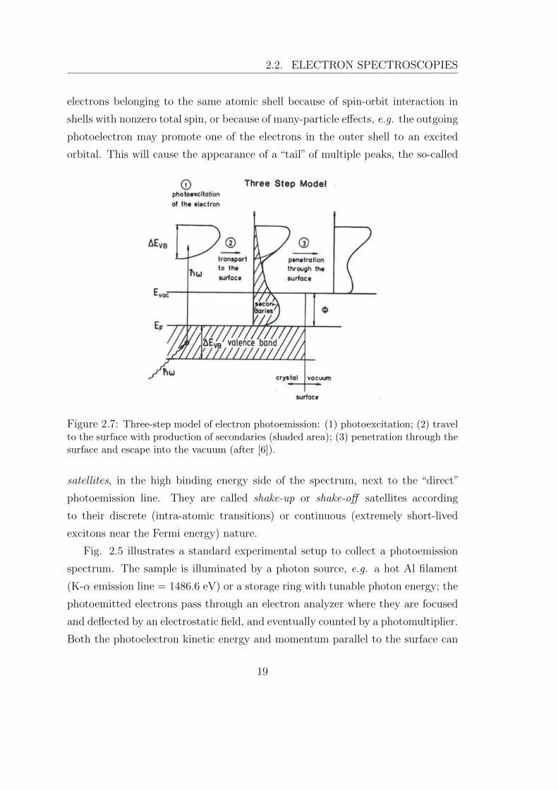
A simplified description of the process for a core electron is sketched in Fig. 2.7,
where it is divided into three steps: (1) an impinging photon of energy hω excites
an electron from its bound state into the continuum; (2) the electron travels to
the crystal surface and (3) penetrates it, loosing an amount of kinetic energy equal
to the surface work function φ. Labeling EK the final photoelectron kinetic en-
ergy, the fundamental relationship of core level photoemission spectroscopy, which
expresses the conservation of total energy, writes:
EK = hω − |EB| − φ , (2.13)
i.e. the electron binding energy in the atomic shell, EB, can be easily calculated
once its kinetic energy, the photon energy and the surface work function are known.
The binding energies of electrons in the inner atomic shells constitute chemical
fingerprints of elements, and the access to these quantities is what defines the
well-known elemental sensitivity of photoemission spectroscopy. In this work, we
are primarily concerned with the binding energy range 100-1000 eV where values
for inner shells of organic compounds are found (see Tab. 2.1). Photons within
17
2.2. ELECTRON SPECTROSCOPIES
this energy range, the so-called soft regime, have a probe depth on the order of 1
µm, well beyond the surface layer. However, the kinetic energies of photoemitted
electrons from core levels have typical values between 100 and 500 eV, which
translates into mean free paths between 5 and 10 A, as reported in the graph of
Fig. 2.4. As a result, the sensitivity of photoelectrons is limited to the outermost
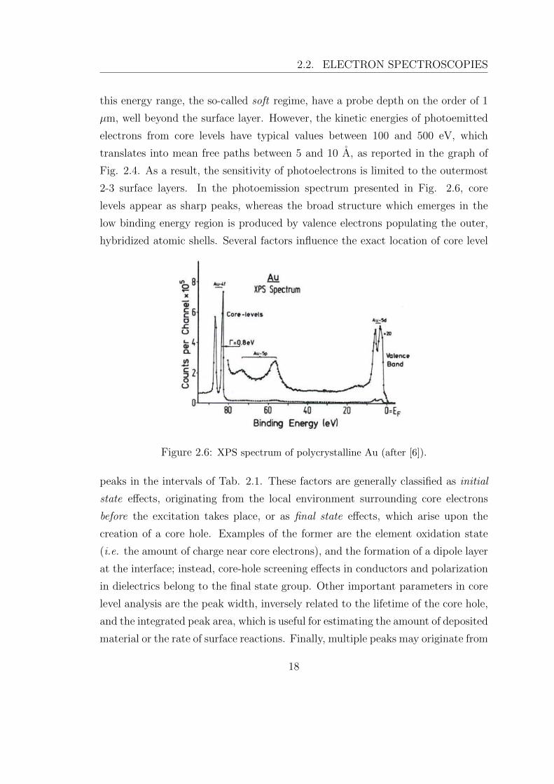
2-3 surface layers. In the photoemission spectrum presented in Fig. 2.6, core
levels appear as sharp peaks, whereas the broad structure which emerges in the
low binding energy region is produced by valence electrons populating the outer,
hybridized atomic shells. Several factors influence the exact location of core level
Figure 2.6: XPS spectrum of polycrystalline Au (after [6]).
peaks in the intervals of Tab. 2.1. These factors are generally classified as initial
state effects, originating from the local environment surrounding core electrons
before the excitation takes place, or as final state effects, which arise upon the
creation of a core hole. Examples of the former are the element oxidation state
(i.e. the amount of charge near core electrons), and the formation of a dipole layer
at the interface; instead, core-hole screening effects in conductors and polarization
in dielectrics belong to the final state group. Other important parameters in core
level analysis are the peak width, inversely related to the lifetime of the core hole,
and the integrated peak area, which is useful for estimating the amount of deposited
material or the rate of surface reactions. Finally, multiple peaks may originate from
18
2.2. ELECTRON SPECTROSCOPIES
electrons belonging to the same atomic shell because of spin-orbit interaction in
shells with nonzero total spin, or because of many-particle effects, e.g. the outgoing
photoelectron may promote one of the electrons in the outer shell to an excited
orbital. This will cause the appearance of a “tail” of multiple peaks, the so-called
Figure 2.7: Three-step model of electron photoemission: (1) photoexcitation; (2) travelto the surface with production of secondaries (shaded area); (3) penetration through thesurface and escape into the vacuum (after [6]).
satellites, in the high binding energy side of the spectrum, next to the “direct”
photoemission line. They are called shake-up or shake-off satellites according
to their discrete (intra-atomic transitions) or continuous (extremely short-lived
excitons near the Fermi energy) nature.
Fig. 2.5 illustrates a standard experimental setup to collect a photoemission
spectrum. The sample is illuminated by a photon source, e.g. a hot Al filament
(K-α emission line = 1486.6 eV) or a storage ring with tunable photon energy; the
photoemitted electrons pass through an electron analyzer where they are focused
and deflected by an electrostatic field, and eventually counted by a photomultiplier.
Both the photoelectron kinetic energy and momentum parallel to the surface can
19
2.2. ELECTRON SPECTROSCOPIES
be determined. Usual requirements needed to perform high-resolution soft X-ray
photoemission on thin films of thickness between 1 and 10 molecular layers are
an ultra-high vacuum environment (∼ 10−10 mbar), since air molecules rapidly
stick onto a clean sample surface, a geometry enhancing the surface sensitivity,
e.g. by collecting photoelectrons at a grazing emission angle, and the availability
of brilliant and tunable photon sources which make several core lines accessible
with a high cross section for photoabsorption.
2.2.2 Near-edge X-ray absorption
If the energy of the incoming photon matches the energy difference between a core
state and an empty state, a resonant excitation of the core electron into the empty
orbital can occur. The excited system decays via either the emission of a photon
of lower energy, a process called fluorescence, or the emission of an Auger electron
(see Fig. 2.8). Both decays can be exploited for recording the near-edge X-ray ab-
sorption fine structure (NEXAFS): the electrons emitted upon each core-to-valence
transition and subsequent de-excitation are collected by sweeping the photon en-
ergy across a short interval where the empty state energies, in the presence of
a core hole, are located. However, the strong predominance of Auger emission
over fluorescence for the lighter elements (Z < 35) [9] makes Auger electrons a
convenient tool to explore the electronic and structural properties of organic thin
films.
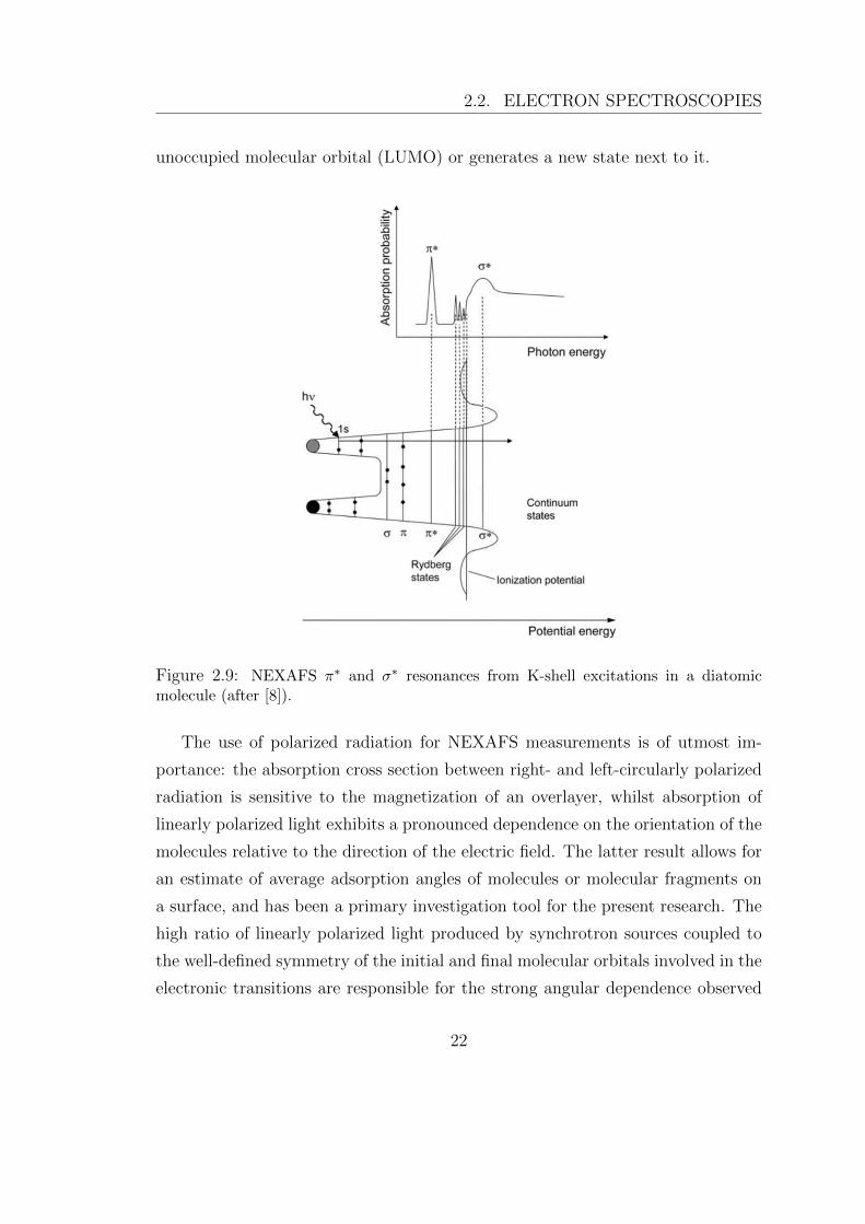
A schematic NEXAFS peak profile for a diatomic molecule is drawn in Fig. 2.9.
It shows three types of resonances, grouped on the basis of their shape and position
with reference to the ionization energy of the molecule. The first intense and nar-
row feature located close to the absorption threshold corresponds to the excitation
of a core electron into a π∗ orbital, i.e. an orbital symmetric by reflection upon a
nodal plane, which is often the lowest unoccupied orbital in an organic molecule.
Several sharp but less intense peaks accompany the 1s → π∗ transition, which
are associated with Rydberg orbitals; these resonances are generally quenched in
adsorbed molecules due to their large spatial extent which favors a fast delocaliza-
tion (hence energy broadening) of the excited electron into the empty states of the
20
2.2. ELECTRON SPECTROSCOPIES
Figure 2.8: Sketch of photoexcitation from an atom K-shell and subsequent de-excitation paths: (A) One core electron is excited into an unoccupied state, leavingbehind a core hole. The excited atom decays to its ground state either by (B) emissionof a photon (fluorescence) or (C, D) emission of an Auger electron in the participator orspectator modes.
substrate. Excitations into σ∗ empty orbitals, characterized by a mirror symmetry
axis, occur at higher photon energies, since σ∗ orbitals are usually found above the
vacuum level for neutral molecules. As a consequence, the lifetime of the excited
state is reduced, and σ∗ resonances appear significantly broader.
NEXAFS spectra can give a view of the structural organization of an overlayer,
its magnetic properties and bonding. For instance, bond lengths in a molecule
can be estimated through the analysis of the energy position of σ∗ resonances.
Since this quantity is also sensitive to the oxidation state of an atom, chemical
reactions on surfaces may easily be monitored. Furthermore, the chemisorption
state of a molecule is often recognized by the occurrence of a molecule-substrate
charge transfer which either quenches the NEXAFS peak associated with the lowest
21
2.2. ELECTRON SPECTROSCOPIES
unoccupied molecular orbital (LUMO) or generates a new state next to it.
Figure 2.9: NEXAFS π∗ and σ∗ resonances from K-shell excitations in a diatomicmolecule (after [8]).
The use of polarized radiation for NEXAFS measurements is of utmost im-
portance: the absorption cross section between right- and left-circularly polarized
radiation is sensitive to the magnetization of an overlayer, whilst absorption of
linearly polarized light exhibits a pronounced dependence on the orientation of the
molecules relative to the direction of the electric field. The latter result allows for
an estimate of average adsorption angles of molecules or molecular fragments on
a surface, and has been a primary investigation tool for the present research. The
high ratio of linearly polarized light produced by synchrotron sources coupled to
the well-defined symmetry of the initial and final molecular orbitals involved in the
electronic transitions are responsible for the strong angular dependence observed
22
2.2. ELECTRON SPECTROSCOPIES
in the resonance intensities. The intensity of a transition can be calculated with
the dipole matrix element derived from Fermi’s golden rule [9]
I ∝ | 〈f |E · er|i〉 |2 (2.14)
where E is the electric field of the incident photon, er represents the dipole opera-
tor, |i〉 is the electron initial state and |f〉 is its final state upon photoabsorption.
In the simplest case of photoabsorption by K-shell electrons, a 1s wavefunction is
taken as the initial state. For a final state orbital with p component pointing in
the direction represented by the vector O, one can write:
I ∝ |E · 〈f |r|ψ1s〉 |2 ∝ |ε ·O|2 ∝ cos2 δ (2.15)
with δ being the angle between the electric field vector E and the direction of the
final state orbital O. Because of the spatial localization of the 1s electrons, only
final states with significant p component on the specific atoms whose absorption
threshold is probed by the selected photon energy will appear in the spectrum.
This is the so-called dipole selection rule.
Figure 2.10: The electric field oscillates perpendicularly to the surface plane in P-polarized radiation, while it oscillates parallel to the plane in S-polarized radiation.Transitions to p-like empty orbitals, such as the delocalized π∗ antibonding orbitals inorganics, are dipole-allowed if the electric field vector of the impinging photon is collinearwith the orbital dipole.
Explicit formulas can be derived from Eq. 2.15 which allow the calculation
of the adsorption angle of a molecule on a surface of given symmetry. If one
considers a final π∗-plane molecular orbital, a fully linearly polarized photon beam
23
2.2. ELECTRON SPECTROSCOPIES
and a twofold-symmetric substrate, such as the (110) surfaces of FCC metals and
rutile-TiO2, the ratio between the intensities of a 1s → π∗ transition in S- and
P-polarized light becomes:
IS/IP = 1− cos2 θ cos2 γ − sin2 θ sin2 γ (2.16)
so that, assuming a small incidence angle θ, the equation yields:
IS/IP = tan2 γ (2.17)
For large molecules, one can view the separate molecular moieties as small
molecules joined by extra-molecular bonds similar to the intramolecular ones. One
may therefore envision the NEXAFS spectra of large molecules as the superposition
of resonances belonging to specific submolecular units where the core excitation
occurs; this approach is known as the building block principle. When the submolec-
ular units are allowed to take on multiple azimuthal orientations relative to the
molecular plane, e.g. aryl groups in meso-substituted porphyrins, the tilt angle
must be calculated with a formula for threefold or higher substrate symmetry:
IS/IP =3
2tan2 γ . (2.18)
Eq. 2.17 and 2.18 are valuable results to get insight into the average orientation
of molecules in self-assembled monolayers.
The experimental setup for a NEXAFS measurement resembles the one for
photoemission reported in Fig. 2.5. The sample surface is placed at grazing
incidence relative to the photon beam; the light polarization is switched by rotating
the sample about an axis parallel to the surface plane. The detection part can
differ from Fig. 2.5, as the NEXAFS signal can be collected in three modes:
a) total electron yield (TEY), by measuring the drain current generated in the
sample; b) Auger electron yield (AEY), by recording the elastically scattered Auger
electrons with an electron analyzer; and c) partial electron yield (PEY), where all
the outgoing Auger electrons with energy larger than a specified threshold are
24
2.3. THE ALOISA/HASPES BEAMLINE AT ELETTRA
Figure 2.11: Geometrical configuration showing the angles in Eq. 2.17 for a plane-type orbital. The cartesian axis z is taken orthogonal to the surface. O represents thedirection of the orbital plane.
counted by a channeltron, the less energetic ones being filtered out by a retarding
voltage. All the reported NEXAFS profiles have been measured in PEY mode.
2.3 The ALOISA/HASPES beamline at Elettra
ALOISA (Advanced Line for Over-layer, Interface and Surface Analysis) is a mul-
tipurpose beamline for surface science experiments. It was designed to work in
a wide spectral range from medium to hard X-rays and hosts two experimental
chambers: the first one, (original) ALOISA, is dedicated to X-ray diffraction and
X-ray spectroscopy experiments, while the second one, HASPES, additionally of-
fers ultraviolet spectroscopy and scattering of thermal He atoms. Fig. 2.12 shows
an outline of the whole experimental apparatus. A switching mirror is placed close
to the exit of the photon beam from the storage ring, to let the beam pass through
and enter the main ALOISA chamber or to deflect it, upon mirror insertion, to
the HASPES chamber.
The ALOISA photon beam is produced by the U7.2 wiggler/undulator insertion
device (ID) of the Elettra synchrotron. Two lines of magnets are superimposed
in a face-to-face configuration so as to form a series of collinear, adjacent dipoles
displaying opposite magnetization. The gap between the poles is user-tuned. As
the electrons travel through the oppositely-magnetized dipole lines, their path is
shaped into a wiggling curve by the magnetic dipolar fields. The light produced
25
2.3. THE ALOISA/HASPES BEAMLINE AT ELETTRA
Figure 2.12: Outline of the ALOISA/HASPES beamline at the Elettra synchrotronlight source (Trieste, Italy).
over the wiggling trajectory comes out of the pinhole separating the beamline
optics from the storage ring and consitutes the X-ray source of the beamline. Two
operational modes of the ID are allowed by the variation of the gap size between
the rows of facing magnets: the undulator mode in the region of high gap values
(∼ 40-80 mm) with low critical beam energy (100-2000 eV), and the wiggler mode
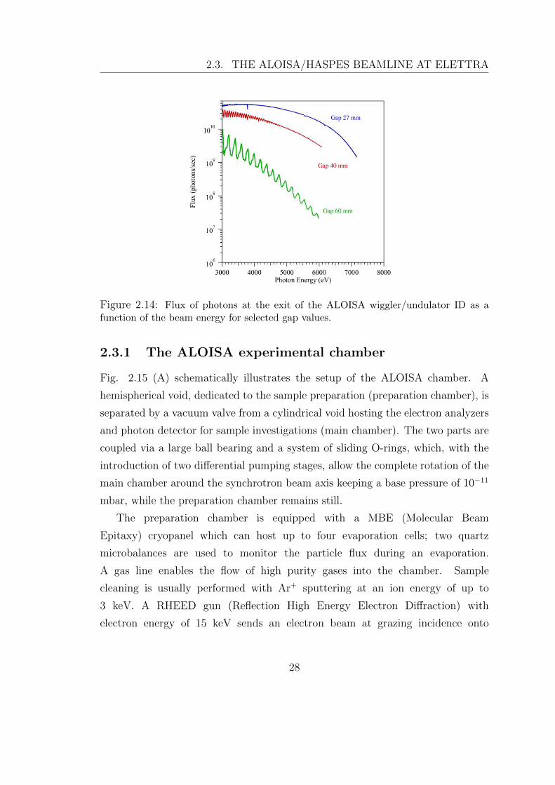
in the region of low gap values (∼ 20 mm) with high critical beam energy. Fig.
2.14 shows the intensity of the photon beam as a function of its energy, obtained
for different values of the ID gap. Small gap values lead to very dense oscillations
which make the intensity spectrum look like a bending magnet’s one. Synchrotron
light is linearly polarized in the plane of the curved electron trajectories (∼ 95%),
i.e. horizontally with respect to the storage ring plane.
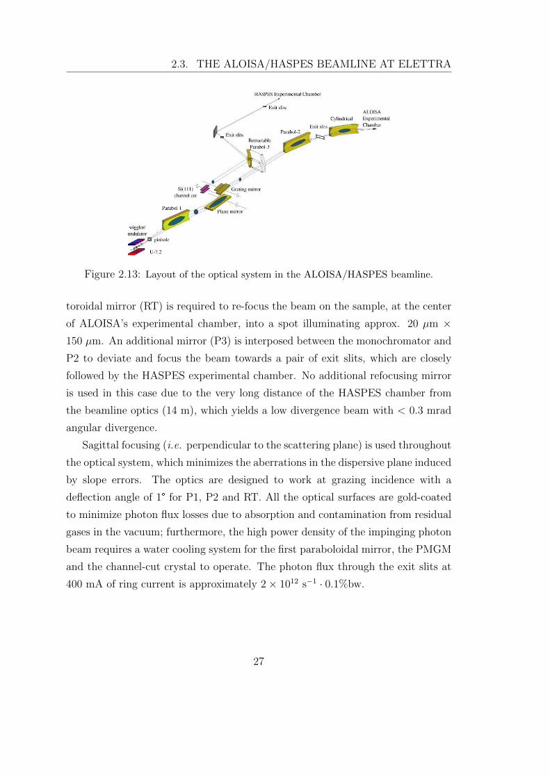
A complete layout of the optical section of the beamline is reported in Fig.
2.13. ALOISA’s monochromator covers the full 140-8000 eV range of photon en-
ergy [10]; its main characteristic is the possibility to switch between two types of
dispersing systems: a plane mirror coupled to a grating monochromator (PMGM)
or a Si(111) channel-cut crystal are employed for the low-energy (0.2-2 keV) or
high-energy (3-8 keV) range, respectively [11]. The two systems lay side by side
and they can be inserted onto the optical path by means of a sliding mechanism.
After being collected from the pinhole by a paraboloidal mirror (P1), photons are
collimated onto the dispersing system. A second paraboloidal mirror (P2) focuses
the collimated beam to the exit slits (ES) which select the photon bandwidth; a
26
2.3. THE ALOISA/HASPES BEAMLINE AT ELETTRA
Figure 2.13: Layout of the optical system in the ALOISA/HASPES beamline.
toroidal mirror (RT) is required to re-focus the beam on the sample, at the center
of ALOISA’s experimental chamber, into a spot illuminating approx. 20 µm ×150 µm. An additional mirror (P3) is interposed between the monochromator and
P2 to deviate and focus the beam towards a pair of exit slits, which are closely
followed by the HASPES experimental chamber. No additional refocusing mirror
is used in this case due to the very long distance of the HASPES chamber from
the beamline optics (14 m), which yields a low divergence beam with < 0.3 mrad
angular divergence.
Sagittal focusing (i.e. perpendicular to the scattering plane) is used throughout
the optical system, which minimizes the aberrations in the dispersive plane induced
by slope errors. The optics are designed to work at grazing incidence with a
deflection angle of 1° for P1, P2 and RT. All the optical surfaces are gold-coated
to minimize photon flux losses due to absorption and contamination from residual
gases in the vacuum; furthermore, the high power density of the impinging photon
beam requires a water cooling system for the first paraboloidal mirror, the PMGM
and the channel-cut crystal to operate. The photon flux through the exit slits at
400 mA of ring current is approximately 2× 10¹² s−1 · 0.1%bw.
27
2.3. THE ALOISA/HASPES BEAMLINE AT ELETTRA
Figure 2.14: Flux of photons at the exit of the ALOISA wiggler/undulator ID as afunction of the beam energy for selected gap values.
2.3.1 The ALOISA experimental chamber
Fig. 2.15 (A) schematically illustrates the setup of the ALOISA chamber. A
hemispherical void, dedicated to the sample preparation (preparation chamber), is
separated by a vacuum valve from a cylindrical void hosting the electron analyzers
and photon detector for sample investigations (main chamber). The two parts are
coupled via a large ball bearing and a system of sliding O-rings, which, with the
introduction of two differential pumping stages, allow the complete rotation of the
main chamber around the synchrotron beam axis keeping a base pressure of 10−11
mbar, while the preparation chamber remains still.
The preparation chamber is equipped with a MBE (Molecular Beam
Epitaxy) cryopanel which can host up to four evaporation cells; two quartz
microbalances are used to monitor the particle flux during an evaporation.
A gas line enables the flow of high purity gases into the chamber. Sample
cleaning is usually performed with Ar+ sputtering at an ion energy of up to
3 keV. A RHEED gun (Reflection High Energy Electron Diffraction) with
electron energy of 15 keV sends an electron beam at grazing incidence onto
28
2.3. THE ALOISA/HASPES BEAMLINE AT ELETTRA
the sample surface to determine the surface symmetry or check in situ the
order of a molecular layer during deposition. An extraction and a transfer
arm, coupled to a fast-entry load-lock system, allow a quick sample exchange.
Figure 2.15: Schematic diagrams of (A) ALOISA and (B) HASPES experimental cham-ber.
In the main chamber, the detectors are hosted on two frames which are
mounted inside the rotating element. The axial frame is mounted at the end
of the cylindrical element and can rotate around the synchrotron beam axis
independently of the chamber (see 2.17 (B)). Five 33 mm electron analyzers are
mounted on this frame, which are primarily dedicated for the APECS (Auger
Photoelectron Coincidence Spectroscopy). A phosphorous plate with a CCD
camera is also mounted on the axial frame for beam alignment purpose. The
bimodal frame is inserted into a side of the main chamber cylinder; it can rotate
around an axis perpendicular to the synchrotron beam. The bimodal frame
29
2.3. THE ALOISA/HASPES BEAMLINE AT ELETTRA
moves integrally with the main chamber around the synchrotron beam axis. A
66 mm hemispherical electron analyzer is found in its interior for angle-resolved
photoemission (ARPES) and photoelectron diffraction (PED) measurements.
There is one Si-diode behind 1 mm collimators for measuring the total current for
X-ray diffraction (XRD) and reflectivity (XRR). The bimodal frame additionally
hosts one energy-resolved (Peltier-cooled) photodiode (by Eurisis) operating in
single-photon counting mode for X-ray diffraction. The partial electron yield
(PEY) mode for measuring the NEXAFS signal employs a wide-angle acceptance
channeltron mounted on the axis of the bimodal frame. The low-energy multiple-
scattered electrons are repelled by a grid polarized with an adjustable negative
potential, placed at the channeltron apex, so as to improve the surface sensitivity
and signal-to-noise ratio by collecting the high-energy Auger electrons only.
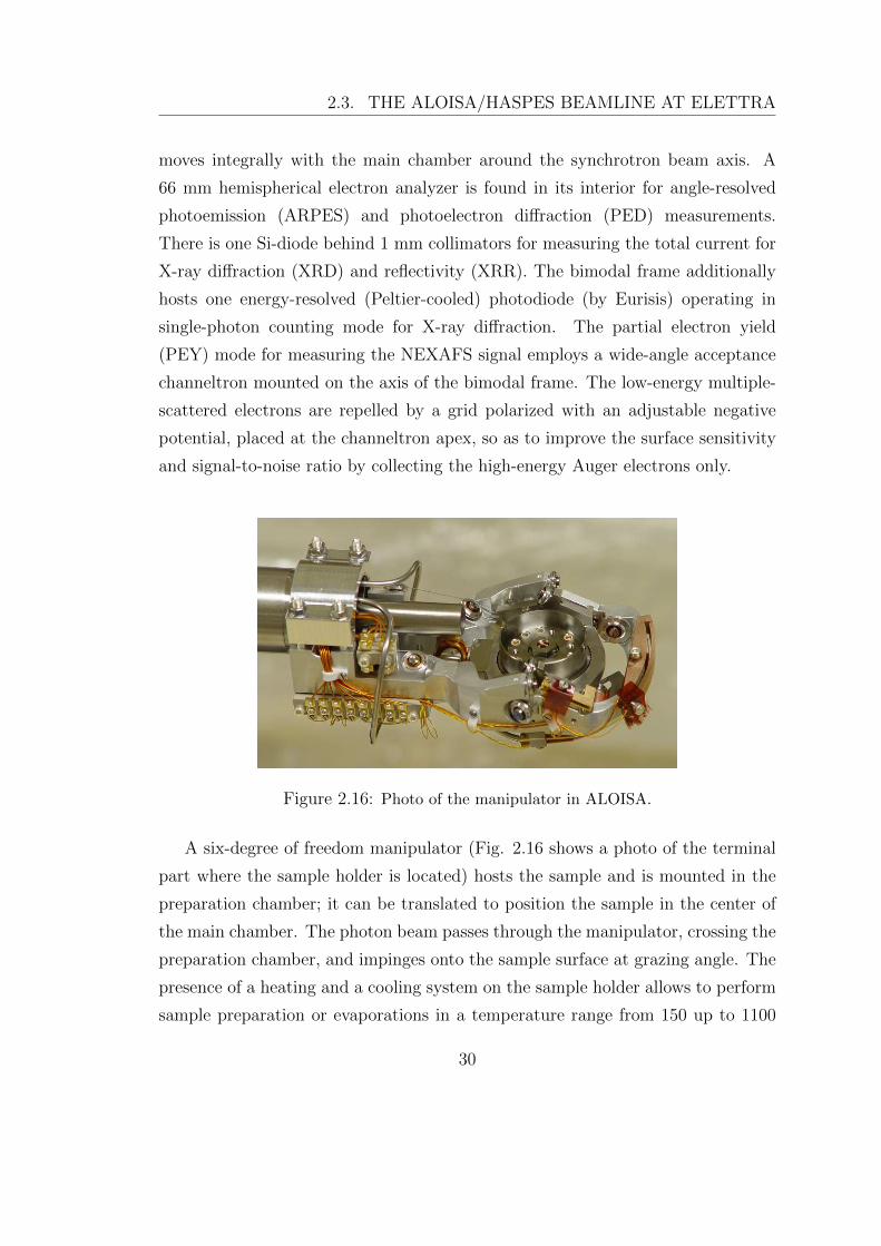
Figure 2.16: Photo of the manipulator in ALOISA.
A six-degree of freedom manipulator (Fig. 2.16 shows a photo of the terminal
part where the sample holder is located) hosts the sample and is mounted in the
preparation chamber; it can be translated to position the sample in the center of
the main chamber. The photon beam passes through the manipulator, crossing the
preparation chamber, and impinges onto the sample surface at grazing angle. The
presence of a heating and a cooling system on the sample holder allows to perform
sample preparation or evaporations in a temperature range from 150 up to 1100
30
2.3. THE ALOISA/HASPES BEAMLINE AT ELETTRA
K. The heat is provided by two tungsten filaments; a high voltage can be applied
to the sample holder for electron bombardment. The cooling system consists of
a pipeline where flowing nitrogen is brought to its liquefaction temperature at
atmospheric pressure (77 K); a copper finger acts as thermal contact bridging the
pipeline with the sample holder.
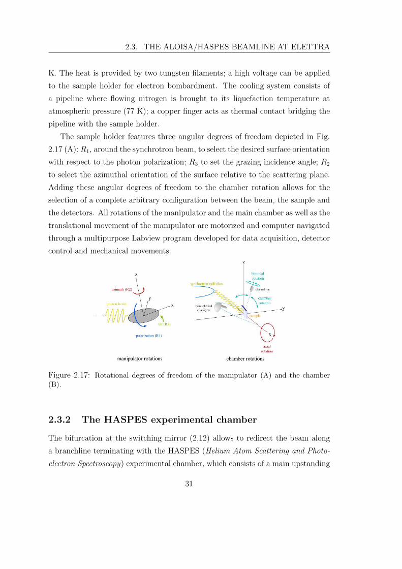
The sample holder features three angular degrees of freedom depicted in Fig.
2.17 (A): R1, around the synchrotron beam, to select the desired surface orientation
with respect to the photon polarization; R3 to set the grazing incidence angle; R2
to select the azimuthal orientation of the surface relative to the scattering plane.
Adding these angular degrees of freedom to the chamber rotation allows for the
selection of a complete arbitrary configuration between the beam, the sample and
the detectors. All rotations of the manipulator and the main chamber as well as the
translational movement of the manipulator are motorized and computer navigated
through a multipurpose Labview program developed for data acquisition, detector
control and mechanical movements.
Figure 2.17: Rotational degrees of freedom of the manipulator (A) and the chamber(B).
2.3.2 The HASPES experimental chamber
The bifurcation at the switching mirror (2.12) allows to redirect the beam along
a branchline terminating with the HASPES (Helium Atom Scattering and Photo-
electron Spectroscopy) experimental chamber, which consists of a main upstanding
31
2.3. THE ALOISA/HASPES BEAMLINE AT ELETTRA
cylindrical void, a pre-chamber hosting a He atom source, and a chamber enclosing
the quadrupole mass spectrometer for He atom detection. A top view scheme is
reported in Fig. 2.15 (B).
The HASPES line is dedicated to the combined use of soft X-rays in the energy
range 120-1000 eV, ultraviolet He I photoemission (21.2 eV) and He atom scatter-
ing. He atom scattering is a truly surface sensitive and non-destructive technique
enabling the investigation of the outermost surface charge density corrugation. A
collimated beam of thermal He atoms (energy ∼ 26 meV) cannot penetrate nor
damage the first surface layer because of its low energy: it is scattered by exchang-
ing momentum with the surface electron density. The elastically diffracted He
atoms are subsequently ionized and selected by a quadrupole mass spectrometer.
The whole diffraction pattern can be mapped out through the rotational movement
of the sample about the axis of R1. The combination of this technique with the
chemical sensitivity of electron spectroscopies offers the advantage of probing in
situ and simultaneously the growth mode, ordering and chemistry of self-assembled
monolayers.
The vacuum line where the photon beam travels is connected to the quadrupole
detection system, so that the photons enter the HASPES chamber in a direction
opposite to the scattered He atoms. The main chamber has a VG CTPO manipu-
lator vertically inserted, with six degrees of freedom and high-precision positioning.
A fixed scattering geometry is adopted with a source-sample-detector angle of 110°
for HAS and 55° for XPS, as represented in Fig. 2.15 (B). The three angular de-
grees of freedom for the manipulator are R1, which changes the incidence angle
of He atoms and the synchrotron beam; R2, which varies the orientation of the
surface symmetry axis with respect to the scattering plane; R3, which tilts the
sample about a horizontal axis. All the manipulator rotations are motorized and
controlled via a home-made Labview program, which also manages the data ac-
quisition. A thermal link connecting the manipulator base to a liquid-N cryostat,
and a tungsten filament or resistive heating in the rear side allow to work with the
surface in the 150-1100 K temperature interval.
A differentially pumped He lamp is also attached to the main chamber, pro-
32
2.3. THE ALOISA/HASPES BEAMLINE AT ELETTRA
viding ultraviolet He I photons for the characterization of valence band states.
The low photon energy enhances the absorption cross section of shallow electronic
states, which, in combination with a 150 mm hemispherical electron analyzer, al-
lows for the measurement of high resolution valence band in thin films. The latter
hosts a 2D delay-line anode behind two serially coupled multichannel plates (MCP)
and offers an energy resolution of 0.5% of the pass energy, with a 17 meV upper
bound limit. Additionally, a channeltron is mounted at an angle of 50° from above
the horizontal scattering plane for the PEY detection of NEXAFS electrons. An
ion gun for Ar+ sputtering and a liquid-N cooled cryopanel hosting three evapora-
tion cells offer a complete set of tools for sample cleaning and MBE. Finally, the
chamber is endowed with a load-lock system for sample exchange.
33
2.4. REFERENCES (CH. 2)
2.4 References (Ch. 2)
[1] C Julian Chen. Introduction
to scanning tunneling microscopy,
volume 227. Oxford University
Press New York, 1993.
[2] J. Bardeen. Tunnelling from a
many-particle point of view. Phys.
Rev. Lett., 6:57–59, Jan 1961.
[3] J Tersoff and DR Hamann. The-
ory of the scanning tunneling mi-
croscope. In Scanning Tunneling
Microscopy, pages 59–67. Springer,
1993.
[4] LEC Van de Leemput and
H Van Kempen. Scanning
tunnelling microscopy. Reports on
Progress in Physics, 55(8):1165,
1992.
[5] Friedrich Reinert and Stefan
Hufner. Photoemission spec-
troscopy - from early days to
recent applications. New Journal
of Physics, 7(1):97, 2005.
[6] Stefan Hufner. Photoelectron spec-
troscopy: principles and applica-
tions. Springer, 2003.
[7] Jens Als-Nielsen and Des McMor-
row. Elements of modern X-ray
physics. John Wiley & Sons, 2011.
[8] Georg Hahner. Near edge X-
ray absorption fine structure spec-
troscopy as a tool to probe elec-
tronic and structural properties
of thin organic films and liq-
uids. Chemical Society Reviews,
35(12):1244–1255, 2006.
[9] Joachim Stohr. NEXAFS spec-
troscopy, volume 25. Springer,
1992.
[10] L Floreano, G Naletto, D Cvetko,
R Gotter, M Malvezzi, L Marassi,
A Morgante, A Santaniello, A Ver-
dini, F Tommasini, et al. Per-
formance of the grating-crystal
monochromator of the aloisa beam-
line at the elettra synchrotron.
Review of scientific instruments,
70(10):3855–3864, 1999.
[11] E Busetto, A Lausi, and S Bern-
storff. The high-energy monochro-
mator for the aloisa beamline at
elettra. Review of scientific instru-
ments, 66(2):2078–2081, 1995.
34
3 Titanium dioxide
and its Rutile (110) surface
3.1 Titanium dioxide
Research on metal oxides is emerging as a new, rapidly growing area in surface
science due to the interesting chemical and physical properties of these materi-
als, and the need of modeling more realistic systems, since nearly every metal
surface is readily oxidized in air. Titanium dioxide, TiO2, a member of the tran-
sition metal oxide family, is one of the most intensively studied oxide materials
thanks to the technological applications disclosed by its properties. It is found in
nature in three polymorphs: Anatase, Rutile and Brookite. Anatase and Rutile
are by far the most important phases from the point of view of both technology
and science. They are semiconductors with a similar energy gap (3.2 and 3.0
eV, respectively), which matches the HOMO-LUMO gap of many light-harvesting
compounds (dyes). Synthetic chemistry routes allow the functionalization of dyes
to provide them with anchoring groups to bind to TiO2 surfaces, which, along
with the capability of growing TiO2 nanostructures with a very large surface to
volume ratio (i.e. nanocrystallites or hollow nanowires, see Fig. 3.1), is key to
one of the applications capable of potentially reshaping the way energy is pro-
duced in our societies: dye-sensitized solar cells [1]. Other important applications
of TiO2 make use of its chemically active crystal facets, such as Anatase-(101) or
Rutile-(110), which, upon thermal treatment, exhibit high concentrations of free
carriers (electrons). Photocatalytic activity is achieved when these surfaces are
illuminated with ultraviolet light: toxic organic molecules and impurities are then
35
3.1. TITANIUM DIOXIDE
split into simpler compounds, such as carbon dioxide. The process is exploited
for the production of self-cleaning glasses, water-splitting or bactericidal surfaces
[2]. One can also take advantage of TiO2 high dielectric constant by building top-
contact thin film transistors where the drain current is tuned by a voltage applied
to a TiO2 gate layer. The high surface corrugation available in some TiO2 sur-
faces, such as Rutile-(110), could yield a superior templated growth of the organic
molecules employed as semiconductors for the transisitor active channel, increasing
their electron mobility.
Figure 3.1: Scanning electron microscope images providing an example of the versatilityof TiO2 as a material for nanostructured coatings: close view of TiO2 (A) nanospheres(after [7]), and (B) hollow nanotubes (after [8]). The high surface to volume ratio isessential in dye-sensitized solar cells to maximize the light harvested by the dye/TiO2
coating.
Mesoporous TiO2 layers in prototypical dye-sensitized solar cells usually consist
of a mixture of Anatase and Rutile crystals, with the former highly predominant,
which is beneficial for the device efficiency. The presence of electron trap states in
Rutile, independently of the type of nanostructures (nanoparticles or nanowires),
is arguably responsible for enhanced charge recombination in the semiconductor,
before the carriers reach the metallic lead, resulting in a lower photogenerated
36
3.2. THE RUTILE (110)-1×1 SURFACE
current [3]. However, Rutile offers a suitable playground to model the adsorption of
organic molecules, since it is commercially available in the form of cut and polished
single-crystals exposing the desired crystal facet. In particular, its (110) surface has
been subject to extensive characterization, becoming the archetypal metal oxide
surface: its structure and geometry have been solved, furthermore, the preparation
procedure of a clean surface is straightforward. In the following, a short overview
of the Rutile-(110) surface will be given, including its reduced 1×2 reconstruction.
Figure 3.2: Ball-and-stick models of Rutile (left) and Anatase (right) unit cell. Sym-metry group, axis lengths and angles are reported. In both structures, each Ti atom issurrounded by 6 oxygen atoms located at the vertices of an octahedron.
3.2 The Rutile (110)-1×1 surface
The Rutile polymorph is the most stable crystal phase of TiO2. Its unit cell,
reported in Fig. 3.2, belongs to the body-centered tetragonal group, and features
a Ti ion, with formal charge +4, immersed in an octahedral environment where
it is coordinated to six O ions of formal charge -2. Each O ion is placed at one
vertex of the octahedron. Bulk Ti and O ions have thus a coordination number of
6 and 3, respectively. The Rutile-(110) surface derives from the simple truncation
of the bulk crystal across its (110) plane, as indicated in Fig. 3.3 by the yellow
37
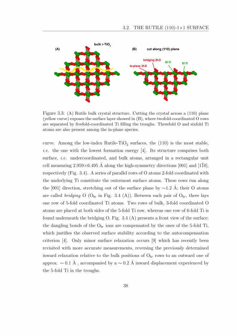
3.2. THE RUTILE (110)-1×1 SURFACE
Figure 3.3: (A) Rutile bulk crystal structure. Cutting the crystal across a (110) plane(yellow curve) exposes the surface layer showed in (B), where twofold-coordinated O rowsare separated by fivefold-coordinated Ti filling the troughs. Threefold O and sixfold Tiatoms are also present among the in-plane species.
curve. Among the low-index Rutile-TiO2 surfaces, the (110) is the most stable,
i.e. the one with the lowest formation energy [4]. Its structure comprises both
surface, i.e. undercoordinated, and bulk atoms, arranged in a rectangular unit
cell measuring 2.959×6.495 A along the high-symmetry directions [001] and [110],
respectively (Fig. 3.4). A series of parallel rows of O atoms 2-fold coordinated with
the underlying Ti constitute the outermost surface atoms. These rows run along
the [001] direction, stretching out of the surface plane by ∼1.2 A; their O atoms
are called bridging O (Obr in Fig. 3.4 (A)). Between each pair of Obr, there lays
one row of 5-fold coordinated Ti atoms. Two rows of bulk, 3-fold coordinated O
atoms are placed at both sides of the 5-fold Ti row, whereas one row of 6-fold Ti is
found underneath the bridging O. Fig. 3.4 (A) presents a front view of the surface:
the dangling bonds of the Obr ions are compensated by the ones of the 5-fold Ti,
which justifies the observed surface stability according to the autocompensation
criterion [4]. Only minor surface relaxation occurs [9] which has recently been
revisited with more accurate measurements, reversing the previously determined
inward relaxation relative to the bulk positions of Obr rows to an outward one of
approx. ∼ 0.1 A , accompanied by a ∼ 0.2 A inward displacement experienced by
the 5-fold Ti in the troughs.
38
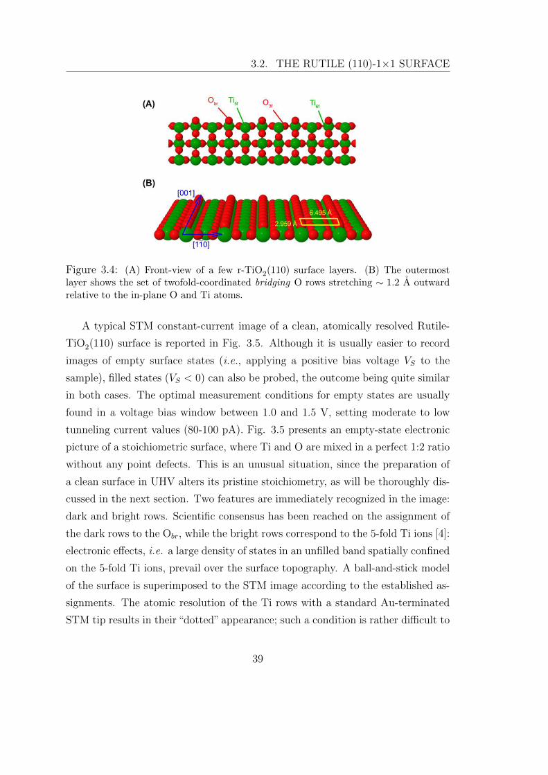
3.2. THE RUTILE (110)-1×1 SURFACE
Figure 3.4: (A) Front-view of a few r-TiO2(110) surface layers. (B) The outermostlayer shows the set of twofold-coordinated bridging O rows stretching ∼ 1.2 A outwardrelative to the in-plane O and Ti atoms.
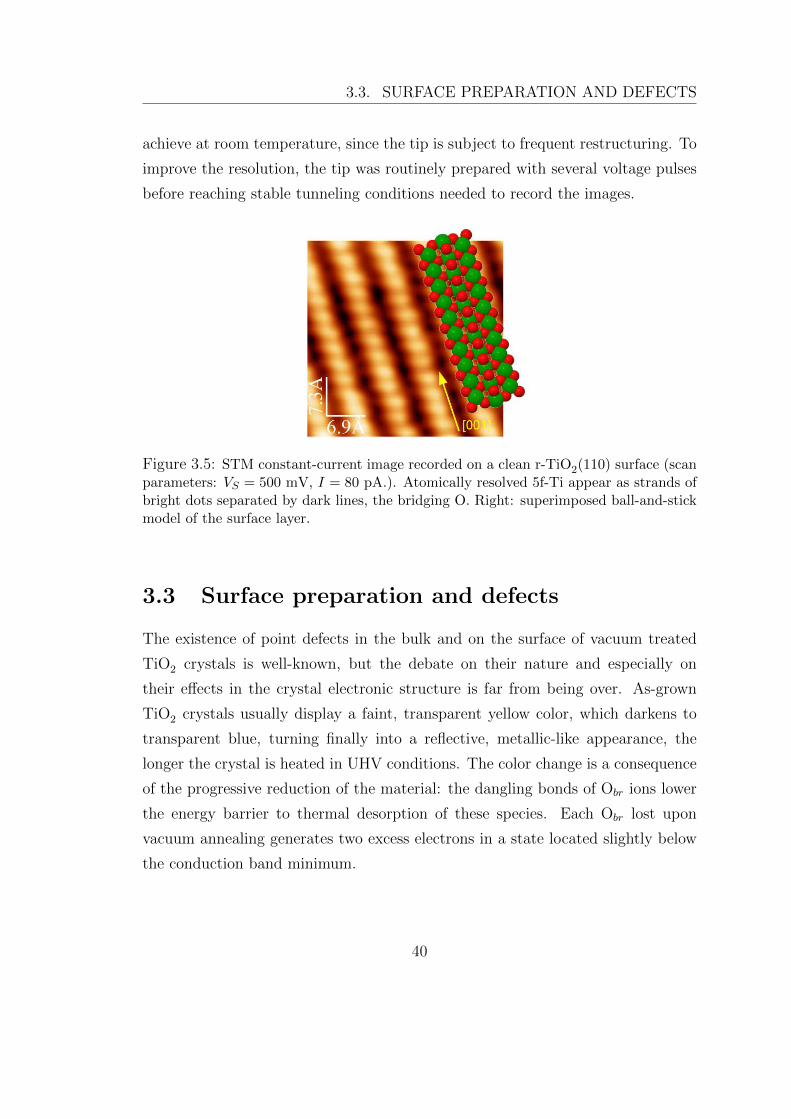
A typical STM constant-current image of a clean, atomically resolved Rutile-
TiO2(110) surface is reported in Fig. 3.5. Although it is usually easier to record
images of empty surface states (i.e., applying a positive bias voltage VS to the
sample), filled states (VS < 0) can also be probed, the outcome being quite similar
in both cases. The optimal measurement conditions for empty states are usually
found in a voltage bias window between 1.0 and 1.5 V, setting moderate to low
tunneling current values (80-100 pA). Fig. 3.5 presents an empty-state electronic
picture of a stoichiometric surface, where Ti and O are mixed in a perfect 1:2 ratio
without any point defects. This is an unusual situation, since the preparation of
a clean surface in UHV alters its pristine stoichiometry, as will be thoroughly dis-
cussed in the next section. Two features are immediately recognized in the image:
dark and bright rows. Scientific consensus has been reached on the assignment of
the dark rows to the Obr, while the bright rows correspond to the 5-fold Ti ions [4]:
electronic effects, i.e. a large density of states in an unfilled band spatially confined
on the 5-fold Ti ions, prevail over the surface topography. A ball-and-stick model
of the surface is superimposed to the STM image according to the established as-
signments. The atomic resolution of the Ti rows with a standard Au-terminated
STM tip results in their “dotted” appearance; such a condition is rather difficult to
39
3.3. SURFACE PREPARATION AND DEFECTS
achieve at room temperature, since the tip is subject to frequent restructuring. To
improve the resolution, the tip was routinely prepared with several voltage pulses
before reaching stable tunneling conditions needed to record the images.
Figure 3.5: STM constant-current image recorded on a clean r-TiO2(110) surface (scanparameters: VS = 500 mV, I = 80 pA.). Atomically resolved 5f-Ti appear as strands ofbright dots separated by dark lines, the bridging O. Right: superimposed ball-and-stickmodel of the surface layer.
3.3 Surface preparation and defects
The existence of point defects in the bulk and on the surface of vacuum treated
TiO2 crystals is well-known, but the debate on their nature and especially on
their effects in the crystal electronic structure is far from being over. As-grown
TiO2 crystals usually display a faint, transparent yellow color, which darkens to
transparent blue, turning finally into a reflective, metallic-like appearance, the
longer the crystal is heated in UHV conditions. The color change is a consequence
of the progressive reduction of the material: the dangling bonds of Obr ions lower
the energy barrier to thermal desorption of these species. Each Obr lost upon
vacuum annealing generates two excess electrons in a state located slightly below
the conduction band minimum.
40
3.3. SURFACE PREPARATION AND DEFECTS
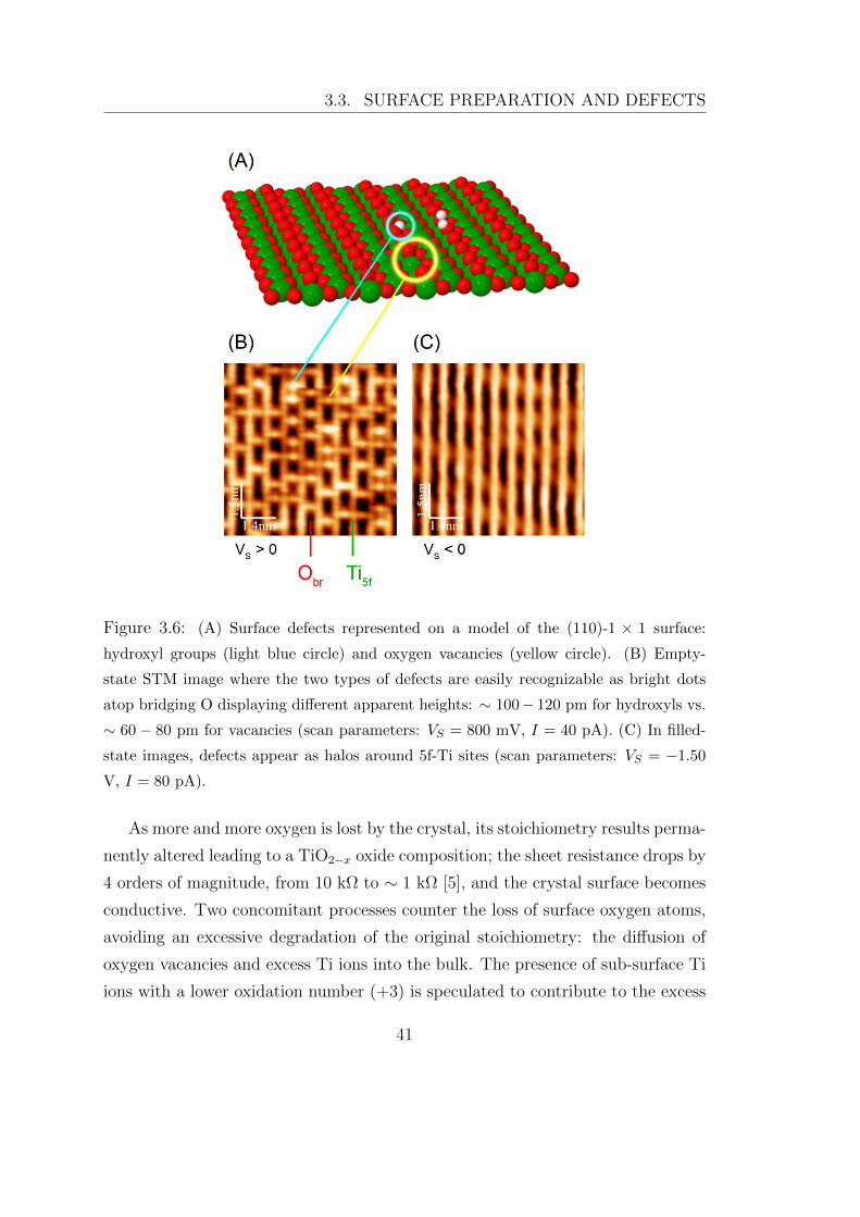
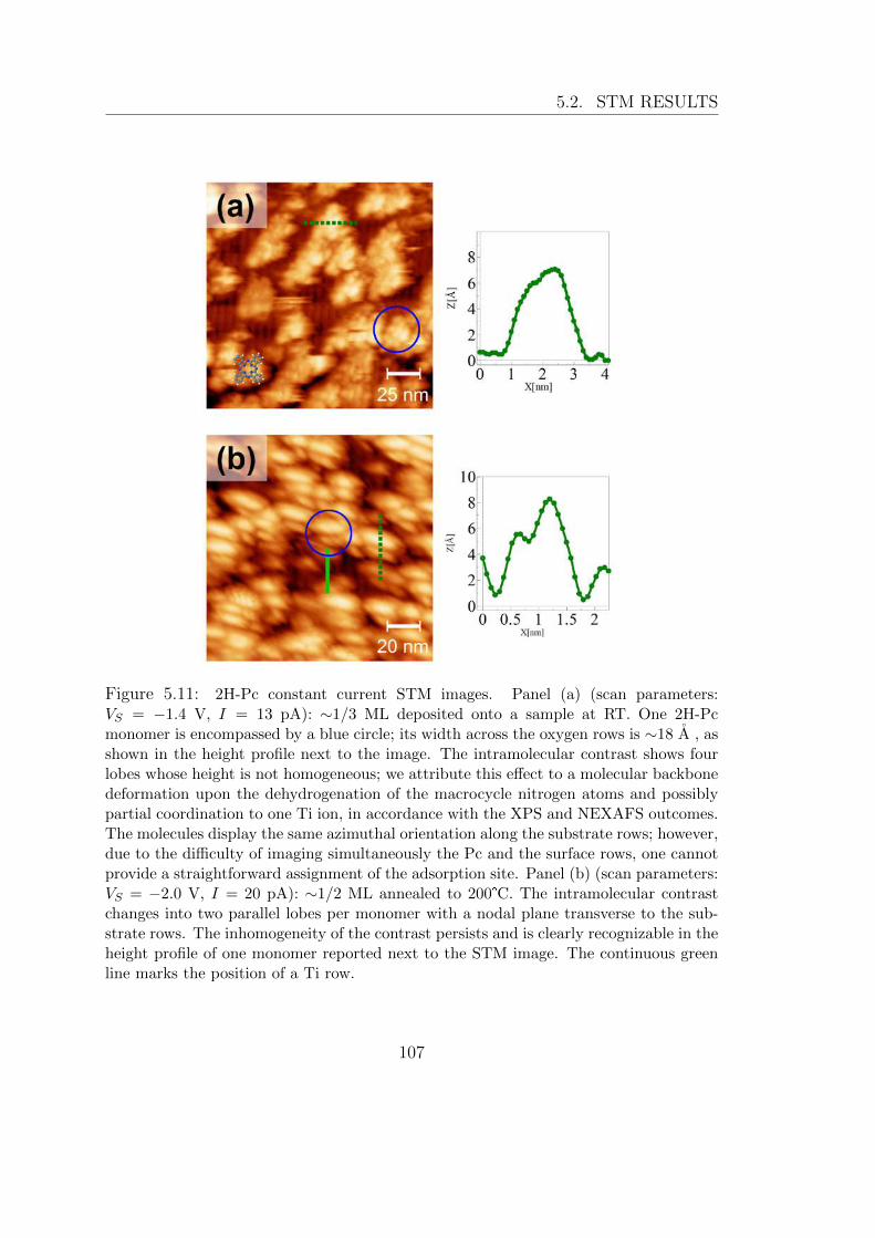
Figure 3.6: (A) Surface defects represented on a model of the (110)-1 × 1 surface:
hydroxyl groups (light blue circle) and oxygen vacancies (yellow circle). (B) Empty-
state STM image where the two types of defects are easily recognizable as bright dots
atop bridging O displaying different apparent heights: ∼ 100− 120 pm for hydroxyls vs.
∼ 60− 80 pm for vacancies (scan parameters: VS = 800 mV, I = 40 pA). (C) In filled-
state images, defects appear as halos around 5f-Ti sites (scan parameters: VS = −1.50
V, I = 80 pA).
As more and more oxygen is lost by the crystal, its stoichiometry results perma-
nently altered leading to a TiO2−x oxide composition; the sheet resistance drops by
4 orders of magnitude, from 10 kΩ to ∼ 1 kΩ [5], and the crystal surface becomes
conductive. Two concomitant processes counter the loss of surface oxygen atoms,
avoiding an excessive degradation of the original stoichiometry: the diffusion of
oxygen vacancies and excess Ti ions into the bulk. The presence of sub-surface Ti
ions with a lower oxidation number (+3) is speculated to contribute to the excess
41
3.3. SURFACE PREPARATION AND DEFECTS
charge available in reduced TiO2 crystals, and to influence the observed catalytic
activity [6], although there is no broad consensus on the matter.
The preparation procedure adopted to get a clean surface is made up of two
steps:
15-30 minutes of Ar+ sputtering at typically 1.0 keV ion energy and 10−6
mbar Ar pressure, to remove a few surface layers.
A subsequent annealing cycle to restore the (1× 1) structure, accomplished
by electron bombardment. A voltage of 800 V is supplied to the sample,
while the emission current is stabilized at 10 mA for 4 minutes, 20 mA for 2
minutes and finally 40-50 mA for 1 minute.
The annealing temperature during the last step reaches 750°C; the loss of oxygen
makes the sample conductive enough to be probed with photoelectron spectro-
scopies and STM avoiding charging effects, but it also increases the density of
surface and sub-surface defects which may condition the adsorption of molecules.
The pair of excess electrons released in Rutile-TiO2(110) upon the formation of
one oxygen vacancy (Ovac) redistribute over some surface and sub-surface Ti sites
[10]. Although Ovac are thought of making up a large part of point defects on a
TiO2 surface in good vacuum conditions, a water-splitting reaction at the vacancy
sites on the surface is responsible for the conversion of on-surface vacancies into
hydroxyl groups, i.e. hydrogen-capped Obr atoms, when the sample is exposed to
water vapors or simply because of the residual water in the vacuum. Some recent
studies suggest that even a perfect TiO2 surface is capable of splitting adsorbed
water molecules at room temperature [11]. The dissociation of one water molecule
at a vacancy site generates two hydroxyl groups. Both types of defects, oxygen
vacancies and hydroxyls, are readily recognizable in an empty-state STM image,
as the one reported in Fig. 3.6 (B). Ovac appear as scattered bright “bridges”,
each occupying one Obr sites and connecting two adjacent 5-fold Ti rows; OH
groups share the same appearance and position of Ovac, but their STM height is
approximately double. Notably, the defect contrast changes when the bias voltage
is switched from positive to negative [12] in Fig. 3.6 (C) (where the image has
42
3.3. SURFACE PREPARATION AND DEFECTS
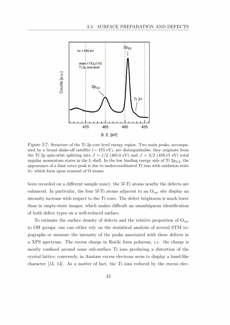
Figure 3.7: Structure of the Ti 2p core level energy region. Two main peaks, accompa-nied by a broad shake-off satellite (∼ 473 eV), are distinguishable; they originate fromthe Ti 2p spin-orbit splitting into J = 1/2 (465.0 eV) and J = 3/2 (459.15 eV) totalangular momentum states in the L shell. In the low binding energy side of Ti 2p3/2, theappearance of a faint extra peak is due to undercoordinated Ti ions with oxidation state3+ which form upon removal of O atoms.
been recorded on a different sample zone): the 5f-Ti atoms nearby the defects are
enhanced. In particular, the four 5f-Ti atoms adjacent to an Ovac site display an
intensity increase with respect to the Ti rows. The defect brightness is much lower
than in empty-state images, which makes difficult an unambiguous identification
of both defect types on a well-reduced surface.
To estimate the surface density of defects and the relative proportion of Ovac
to OH groups, one can either rely on the statistical analysis of several STM to-
pographs or measure the intensity of the peaks associated with these defects in
a XPS spectrum. The excess charge in Rutile form polarons, i.e. the charge is
mostly confined around some sub-surface Ti ions producing a distortion of the
crystal lattice; conversely, in Anatase excess electrons seem to display a band-like
character [13, 14]. As a matter of fact, the Ti ions reduced by the excess elec-
43
3.3. SURFACE PREPARATION AND DEFECTS
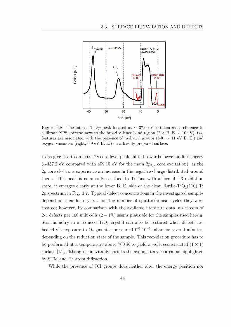
Figure 3.8: The intense Ti 3p peak located at ∼ 37.6 eV is taken as a reference tocalibrate XPS spectra; next to the broad valence band region (2 < B. E. < 10 eV), twofeatures are associated with the presence of hydroxyl groups (left, ∼ 11 eV B. E.) andoxygen vacancies (right, 0.9 eV B. E.) on a freshly prepared surface.
trons give rise to an extra 2p core level peak shifted towards lower binding energy
(∼457.2 eV compared with 459.15 eV for the main 2p3/2 core excitation), as the
2p core electrons experience an increase in the negative charge distributed around
them. This peak is commonly ascribed to Ti ions with a formal +3 oxidation
state; it emerges clearly at the lower B. E. side of the clean Rutile-TiO2(110) Ti
2p spectrum in Fig. 3.7. Typical defect concentrations in the investigated samples
depend on their history, i.e. on the number of sputter/anneal cycles they were
treated; however, by comparison with the available literature data, an esteem of
2-4 defects per 100 unit cells (2− 4%) seems plausible for the samples used herein.
Stoichiometry in a reduced TiO2 crystal can also be restored when defects are
healed via exposure to O2 gas at a pressure 10−6-10−5 mbar for several minutes,
depending on the reduction state of the sample. This reoxidation procedure has to
be performed at a temperature above 700 K to yield a well-reconstructed (1 × 1)
surface [15], although it inevitably shrinks the average terrace area, as highlighted
by STM and He atom diffraction.
While the presence of OH groups does neither alter the energy position nor
44
3.3. SURFACE PREPARATION AND DEFECTS
quench the Ti3+ peak, two other important electronic signatures of defect electrons
are found in the valence band spectrum, reported in Fig. 3.8, which allow for the
discrimination between Ovac and OH groups. At ∼ −0.9 eV binding energy it is
located the first peak (magnified 10 times in the red inset) associated with defect
electrons. Whenever some charge is statically transferred to the TiO2 surface, be it
via oxygen vacancy creation or adsorption of electron-donating atoms or molecules,
excess electrons fill this trap state and appear to be localized around the same sites
[10]. The replacement of Ovac with hydroxyls happens quickly enough to saturate
the surface vacancies in 10-20 minutes, as soon as the freshly annealed surface
begins to cool down. The process does not quench the defect peak [16]; instead, a
new feature is observed at a binding energy of ∼ 11 eV, left of the broad valence
band profile in Fig. 3.8. Hydroxyl groups are easily cleaved via exposure to 5-30
L of O2 at room temperature; the exposure has to be calibrated to the effective
defect concentration in order to minimize the formation of adsorbed O atoms from
the dissociation of O2 molecules on the 5-fold Ti rows, which may affect the surface
properties. Therefore, surfaces with the desired defect density, prepared by thermal
annealing or carefully calibrated O2 exposure, allow to assess the effects of Ovac or
OH groups on the adsorption of organic molecules.
3.3.1 The Rutile (110)-1×2 surface
A TiO2(110) crystal can be strongly reduced by a long annealing; the sample be-
comes dark blue and the Ovac surface density approaches an upper limit of about
8−10%. Prolonged reduction triggers a surface reconstruction into a (1×2) struc-
ture: the periodicity of the pristine TiO2(110) doubles across the surface rows.
The reconstruction proceeds via the formation of oxygen-deficient strands, grow-
ing over 5-fold Ti rows until a complete (1× 2) terrace has formed [18]. There has
been considerable debate on the precise composition of the reconstructed layer,
with several proposed models. Recently, an accurate LEED-IV study [17] demon-
strated that the correct surface geometry for a simple, defect-free, TiO2(110)(1×2)
reconstruction was predicted by Onishi and Iwasawa [19]: it is the Ti2O3 added-
row model illustrated in Fig. 3.9 (A). One Ti2O3 row, made up of three O and
45
3.3. SURFACE PREPARATION AND DEFECTS
Figure 3.9: (A) Ball-and-stick model of a 1 × 2, defect-free reconstructed r-TiO2(110)surface. It represents the model first proposed by Onishi and Iwasawa, where a Ti2O3
row is added on top of every bridging oxygen row. The horizontal periodicity thusdoubles (13 A). (B) STM constant-current image recorded on a strongly reduced TiO2
sample: 1×1 terraces (bottom) host numerous bright strands, which precede the growthof 1× 2 layers (top) (scan parameters: VS = 900 mV, I = 80 pA.
46
3.4. ADSORPTION OF ORGANIC MOLECULES ON RUTILE-(110)
two Ti ions per one unit cell length along the [001] direction, is added on top of a
5-fold Ti row every two Obr rows.
Below Fig. 3.9 (A), the STM constant-current image of a partially recon-
structed sample shows the presence of two distinct areas. The first half of the
image hosts a (1×2) reconstructed terrace with scattered point defects, which can
be directly compared with the stranded appearance of a (1× 1) terrace still in the
process of conversion into the (1× 2) structure.
The homogeneity of the reconstructed rows is perturbed by the presence of
point defects which tend to aggregate into linear chains. These defects are classified
into single links or cross links according to their shape and size; the occurrence of
the so-called cross-linked reconstruction they originate depends on the extent of
the crystal bulk reduction[20]: it is commonly observed in deeply reduced samples.
The exact structure of this reconstruction is still disputed; a model based on Ti3O6
oxygen-rich rows is backed by recent non-contact AFM measurements [21], but to
date no quantitative studies on the cross-linked reconstruction are available.
3.4 Adsorption of organic molecules
on Rutile-(110)
The research on TiO2-organic interfaces has considerably expanded in recent
years. Dye-sensitized solar cells (DSSC) [22] and organic thin-film transistors
[23] have been fabricated with a variety of organic molecules; however, poor
knowledge of the properties of TiO2-organic interfaces is one of the factors limiting
the efficiency of these devices. The importance of the TiO2(110) surface as a
model system to gain insight into the chemistry of organodielectric interfaces
was made clear by several ground-breaking studies on the nature and role of
TiO2 defects in processes such as the reoxidation of a reduced crystal or the
splitting of adsorbed water molecules. Besides the defect chemistry, recent work
focused on the correlation between chemical interactions and fast charge injection
into the conduction band of the crystal from photoexcited species, employed
in highly efficient metallorganic light-harvesting complexes [24, 25, 26, 27].
47
3.4. ADSORPTION OF ORGANIC MOLECULES ON RUTILE-(110)
Resonant photoemission measurements established an upper bound for dynamic
charge transfer as low as 10-20 fs for a Ruthenium-based dye, and < 3 fs
for one of its ligands, bi-isonicotinic acid. As elucidated by XPS, for both
molecules the bonding to the surface takes place with a deprotonation of the
carboxylic moieties as they adsorb vertically on the 5-fold Ti troughs. This
result sparked fresh research with the aim of finding stable linker groups to the
surface, while simultaneously keeping the empty energy levels of the adsorbate
above the TiO2 conduction band to maximize the probability of charge transfer.
Organic molecules appended with a variety of terminations were characterized on
r-TiO2(110): alcohols and aldehydes [28], amines [29], azo-terminated compounds
[30], pyridines [31], phosphonated compounds [32], aromatic hydrocarbons [4], etc.
Table 3.1: Parameters needed for the vacuum purification and deposition of the selected
organic molecules.
The bidentate adsorption of carboxylic-terminated molecules also yielded the first
successful attempts to functionalize a metal oxide surface through the formation
of ordered self-assembled layers [34, 35]. Interestingly, the suppression of surface
defects could be achieved chemically through the adsorption of a functionalized
pyridine compound exhibiting a specific affinity towards oxygen vacancies [36].
48
3.4. ADSORPTION OF ORGANIC MOLECULES ON RUTILE-(110)
An electron transfer from the reduced Ti+3 ions to the pyridines bound at the
vacancy sites determined a nearly complete quenching of the defect state peak,
which suggests that the surface excess charge is predominantly Ovac-derived, at
least for moderately reduced samples.
Two subgroups of conjugated organic compounds deserve special considera-
tion because of their importance in organic-based technologies: a) acenes and
functionalized perylenes, molecules displaying large free carrier mobilities; and b)
metallorganic dyes derived from phthalocyanines and porphyrins, which have been
shown to reach photoconversion efficiencies comparable or higher than the best
transition metal complexes based on rare-earth ions (> 13%) [37]. In an attempt
to broaden the available knowledge on these technologically important organics,
the present work investigates the adsorption on r-TiO2(110) of the species listed
in Tab. 3.1 along with some useful experimental data.
49
3.5. REFERENCES (CH. 3)
3.5 References (Ch. 3)
[1] Brian O’Regan and Michael
Gratzel. A low-cost, high-efficiency
solar cell based on dye-sensitized
colloidal TiO2 films. Nature,
353(6346):737–740, 1991.
[2] Kazuhito Hashimoto, Hiroshi Irie,
and Akira Fujishima. TiO2 photo-
catalysis: a historical overview and
future prospects. Japanese journal
of applied physics, 44(12R):8269,
2005.
[3] Emil Enache-Pommer, Bin Liu,
and Eray S Aydil. Electron
transport and recombination in
dye-sensitized solar cells made
from single-crystal rutile TiO2
nanowires. Physical Chemistry
Chemical Physics, 11(42):9648–
9652, 2009.
[4] Ulrike Diebold. The surface science
of titanium dioxide. Surface science
reports, 48(5):53–229, 2003.
[5] Michael Bowker and Roger A Ben-
nett. The role of Ti3+ intersti-
tials in TiO2(110) reduction and
oxidation. Journal of Physics:
Condensed Matter, 21(47):474224,
2009.
[6] Stefan Wendt, Phillip T Sprunger,
Estephania Lira, Georg KH Mad-
sen, Zheshen Li, Jonas Ø Hansen,
Jesper Matthiesen, Asger Blekinge-
Rasmussen, Erik Lægsgaard, Bjørk
Hammer, et al. The role of inter-
stitial sites in the ti3d defect state
in the band gap of titania. Science,
320(5884):1755–1759, 2008.
[7] Nageh K Allam, Chun-Wan Yen,
Rachel D Near, and Mostafa A
El-Sayed. Bacteriorhodopsin/TiO2
nanotube arrays hybrid system
for enhanced photoelectrochemical
water splitting. Energy & Envi-
ronmental Science, 4(8):2909–2914,
2011.
[8] Dong Suk Kim, Shin Jung Han,
and Seung-Yeop Kwak. Synthe-
sis and photocatalytic activity of
mesoporous TiO2 with the surface
area, crystallite size, and pore size.
Journal of colloid and interface sci-
ence, 316(1):85–91, 2007.
[9] R Lindsay, A Wander, A Ernst,
B Montanari, G Thornton, and
NM Harrison. Revisiting the sur-
face structure of TiO2(110): a
quantitative low-energy electron
50
3.5. REFERENCES (CH. 3)
diffraction study. Physical review
letters, 94(24):246102, 2005.
[10] P Kruger, J Jupille, S Bourgeois,
B Domenichini, A Verdini, L Flo-
reano, and A Morgante. In-
trinsic nature of the excess elec-
tron distribution at the TiO2(110)
surface. Physical review letters,
108(12):126803, 2012.
[11] LE Walle, Anne Borg, Per Uvdal,
and Anders Sandell. Experimental
evidence for mixed dissociative and
molecular adsorption of water on
a rutile TiO2(110) surface without
oxygen vacancies. Physical Review
B, 80(23):235436, 2009.
[12] Taketoshi Minato, Yasuyuki
Sainoo, Yousoo Kim, Hiroyuki S
Kato, Ken-ichi Aika, Maki Kawai,
Jin Zhao, Hrvoje Petek, Tian
Huang, Wei He, et al. The elec-
tronic structure of oxygen atom
vacancy and hydroxyl impurity
defects on titanium dioxide (110)
surface. The Journal of chemical
physics, 130(12):124502, 2009.
[13] S Moser, Luca Moreschini,
J Jacimovic, OS Barisic, Hel-
muth Berger, Arnaud Magrez,
YJ Chang, KS Kim, A Bostwick,
E Rotenberg, et al. Tunable
polaronic conduction in anatase
TiO2. Physical review letters,
110(19):196403, 2013.
[14] Martin Setvin, Cesare Franchini,
Xianfeng Hao, Michael Schmid,
Anderson Janotti, Merzuk Kaltak,
Chris G Van de Walle, Georg
Kresse, and Ulrike Diebold. Direct
view at excess electrons in TiO2 ru-
tile and anatase. Physical review
letters, 113(8):086402, 2014.
[15] Min Li, Wilhelm Hebenstreit,
and Ulrike Diebold. Morphol-
ogy change of oxygen-restructured
TiO2(110) surfaces by uhv an-
nealing: Formation of a low-
temperature (1 × 2) structure.
Phys. Rev. B, 61:4926–4933, Feb
2000.
[16] Richard L Kurtz, Roger Stock-
Bauer, Theodore E Msdey, Elisa
Roman, and JoseL De Segovia.
Synchrotron radiation studies of
H2O adsorption on TiO2(110). Sur-
face Science, 218(1):178–200, 1989.
[17] M Blanco-Rey, J Abad, C Rogero,
J Mendez, MF Lopez, JA Martin-
Gago, and PL de Andres. Structure
of rutile TiO2(110)-(1×2): For-
mation of Ti2O3 quasi-1d metal-
51
3.5. REFERENCES (CH. 3)
lic chains. Physical review letters,
96(5):055502, 2006.
[18] RA Bennett, P Stone, NJ Price,
and M Bowker. Two (1× 2) re-
constructions of TiO2(110): sur-
face rearrangement and reactiv-
ity studied using elevated tem-
perature scanning tunneling mi-
croscopy. Physical review letters,
82(19):3831, 1999.
[19] Hiroshi Onishi and Yasuhiro Iwa-
sawa. Reconstruction of TiO2(110)
surface: Stm study with atomic-
scale resolution. Surface science,
313(1):L783–L789, 1994.
[20] Chi Lun Pang, Robert Lindsay, and
Geoff Thornton. Chemical reac-
tions on rutile TiO2(110). Chemical
Society Reviews, 37(10):2328–2353,
2008.
[21] Hans HermannaPieper et al.
Unravelling the atomic structure
of cross-linked (1×2) TiO2(110).
Physical Chemistry Chemical
Physics, 12(39):12436–12441,
2010.
[22] Anders Hagfeldt, Gerrit Boschloo,
Licheng Sun, Lars Kloo, and Hen-
rik Pettersson. Dye-sensitized
solar cells. Chemical reviews,
110(11):6595–6663, 2010.
[23] Hagen Klauk. Organic thin-film
transistors. Chemical Society Re-
views, 39(7):2643–2666, 2010.
[24] J Schnadt, JN Oshea, L Patthey,
L Kjeldgaard, J Ahlund, K Nil-
son, J Schiessling, J Krempasky,
M Shi, O Karis, et al. Excited-
state charge transfer dynamics in
systems of aromatic adsorbates on
TiO2 studied with resonant core
techniques. The Journal of chem-
ical physics, 119(23):12462–12472,
2003.
[25] Joachim Schnadt, Paul A Bruh-
wiler, Luc Patthey, James N
O’Shea, Sven Sodergren, Michael
Odelius, Rajeev Ahuja, Olof Karis,
Margit Bassler, Petter Persson,
et al. Experimental evidence for
sub-3-fs charge transfer from an
aromatic adsorbate to a semicon-
ductor. Nature, 418(6898):620–623,
2002.
[26] Louise C Mayor, J Ben Taylor,
Graziano Magnano, Anna Rienzo,
Christopher J Satterley, James N
O’Shea, and Joachim Schnadt.
Photoemission, resonant photoe-
mission, and x-ray absorption of a
ru (ii) complex adsorbed on rutile
TiO2(110) prepared by in situ elec-
trospray deposition. The Journal of
52
3.5. REFERENCES (CH. 3)
chemical physics, 129(11):114701,
2008.
[27] Matthew Weston, Andrew J Brit-
ton, and James N O’Shea. Charge
transfer dynamics of model charge
transfer centers of a multicenter
water splitting dye complex on
rutile TiO2(110). The Journal
of chemical physics, 134(5):054705,
2011.
[28] Yu Kwon Kim, Bruce D Kay,
JM White, and Zdenek Dohnalek.
Alcohol chemistry on rutile tio2
(110): the influence of alkyl sub-
stituents on reactivity and selec-
tivity. The Journal of Physi-
cal Chemistry C, 111(49):18236–
18242, 2007.
[29] Enrique Farfan-Arribas and
Robert J Madix. Characterization
of the acid-base properties of the
TiO2(110) surface by adsorption
of amines. The Journal of Physical
Chemistry B, 107(14):3225–3233,
2003.
[30] Shao-Chun Li, Yaroslav Losovyj,
Vinod Kumar Paliwal, and Ul-
rike Diebold. Photoemission study
of azobenzene and aniline ad-
sorbed on TiO2 anatase (101)
and rutile (110) surfaces. The
Journal of Physical Chemistry C,
115(20):10173–10179, 2011.
[31] Shushi Suzuki, Yoshitaka Yam-
aguchi, Hiroshi Onishi, Ken-ichi
Fukui, Takehiko Sasaki, and Ya-
suhiro Iwasawa. Stm visualization
of site-specific adsorption of pyri-
dine on TiO2(110). Catalysis let-
ters, 50(3-4):117–123, 1998.
[32] CL Pang, M Watkins, G Cabailh,
S Ferrero, LT Ngo, Q Chen,
DS Humphrey, AL Shluger, and
G Thornton. Bonding of methyl
phosphonate to TiO2(110). The
Journal of Physical Chemistry C,
114(40):16983–16988, 2010.
[33] Valeria Lanzilotto, Carlos Sanchez-
Sanchez, Gregor Bavdek, Dean
Cvetko, Maria F Lopez, Jose A
Martin-Gago, and Luca Floreano.
Planar growth of pentacene on
the dielectric TiO2 surface. The
Journal of Physical Chemistry C,
115(11):4664–4672, 2011.
[34] J Schnadt, JN O’shea, L Patthey,
J Schiessling, y J Krempasky,
M Shi, Nils Martensson, and
PA Bruhwiler. Structural study
of adsorption of isonicotinic acid
and related molecules on rutile tio
53
3.5. REFERENCES (CH. 3)
2 (110) ii: Xps. Surface science,
544(1):74–86, 2003.
[35] Antoni Tekiel, Jakub S Prauzner-
Bechcicki, Szymon Godlewski,
Janusz Budzioch, and Marek Szy-
monski. Self-assembly of tereph-
thalic acid on rutile TiO2(110):
Toward chemically functional-
ized metal oxide surfaces. The
Journal of Physical Chemistry C,
112(33):12606–12609, 2008.
[36] Shun Yu, Sareh Ahmadi, Chenghua
Sun, Pal Palmgren, Franz Hennies,
Marcelo Zuleta, and Mats Gothe-
lid. 4-tert-butyl pyridine bond site
and band bending on TiO2(110).
The Journal of Physical Chemistry
C, 114(5):2315–2320, 2010.
[37] Simon Mathew, Aswani Yella,
Peng Gao, Robin Humphry-
Baker, Basile FE Curchod, Negar
Ashari-Astani, Ivano Tavernelli,
Ursula Rothlisberger, Md Khaja
Nazeeruddin, and Michael Gratzel.
Dye-sensitized solar cells with 13%
efficiency achieved through the
molecular engineering of porphyrin
sensitizers. Nature chemistry,
2014.
54
4 Polyaromatic hydrocarbons
4.1 PTCDI
Polyaromatic hydrocarbons, PAHs, and their derivatives represent the largest class
of small organic molecules for electronic applications, ranging from transistors to
photovoltaics. The frontier molecular orbitals, HOMO and LUMO, which mat-
ter for electronic transport, are delocalized along the plane of the molecule; such
anisotropy can be exploited at the nanoscale to optimize specific transport prop-
erties into layered device architectures. The r-TiO2(110) offers a suitable dielec-
tric template where, apart from the direct bonding through specific PAHs func-
tional groups, the lattice spacing between the protruding oxygen rows (∼6.5 A)
is well-suited to host the aromatic units of PAHs which adsorb on the surface
via non-directional van der Waals interactions. This is the case for the acenes
(naphthalene, anthracene, and pentacene), which showed a common self-assembly
mechanism on the (1×1) surface [2, 3, 4]. Naphthalene, anthracene,and pentacene
were found to lie more or less parallel to the surface with the major molecular axis
azimuthally oriented along the substrate [001] direction. Pentacene aggregates into
a long-range ordered molecular overlayer, where molecules are coupled side-by-side
to form stripes running along the [110] direction, transverse to the bridging oxy-
gen rows. Molecules within the stripes strictly preserve the substrate periodicity
along the [110] direction by tilting the molecular plane around the long axis ap-
proximately 35° off the surface. The molecular overlayer is incommensurate along
the opposite [001] direction, where the interstripe spacing is simply dictated by the
pentacene coverage, yielding a long-range order slightly beyond a 6-fold periodicity
55
4.1. PTCDI
at the saturation of the monolayer.
Although various organic donor PAH molecules and polymers have been ex-
plored as p-semiconductors (hole transporters) in photovoltaics, the area of n-
type semiconductors still counts few nonfullerene-based compounds with good
characteristics for applications. Among such acceptor materials, perylene-based
molecules have always played a prominent role in both technology and research,
due to their outstanding chemical, thermal and photochemical stability, large op-
tical absorption in the visible to near-infrared spectral region, and good charge
transport properties [5]. The fine-tuning of these properties can be achieved by
functionalizing different positions of the 12 peripheral C atoms [1]. A scheme
of the structure of the particular perylene derivative considered here, perylene
tetracarboxylic acid diimide (PTCDI), is reported in Fig. 4.1, along with the rep-
resentation of a perylene molecule. The PTCDI backbone consists of 24 carbon
atoms, which replicate the perylene carbon structure, added with two imide groups
at the peri positions, each one featuring two carbon atoms, two oxygen atoms and
one nitrogen atom. The imide groups display a strong electron-withdrawing char-
acter, making the molecule a good n-type semiconductor. As a prototype of all
the n-type perylene-based compounds, PTCDI has been widely studied in surface
science; most of the research work focused on its interaction with metal substrates,
representatives of archetypal hybrid junctions in electronic devices, such as Ag [6],
Au [7], and Cu [8].
In this work, a detailed structural study on the adsorption of PTCDI on the
(1× 1) r-TiO2(110) surface reveals how its adsorption geometry is similar to that
observed for the acenes, in spite of a much different mechanism of growth. Previous
surface He atom scattering (HAS) experiments performed for PTCDI/TiO2(110)
[9] demonstrated that the film grows in a two-dimensional commensurate fashion
upon deposition onto a heated substrate (100-150°C). HAS surface diffraction was
indicative of a (1 × 5) periodicity of the molecular superlattice along the [110]
and [001] symmetry direction, respectively. To obtain a deeper insight into the
growth process, the STM technique was subsequently applied on several films of
various coverage. The results and discussion of STM experiments are reported in
56
4.1. PTCDI
Figure 4.1: Ball-and-stick molecular structure of PTCDI and perylene. Both are planarhydrocarbons whose backbone consists of sp2 hybridized carbon atoms; gray spheresrepresent carbon atoms, subdivided into perylene carbon and carbon belonging to theimide terminations in PTCDI. White spheres represent hydrogen, red speheres oxygenand blue spheres nitrogen atoms.
the following section.
4.1.1 STM results
Low coverage regime
PTCDI evaporations on a room temperature r-TiO2(110) substrate were carried
out for coverage regimes from the submonolayer (0.2 ML) to the multilayer (1.5
ML). Fig. 4.2, left, presents a typical STM unoccupied state image of a ∼0.2 ML
coverage deposited at RT.
Molecules appear as bright ovals whose long axis lies parallel to the substrate
rows, following the [001] direction marked by a yellow arrow. Several small islands
are discernible since the early stages of deposition, each one consisting of 5-10
molecular units coupled side-by-side and aligned head-to-tail along the rows. The
island inner structure is clearly discriminated in the magnification of the region
enclosed in the yellow frame of Fig. 4.2, left. One can recognize two coexisting
contrasts in PTCDI monomers: ovals are either two-lobed (red arrow) or single-
lobed (blue arrow). The former appearance is characteristic of molecules detached
from the compact single-lobed molecular stripes running across the substrate rows.
Thus, the submonolayer grown at RT does not display a single well-ordered
57
4.1. PTCDI
Figure 4.2: STM constant current image, VS = 0.77 V and I = 20 pA. ∼0.2 ML PTCDIdeposited at room temperature. Left panel: molecules aggregate into small islandsshowing a precise azimuthal orientation along the substrate [001] direction. Right panel:close-up of the area enclosed in the yellow box on the left image; each monomer appearsas two parallel inhomogeneously bright lobes. Two phases can be distinguished: side-by-side closely packed monomers (blue arrow), and monomers separated by one oxygenrow (red arrow).
(1 × 5) phase, but rather a mixture of arrangements, as the absence of a clear
HAS diffraction peak suggests. At low coverage, the substrate O atoms are clearly
imaged, on the terraces free of molecules, as dark rows running along the [001]
direction. A detailed inspection of the magnified region, where the substrate O
rows are discriminated, reveals that PTCDI monomers adsorb atop the oxygen
rows. In view of this result, and of the fact that two-lobed species always display an
inhomogeneous apparent height, an adsorption model consistent with the previous
NEXAFS experiments is proposed, where PTCDI lies with its long symmetry
axis parallel to the [001] direction and tilted ∼35°C about the oxygen rows. The
single-lobed islands are indicative of the formation of the (1×5) phase detected by
HAS, featuring the accommodation of one molecule atop each oxygen row, which
yields closely compact molecular domains, much more compact than the PTCDA
monolayer phase [10].
Within the STM apparatus, PTCDI could not be evaporated following the
same growth protocol set up by HAS in [9]; rather, annealing to 100-150°C was
performed after the RT deposition. The latter procedure slightly improves the
58
4.1. PTCDI
Figure 4.3: STM constant current image, VS = 1.4 V and I = 120 pA. ∼0.4 ML PTCDIdeposited at RT, subsequently annealed to 100-150°C. Molecular self-assembly into the(1×5) compact phase is enhanced. A dashed blue line represents the track of the heightprofile reported in the bottom, where each molecule in the compact island appears as asingle protrusion.
59
4.1. PTCDI
Figure 4.4: STM constant current image, VS = 1.4 V and I = 120 pA. Close-up of asingle (1 × 5) PTCDI island. (1) The island displays three stripes of molecules closelypacked side-by-side and bound head-to-tail in the (1 × 5) phase. (2) a tip change givesinsight into the lowest unoccupied orbital appearance: each lobe of a monomer is splitinto two round-like protrusions. The simultaneous imaging of the substrate rows allowsan easy recognition of the molecular adsorption sites as the bridging oxygen atoms.
island ordering and domain size, as can be seen by comparing Fig. 4.2 with the
larger compact islands of Fig. 4.3, where the STM topograph has been recorded
after a RT deposition of 0.4 ML PTCDI and subsequent thermal annealing to
100-150°C. The island extension, in terms of number of molecules, is larger along
the [001] direction, which may be attributed to an anisotropic surface diffusion
(faster along the smooth potential surface traced by the Ti rows along the [001]
direction), as well as to a stronger side-by-side interaction of PTCDI. Islands do
nucleate on terraces according to a conventional model of condensation from the
vapor phase. For intermediate coverage (0.2-0.4 ML), one observes the coexistence
of molecular islands and surface defects in the uncovered portion of TiO2(110)
surface, such as oxygen vacancies and hydroxyl groups. Specific interactions of
the island nucleation and the surface defects were not reported, contrary to what
happens for some functionalized PTCDI molecules, which display a preferential
anchoring to surface defects [11].
The enhancement of molecular ordering seen in Fig. 4.3 results in stripes of
single-lobed monomers, as it is apparent from the height profile reported below the
60
4.1. PTCDI
STM image, except for the ones at the stripe ends, which, after a careful examina-
tion, still show a bright/dark pair of lobes. This is attributed to the tilted geometry
of PTCDI, which prevents the tip from resolving the intra-stripe lobes closer to
the substrate, since they are screened by a portion of the adjacent monomers. Fig.
4.4 proves the validity of the proposed adsorption model. The close-up on a (1×5)
island is shown in two subsequent scans, during which a tip change occurs: the
enhanced resolution of image (2) unveils the inner four-lobed LUMO structure of
PTCDI, at the same time it proves that single bright ovals in compact stripes
are indeed constituted by one pair of bright and dark lobes. The scattered bright
features sometimes observed atop the islands are tentatively ascribed as effects of
molecular motion, rather than the coalescence of second-layer molecules, as XPS
spectra does not support such a conclusion. The STM topographic images do not
allow to discriminate the matching of PTCDI with the substrate atoms along the
[001] direction. However, considering that a unique PTCDI island aggregation ge-
ometry is observed, one can unequivocally associate the 5-fold periodicity observed
by He diffraction with the island intermolecular spacing along the bridging oxygen
rows. The large density of point and line defects, as well as the poor degree of
spatial correlation among the islands in the [001] direction, are consistent with the
faint diffraction peaks recorded in HAS measurements.
High coverage regime
As the coverage approaches 1 ML, PTCDI islands expand across the whole surface,
but the film presents a large density of domain walls which are not removed by
further annealing, as is observed in Fig. 4.5. The aggregation into larger, well-
ordered domains is prevented by the significant intermolecular interactions in the
(1× 5) phase, which include both a hydrogen bond between the imide end groups
and a side-by-side coupling due to π-π stacking.
Contrary to the c(2× 6) phase of PTCDA, the topographic appearance of the
(1 × 5) phase of PTCDI suggests that the molecule-substrate bond plays a mi-
nor role compared with intermolecular bonds; the strong π-π coupling between
adjacent molecules is instead a behavior similar to that reported for pentacene.
61
4.1. PTCDI
Figure 4.5: STM constant current image, VS = 1.6 V and I = 260 pA. ∼1 ML ofPTCDI deposited at RT. At a coverage exceeding the monolayer, islands display a highdensity of second layer, brighter molecules replicating the orientation of the underlyingmonolayer monomers. Sparse white spots are associated with third layer molecules.
Considering the available literature data on the adsorption of PTCDI on met-
als and insulators (graphite, MoS2, Ag/Pt(111), Pt(100), NaCl(001), Au(111),
and Ag/Si(111)), first layer molecules have been reported to self-assemble into
three hydrogen-bonded main structures named “domino”, “canted”, and “brick-
wall”. These phases are characterized by flat-lying adsorption geometry, where
the reciprocal azimuthal orientation is governed by intermolecular hydrogen bonds
of different strength, mostly depending on the molecular separation [7]. Starting
from a low-density phase, where molecules line up in adjacent rows longitudinally
displaced (brick-wall phase), molecules are canted as they get closer, eventually
yielding a compact“domino”structure, as also reported for PTCDA. In the present
case, the balance between the strong intermolecular interactions and the molecule-
substrate bond overcomes the head-to-side hydrogen interaction and keep PTCDI
molecules straightly aligned along the [001] direction with a spacing as small as
14.8 A. This geometry, despite being quite uncommon for perylenes, is equivalent
to that observed for acenes. In this regard, it is not surprising that second-layer
molecules mimic the stacking geometry of the first one, as reported for pentacene
62
4.1. PTCDI
on several monolayer phases of much different density. However, in absence of the
direct interaction with the substrate, which pins the molecules to the same spacing
of the atomic rows, the π coupling of first- to second-layer molecules is not strong
enough to preserve a regular registry with the substrate, and the orientation of
second-layer molecules is irregular, as shown in Fig. 4.5.
4.1.2 DFT-based numerical simulations
Density functional theory (DFT) simulations are a valuable computational tool
to elucidate the complex adsorption behavior of PTCDI. The DFT calculations
herein presented have been performed by Prof. G. P. Brivio and Dr. G. Fratesi’s
research group (University of Milano Bicocca); the most important results will be
summarized and compared with the STM data discussed above.
In recent literature, several numerical works have demonstrated the funda-
mental role of long range van der Waals forces in accounting for the measured
adsorption energies and distances of aromatic molecules, e.g. PTCDA, on coinage
metal (111) surfaces Au, Ag, Cu [12] as well as on the r-TiO2(110). Very low
adsorption potentials (0-0.1 eV) and overestimated substrate-adsorbate distances
(> 5 A) are found on these substrates whenever pure DFT exchange and cor-
relation functionals, i.e. without any corrections for the dispersion interactions,
are employed. Since the standard DFT functionals do not include any long range
correlation, they fail in describing systems where these correlations significantly
affect the adsorption.
Six PTCDI/TiO2(110) commensurate adsorption configurations have been re-
laxed using the DFT code QuantumESPRESSO [13] with a semilocal density func-
tional (Perdew-Burke-Ernzerhof, PBE) corrected by the introduction of long range
van der Waals interactions through a reliable semi-empirical approach (Grimme’s
correction [14]). The experimental evidence suggested the introduction of a p-
symmetry unit cell commensurate along both symmetry directions [001] and [110]
to provide the initial coordinates for the DFT optimization, and two geometries
of orienting the adsorbate molecules in the cells. In the so-called “roof-tile” (RT)
geometry, PTCDI lies strictly aligned to the substrate rows; the imide moieties of
63
4.1. PTCDI
Figure 4.6: DFT-D relaxed geometries of the (1×6) and (2×6) phase models on r-TiO2.Upper panel: (1×6) roof-tile configuration, side view along the [001] direction (left) andtop view (right); lower panel: (2×6) roof-tile configuration, side view (left) and top view(right). In the top view representation, substrate oxygen atoms are depicted as yellowballs for the sake of clarity.
consecutive molecules face each other directly, hindering the formation of hydrogen
bonds with the nearby electronegative carbonyl moieties (C=O). At variance, the
“head-to-tail” (HT) configuration features a slight off-axis azimuthal rotation of
PTCDI backbone with respect to the [001] direction, allowing for the formation of
a hydrogen bond between the imide hydrogen and the carbonyl oxygen in the next
monomer. For each configuration, four adsorbate superlattices were tested: in a
first set each PTCDI monomer is coupled to one Obr row, fixing the intermolec-
ular spacing along the rows to 5 or 6 times the surface lattice constant, which
corresponds to the adlattice periodicities (1 × 5) and (1 × 6). In addition, the
(1 × 6) simulations are repeated after changing the intermolecular spacing across
the rows to twice the lattice constant (one PTCDI monomer per two Obr rows),
i.e. (2× 6) adlattice periodicity. This allows the assessment of the contribution of
π-π coupling across the stripes to the stability of the adlayer structure.
A common bonding scheme is observed in the two RT relaxed configurations
reported in Fig. 4.6: PTCDI is tilted on one molecular edge, with two opposite
carbonyl oxygen atoms binding two fivefold-Ti atoms in an on-top position with
64
4.1. PTCDI
an C=O...Ti bond length of 2.12-2.15 A, while the peripheral C-H groups in the
molecular rim point toward the nearest Obr atoms. The perylene backbone par-
tially overlaps an Obr row, keeping the orientation of the major axis parallel to
it, while being tilted by ∼35° out of the surface plane (O-O-O angle, Fig. 4.6), a
value in close agreement with the experimental outcome; hydrogens in the termi-
nal imide groups are also affected by their proximity to the underlying bridging
oxygen atoms, so that they are slightly bent below the plane of the backbone.
This adsorption mode is similar to the one discussed in [11] using a lower order
DFT approximation where no corrections accounting for dispersion interactions
were added. The system potential energy surface was probed by displacing one
PTCDI monomer (whose internal coordinates were not allowed to relax) above
the substrate along the three spatial coordinates, followed by the adjustment of
its out-of-plane tilt angle.
Figure 4.7: DFT-D relaxed geometries of the (1× 5) head-to-tail and roof-tile models.Upper panel: (1× 5) head-to-tail configuration, side view along the [001] direction (left)and top view (right). Lower panel: (1 × 5) roof-tile configuration, side view (left) andtop view (right). In the top view representation, substrate oxygen atoms are depictedas yellow balls for the sake of clarity.
65
4.1. PTCDI
Notwithstanding the presence of face-to-face positively charged imide groups,
the close-packed structure (1×5) in the RT configuration, depicted in Fig. 4.7 lower
panel, shows negligible changes in adsorption geometry when compared with both
(1x6) and (2x6)-RT phases. One C=O...Ti bond, shorter than in the RT phases
by 0.1 A, is still present in the HT configuration in Fig. 4.7, while the forma-
tion of a pair of imide-carbonyl hydrogen bonds, N-H...C=O, between consecutive
monomers lifts the second PTCDI oxygen previously bound to a fivefold-Ti. This
in turn affects the azimuthal orientation of the molecule, causing a 15° azimuthal
rotation of the long axis with respect to the [001] direction. The establishment of
hydrogen bonds enables the stabilization of the (1× 5)-HT structure; the key pa-
rameter is the distance between the imide facing groups; in fact, in the (1× 6)-HT
initial configuration, the imide hydrogens lie at a larger distance, as a result the
geometry relaxes to the corresponding RT phase.
Tab. 4.1, first and second column, reports the adsorption energy of the various
phases, defined as the difference between the interacting system, substrate + ad-
layer, and its isolated constituents Eads = E(sub.+ ads.)− [E(sub) + E(ads)], as
well as the energy separation of each phase from the most stable one, the (1× 6)-
RT for PTCDI and the (2 × 6)-GH for PTCDA. The GL and GH phases will be
presented and discussed below.
The isolated PTCDI molecule is well approximated by the (2 × 6)-RT config-
uration, where the intermolecular distance across the rows exceeds 7 A, and the
imidic hydrogens stay 4.6 A apart. Van der Waals forces favor dense coupling
across the rows by 80 meV; on the other side, both the (2× 6) “isolated molecule”
and the (1×6)-RT configurations are preferred over the most compact (1×5)-RT,
where one pair of electron-rich (C=O) and another one of electron-deficient (N-H)
moieties lay head-on, leading to an intermolecular repulsion. The formation of a
double N-H...C=O bond between consecutive molecules (head-to-tail) compensates
the cleavage of one C=O...Ti bond and increases the adsorption energy by 60 meV
with respect to the RT configuration. The energy gain is limited if compared with
the calculated stabilization energy for a free-standing head-to-tail PTCDI dimer,
which amounts to 250 meV per molecule. The large decrease is consistent with
66
4.1. PTCDI
Phase Eads ∆E = E− EGS Eads ∆E = E− EGS
PTCDI PTCDI PTCDA PTCDA
[eV] [meV] [eV] [meV]
(1× 6)-RT 3.45 0 3.01 40
(2× 6)-RT 3.37 80 3.03 20
(1× 5)-HT 3.26 190 unstable unstable
(1× 5)-RT 3.20 250 3.00 50
(2× 6)-GL 1.85 1600 1.70 1350
(2× 6)-GH 3.11 340 3.05 0
Table 4.1: Energetics of PTCDI and PTCDA phases on r-TiO2(110): denomination,adsorption energy, and energy difference between the total energy of the selected phaseand the molecule ground state.
the much elongated N-H...O bond, whose length is 2.25 A, as opposed to 1.74 A
for the free-standing dimer. The latter distance was calculated with no dispersion
corrections, but this has been demonstrated to have negligible effects on strong
hydrogen bonds.
As a benchmark for our calculations on PTCDI, the same set of simulations
were performed on the adsorption of PTCDA, which is functionalized with two
opposite anhydride groups in place of the imide groups of PTCDI.
Experiments performed on the PTCDA/r-TiO2(110) system [10] reported two
self-assembly modes differring from the (1×5) compact phase observed for PTCDI.
In the low to medium coverage regime, PTCDA adsorbs with its long axis parallel
to [001] and forms irregular stripes of molecules meandering along the [1-10] direc-
tion. By increasing the coverage to one monolayer or annealing the sub-monolayer
(∼100°C), the formation of a long-range ordered c(2× 6) phase is achieved.
A DFT computational scheme, including the same van der Waals corrections
used in the present work, was employed to rationalize the experimental findings,
and the striking changes seen in STM after the formation of the c(2×6) phase. The
calculations showed that in the isolated molecule limit, PTCDA carbon backbone
67
4.1. PTCDI
adsorbs exactly on top of the bridging O rows, keeping a planar conformation
without any tilt angles, but its carbonyl O atoms are bent towards the surface and
point to the substrate Ti. This configuration is labeled (2× 6)-GL in Tab. 4.1, as
the resulting PTCDA superstructure has a (2× 6) periodicity with respect to the
surface unit cell. The energies reported in Tab. 4.1 indicate that this configuration
is highly unfavored for both PTCDA and PTCDI.
In the high coverage regime the PTCDA conformation, according to the DFT-
D simulations in 4.1, results strongly deformed: the molecule binds to the 5f-Ti
atoms in the surface troughs via the two carbonyl moieties, C=O, located at op-
posite sites of one molecular diagonal, and adopt an arch-bent geometry of its
perylene backbone, which sits on top of the bridging O rows and is always aligned
to the [001] surface direction, as for the isolated molecule. In addition, molecules
in the monolayer are held close together via lateral C-H...O hydrogen bonds. This
configuration is named (2 × 6)-GH in Tab. 4.1. (2 × 6)-GH turns out to be the
ground state of PTCDA thanks to the sizable contribution of the dispersion in-
teractions in the total energy calculation [10], which is correctly captured by the
DFT-D method. However, the same phase results highly unfavored for PTCDI,
which is fully consistent with our STM observations, where (2 × 6)-GH domains
have not been detected neither when approaching 1 ML coverage nor upon anneal-
ing the submonolayer.
STM calculated contrast for each one of the four phases is presented in Fig.
4.8. Each image refers to the corresponding ball-and-stick model labeled with the
same letter in Figs. 4.7 and 4.6, and represents an isovalue map of the integrated
PTCDI/r-TiO2(110) local density of states (LDOS) between the Fermi energy
and the fixed sample bias voltage. In the limit of low temperature and small bias
voltages, the constant integrated LDOS can be regarded as a quantity proportional
to the current measured by the scanning tip. Due to frequent tip instability when
scanning at negative biases, the experimental images have always been recorded at
positive sample biases; as a result, only images calculated from unoccupied LDOS
(VS = +1.0 V) are reported.
In the less dense PTCDI phase (2 × 6)-RT, the simulations show the same
68
4.1. PTCDI
Figure 4.8: Images of the integrated local density of states (LDOS) for each one of the4 phases whose relaxed geometries have been reported above. Each LDOS map resultsfrom the integration of the unoccupied states at a distance of 2.5 A from the outermostatoms of the adsorbed molecules, up to 1 eV above the Fermi energy.
LUMO structure also found on other metal and semiconducting substrates is ob-
served: three pairs of six protrusions are aligned along the substrate rows, coupled
to two pairs of larger spots at the edges of the molecule. The mirror symmetry
of the isolated PTCDI is broken as a consequence of substrate corrugation: one
half of the molecule appears brighter, being tilted off the surface. This is to be
compared with the experimental topograph in Fig. 4.2, right, illustrating the ap-
pearance of an island formed upon deposition at RT. Each monomer is imaged as
two lobes with inhomogeneous apparent height, as pointed out in the discussion
of STM images. Every molecule has a well defined azimuthal orientation following
the [001] direction.
When molecular coordinates are optimized in the stacked structure (1×6)-RT,
the change in the aspect ratio of monomers is what one realizes at first: their [001]
extension overcomes by far their width. This is a result of the overlap between
adjacent monomers, favored by their out-of-plane inclination: the bright half of
one PTCDI molecule is superimposed onto the faint half of the next one, which is
69
4.1. PTCDI
barely detectable. In agreement with our simulated images, stripes of monomers
exhibiting homogeneous apparent height are found in STM images of Fig. 4.3,
after a mild annealing procedure. PTCDI keeps an identical appearance in the
densely packed structure (1 × 5)-RT, the only difference being the reduced gap
in LDOS intensity between two consecutive monomers, as the intermolecular [001]
distance decreases. The lack of an appreciable longitudinal separation in measured
STM contrast supports the conclusion of a dominant fivefold periodicity along the
substrate rows in the islands grown at room temperature as well as in the annealed
ones; however, one must resort to surface diffraction techniques to reveal the exact
periodic structure in a conclusive way.
Clear differences in calculated PTCDI LDOS on r-TiO2(110) from the relaxed
DFT structures allow the unambiguous recognition of the inter-row periodicity
along the [110] surface direction in the experimental images. For what concerns
the [001] high symmetry direction, the densely packed phase (1 × 5)-HT, where
molecular order is achieved via weak hydrogen bonding, is predicted to display an
appreciable misalignment between consecutive molecules, which is associated with
a drop of the LDOS in between. However, the STM images recorded with good
resolution are too scarce to allow for the straightforward discrimination of the two
possible phases, (1× 5)-RT or HT.
In conclusion, DFT-D predicts the formation of compact π-coupled stripes
along [110], while it cannot correctly capture the intermolecular interaction pre-
dominant along the [001] direction, leading to the formation of a (1× 5) adlattice
that is detected by both HAS and STM. The calculations favor a PTCDI longi-
tudinal separation of 6 unit cells; this is attributed to a poor description of van
den Waals forces and possibly to the lack of a correct exchange interaction in the
selected functional, which is essential in predicting the molecular energy levels in
organics [15]. A better description of the system may be achieved through the
use of a hybrid functional, but computational load required is much larger. The
formation of a c(2× 6)-GH phase, like that reported for PTCDA, has never been
observed for PTCDI, in agreement with DFT calculations predicting an adsorption
energy nearly twice that of the experimentally observed (1× 5) phase.
70
4.2. PERYLENE
4.2 Perylene
The structure of perylene, Fig. 4.1 right, is typical of an archetypal non-
functionalized PAH; its width is approximately twice that of the acenes, i.e. two
hexagonal carbon rings. In absence of specific functional groups which modify
the charge distribution along the molecular axis, the adsorption mode of perylene
should result in an intermediate behavior between pentacene and PTCDI. Similarly
to what has been expounded for PTCDI, a combination of experiments and first-
principles calculations has been conducted for perylene in order to fully explore
the interaction between the PAH and the dielectric substrate. In the following
sections, the dependence of the adsorption on the coverage regime of perylene is
investigated; the molecules are found to lie along the Ti troughs, tilted off the
surface. The van der Waals interactions once again play an important role in the
formation of ordered domains, although the intermolecular coupling is found to
be relatively weaker than for pentacene, and local ordering only sets in at the
completion of the first wetting layer.
4.2.1 STM results
Low coverage regime
Films with various molecular coverages have been prepared on the clean r-
TiO2(110) surface ranging from 0.3 to 1 ML. Fig. 4.9 (A) shows a typical low-
randomly scattered on the surface; each monomer is imaged as a bright oval, elon-
gated along the [001] direction; the TiO2 surface rows are visible in the areas clear
of molecules. A detailed analysis of the magnified region in 4.9 (B) reveals that
perylene adsorbs on top of the fivefold-Ti troughs, which recalls the behavior of
acenes, and is at odds with those of PTCDI and PTCDA. Neglecting the molec-
ular motion during STM data acquisition, and applying a statistical analysis over
hundreds of molecules, we obtain values of 3.7 A for the molecular width, 11 A for
the length and, by taking the Ti rows as a reference, 1 A for the height.
71
4.2. PERYLENE
Figure 4.9: STM constant current image, VS = 1.5 V and I = 40 pA. ∼0.3 ML ofperylene deposited at RT. (A) Large-scale image: molecules are imaged as bright ovalsbetween the surface oxygen rows. (B) A close-up of the region marked by a yellow squareshows that the adsorption sites are Ti rows.
Some weak order among the adsorbed species is detectable in 4.9 (A), particu-
larly along the direction of the Ti rows, where one observes groups of 3-6 aligned
molecules. This is indicative of a weak intermolecular attraction; however, the
large structural corrugation of TiO2(110) associated with the protruding oxygen
rows is the major driving force of perylene adsorption. The predominance of van
der Waals interaction between the molecule and the substrate is also consistent
with the significant molecular mobility observed for the room temperature sub-
monolayer. Overall, perylene monomers are scattered along the Ti troughs much
like a two-dimensional gas under a weakly attractive interaction potential. These
weak intermolecular and molecule-substrate interactions have also been highlighted
in previous works performed for films of perylene on noble metal surfaces [16, 17]
investigated with X-ray photoemission and absorption techniques.
High coverage regime
As the coverage increases towards the monolayer limit, Fig. 4.10, the film shows
the onset of molecular self-assembly, albeit driven by weak van der Waals forces.
A significant side-by-side as well as head-to-tail molecular attraction yield the for-
72
4.2. PERYLENE
Figure 4.10: STM constant current image, VS = 1.2 V and I = 50 pA. ∼1 ML ofperylene deposited at RT. (A) Large-scale image: molecules line up in compact rowsalong the [001] direction with little inter-row correlation. (B) Close-up showing sets of2-3 rows correlated across the [110] direction due to dispersion interactions.
mation of compact ordered domains. The monolayer coverage is always produced
by saturation: a sharp decrease of the sticking coefficient after the whole surface
has been covered with molecules hampers the formation of a multilayer at room
temperature and at the considered low deposition rates (≤ 0.1 ML/min). The
thermal stability of the monolayer film has been tested up to 370 K.
Several images show the presence of different domains, where the unit cell is
either a rectangle, with two sides parallel to the [001] direction, or a parallelogram.
In the former, a molecular spacing of about 1.2 nm, which is consistent with a 4-fold
periodicity along the oxygen rows (∼1.18 nm), is measured. The latter features
an angle of ∼24° relative to the [110] direction (see Fig. 4.11), and the distance
between consecutive molecules in this case is of 0.75 nm. As expected, symmetry-
equivalent domains with respect to a 180° rotation about the surface rows were
also detected. A noticeable difference observed between the low- and high-coverage
STM images is the width of the elongated ovals. In the first case, it is equal to 3.7
A while in the latter case it is about 5 A.
73
4.2. PERYLENE
4.2.2 DFT-based numerical simulations
For a better understanding of these organic molecular phases, both high- and low-
coverage regimes were modeled by means of DFT-D simulations, which include
the long range dispersion corrections implemented within the same theoretical
framework as for PTCDI, using a PBE-type functional. The simulations have
been carried out by Prof. J. Martınez (Institute of Material Sciences, Madrid).
As a first step, the basic one-molecule system has been simulated with a large
periodic slab. For this purpose, the repeated slab geometry included: i) a slab
of four TiO2(110) layers with a minimum distance of ∼25 A of vacuum between
neighboring cells along the axis perpendicular to the surface, as well as ii) full
periodic boundary conditions representing an infinite r-TiO2(110) surface. Each
Figure 4.11: Adsorption models for perylene on r-TiO2(110) suggested by the STMinvestigation. (A) and (B): side and top views of an isolated molecule representative ofthe low coverage case; (C) and (D): side and top views of the favored unit cell for themonolayer case; it is made up of 4 molecules each one longitudinally displaced by 1/4of the [001] period unit. Distances and angles, marked in blue, are those resulting fromthe corrected DFT calculations discussed below.
74
4.2. PERYLENE
substrate oxide layer contained 60 atoms with perfectly balanced stoichiometry in
order to avoid polarization effects. A rectangular cell of (14.9×13.2) A2 containing
one perylene molecule has been used for the low-coverage regime, large enough
to minimize the interaction between neighboring molecules. In Fig. 4.11, only
the very first TiO2(110) layer of atoms has been drawn, for the sake of clarity.
The reciprocal space sampling for the calculation of the electronic structure has
been tested to be dense enough to provide full convergence of the total energy and
electronic density.
According to the experimental data, perylene molecules adsorb on the Ti
troughs, so that, starting with the single molecule case, two inequivalent initial
configurations have been fully relaxed: the first one with the central aromatic ring
of perylene lying in an on-top position over a Ti atom; the second one featuring the
central aromatic ring over the middle of a Ti-Ti bond, in a so-called bridge position
along the Ti rows. The converged adsorption energy reveals that the second con-
figuration is more stable than the first one, and yields a tilt angle of approximately
48°; the molecular center of mass lies at a distance of 5.9 A from the Ti rows under-
neath. These quantities are reported in Fig. 4.11 next to the ball-and-stick relaxed
models. Notably, the DFT dispersion-corrected optimization keeps the long axis
parallel to the [001] direction: no azimuthal rearrangements occur. The adsorption
energy and molecule-to-substrate charge transfer for this low-coverage configura-
tion are estimated at 2.43 eV and 0.05 electrons per molecule transferred to the
substrate, respectively. DFT-D calculations also reveal, upon comparison with
the results obtained within a conventional, non-dispersion corrected DFT frame-
work, that the nature of the molecule-substrate interaction and charge transfer is
mostly electrostatic. This interaction, at the low-coverage regime, is weak enough
to enable the diffusion of perylene monomers along the Ti troughs, a finding in
excellent agreement with what has been observed with the STM. In addition, the
electrostatic, non-directional character of the molecule-substrate interaction, ac-
companied by the absence of any covalent bonds, does not bend the molecular
structure, at variance with what has been reported for PTCDA [10].
For the monolayer phase, we tested three inequivalent configurations, assuming
75
4.2. PERYLENE
Figure 4.12: Three periodic structures investigated with DFT describing the monolayerphase of perylene molecules. From left to right: (4 × 1), c(4 × 2) and (4 × 4), which isthe predominant one in the experiments. Dashed yellow lines represent the unit cell ofthe models, where a = 6.6 A , and b = 11.9 A. The [001] direction of Ti rows is reportedin the middle figure.
a common 4-fold intermolecular spacing along the [001] direction: i) the (4 × 1)
and c(4 × 2) phases (Figs. 4.12, left and middle); and ii) the (4 × 4) phase
(Fig. 4.12, right), which is the extended unit cell proposed in the bottom panel
of Fig. 4.11, prompted by the analysis of the experimental findings. For this
high-coverage regime, the TiO2(110) surface was modeled, as for the previous low-
coverage regime, with a repeated slab geometry: i) a slab of four TiO2(110) layers
separated by a minimum distance of ∼2.4 A of vacuum between neighboring cells
along the axis perpendicular to the surface; as well as ii) full periodic boundary
conditions representing an infinite TiO2(110) surface. Each substrate oxide layer
contained 24 atoms with perfectly balanced stoichiometry. The reciprocal space
sampling was properly scaled according to the cell size to reach full convergence
in the calculations. The top-view ball-and-stick representations of the DFT-D
relaxed slabs are reported in Fig. 4.12 for the three inequivalent high-coverage
phases (with cell parameters a = 6.6 A and b = 11.9 A). The molecules show
an axial tilt angle ranging between 32° and 34°, in agreement with the measured
value of ∼26° within the experimental error of the estimated NEXAFS dichroic
signals. In these cases, too, no azimuthal rearrangements are obtained from the
optimization, which indicates that the dense packing configuration is stable.
Two additional tests were performed to check the consistency of the theoretical
76
4.2. PERYLENE
Phase Eads
[eV]Tilt[deg]
Distance[A]
Charge transfer[e/mol.]
Low cov. 2.43 48° 5.9 0.05
High cov.(4× 1)
2.15 34° 5.43 0.08
High cov.c(4× 2)
2.12 32° 5.38 0.06
High cov.(4× 4)
2.23 34° 5.41 0.09
Table 4.2: Adsorption energies, tilt angles, molecule-substrate distances, and transferredelectrons per molecule for perylene adsorbed on r-TiO2(110).
simulations with the experimental findings: i) each one of the three configurations
has been relaxed with the center of the aromatic ring located atop one Ti atom,
or on a Ti-Ti bridge site along the [001] direction. Those configurations where
the central aromatic ring of the molecules sits on top of a Ti atom always turn
out to be energetically favored. ii) supercells with unit cell size twice that of the
ones reported in Fig. 4.12, along both x and y directions, have been introduced
to check the stability of the structures obtained in the simulations, and possible
formation of film reconstructions. However, no new structural effects have been
observed, the relaxed configurations being identical to the ones with the smaller
cells; therefore, in the following, the electronic structure is calculated using the
minimal unit cells. The optimized geometries for the (4× 1), (4× 2) and c(4× 4)
perylene phases result in adsorption distances and energies of 5.43, 5.38 and 5.41
A (measured from the center of mass of each molecule to the fivefold-Ti rows),
and 2.15, 2.12 and 2.23 eV per molecule, respectively. The molecule-to-substrate
charge transfer is equal to 0.08, 0.06 and 0.09 electrons per molecule, respectively.
According to these values, the most stable configuration is the (4× 4) phase (see
lower panel in Fig. 1). However, the low differences in adsorption energy suggest
that locally several of these phases could coexist, in agreement with the variety of
the arrangements that were observed in the STM images in some areas of the sur-
77
4.2. PERYLENE
face. Thus, considering the lower adsorption energy of 2.23 eV for the most stable
configuration at high coverage compared with that of 2.43 eV obtained for the low
coverage, one can conclude that the dense molecular packing tends to increase the
intermolecular interaction by reducing the interaction with the surface. Finally,
it is important to remark that, compared to the non-dispersion corrected DFT
results, the semi-empirical inclusion of the van der Waals interactions increases
the adsorption distances by ∼0.2 A and the adsorption energies by approximately
50% in both low- and high-coverage regimes.
Electronic structure and STM contrast
In Fig. 4.13, top panel, the ultraviolet photoemission spectrum (UPS, photon
energy = 21.2 eV, He I radiation) at the valence band edge of the clean surface,
1 ML and a thick film of perylene, is reported. The graphs show that the pro-
gressive increase in intensity of the HOMO peak, located at ∼1.9 eV B. E. is not
accompanied by a B. E. shift: no charge transfer takes place between the molecule
and the substrate. Overall, the molecule-substrate interaction is rather weak, in
excellent agreement with our theoretical predictions and the previous experimental
results in the literature, which all point to a predominant van der Waals binding
mechanism, which does not modify the electronic structure of the molecule.
Once the high-coverage (4 × 4) phase has been unequivocally associated with
the perylene/TiO2(110) ground-state structure by total energy calculation within
the DFT-D framework, its electronic structure has been investigated using some
refined techniques, namely the G0W0 formalism and the Bethe-Salpeter equation
implemented in the YAMBO software package, which introduce some many-body
corrections to the standard DFT approach to properly account for the self-energy
error and the electron-hole coupling effects. Such refinements have been shown
to give a considerably improved description of the electronic structure of organic
molecules [18].
More than 200 unoccupied electronic bands were necessary to obtain fully con-
verged self-consistent results. The electronic structure calculation yields an im-
proved energy gap for the perylene molecule on the r-TiO2 substrate equal to 2.2
78
4.2. PERYLENE
Figure 4.13: Top panel: He-I UPS spectrum (21.2 eV) (low binding energy region)of the clean r-TiO2(110) surface, 1 ML and a thick film of perylene. Bottom panel:projected density of states in the perylene+TiO2(110) slab for the relaxed (4×4) perylenemonolayer. The energy windows are the same in both graphs, and energies are calibratedto the experimental Fermi level set at 0 eV.
79
4.2. PERYLENE
eV, to be compared with the 1.4 eV obtained by standard DFT. On the other
hand, the calculated bandgap for the r-TiO2(110) surface is 3.6 eV, in good agree-
ment with the experimental evidence of ∼3.0 eV [19]. The available He-I UPS
spectroscopic information has been used to calibrate the perylene molecular levels
relative to the TiO2 electronic bands.
Figure 4.14: (A) measured and (B) calculated STM image for the (4× 4) ground stateperylene/TiO2(110) interface at the monolayer coverage regime, using the same scanningparameters as in the experiments. A pictorial ball-and-stick models of the monolayerphase has been partially superimposed to the simulated image.
The bottom panel of Fig. 4.13 illustrates the projected density of states
(PDOS), on both the TiO2 surface and the perylene adlayer, for the optimum
(4× 4) perylene/TiO2(110) interface once the electronic levels have been properly
adjusted. For a better comparison with the experiment, notice that the energy
window in both panels is the same. The PDOS profile has the perylene LUMO
laying at approximately 0.5 eV above the Fermi level, close to the conduction band
of TiO2.
The calculation of the unoccupied orbitals leads also to the accurate simulation
of the STM images at the positive sample bias used in the experiment. Fig. 4.14
80
4.2. PERYLENE
shows a comparison between the experimental (A) and simulated (B) STM im-
ages for the high coverage regimes, at a constant tunnelling current set to 100 pA,
where the density of states has been energy-integrated up to a voltage threshold of
VS = 1.4 V from the Fermi energy. The agreement between the experimental and
theoretical images is remarkable. One of the main advantages of the efficient first-
principles strategy adopted here is that one can directly locate and superimpose
with confidence the structure of the molecules over the simulated STM images
in order to properly associate the observed contrast features with the molecular
structure. In the high-coverage phase, corresponding to the (4 × 4) perylene su-
perlattice, the characteristic bright oval shape does not coincide with the whole
molecular backbone, but rather is due to the out-of-plane molecular edge, as a
result of the molecular tilt angle.
81
4.3. REFERENCES (CH. 4)
4.3 References (Ch. 4)
[1] Gregor Witte and Christof Woll.
Growth of aromatic molecules on
solid substrates for applications in
organic electronics. Journal of Ma-
terials Research, 19(07):1889–1916,
2004.
[2] S Reiss, H Krumm, A Niklewski,
V Staemmler, and Ch Woll. The
adsorption of acenes on rutile
TiO2(110): A multi-technique in-
vestigation. Journal of Chemical
Physics, 116(17):7704–7713, 2002.
[3] Denis V Potapenko, Nicholas J
Choi, and Richard M Osgood. Ad-
sorption geometry of anthracene
and 4-bromobiphenyl on TiO2(110)
surfaces. The Journal of Phys-
ical Chemistry C, 114(45):19419–
19424, 2010.
[4] Valeria Lanzilotto, Carlos Sanchez-
Sanchez, Gregor Bavdek, Dean
Cvetko, Maria F Lopez, Jose A
Martin-Gago, and Luca Floreano.
Planar growth of pentacene on the
dielectric TiO2(110) surface. The
Journal of Physical Chemistry C,
115(11):4664–4672, 2011.
[5] Xiaowei Zhan, Antonio Fac-
chetti, Stephen Barlow, Tobin J
Marks, Mark A Ratner, Michael R
Wasielewski, and Seth R Marder.
Rylene and related diimides for
organic electronics. Advanced
Materials, 23(2):268–284, 2011.
[6] J. C. Swarbrick, J. Ma, J. A.
Theobald, N. S. Oxtoby, J. N.
O’Shea, N. R. Champness, and
P. H. Beton. Square, Hexagonal,
and Row Phases of PTCDA and
PTCDI on Ag-Si(111)×R30°. The
Journal of Physical Chemistry B,
109(24):12167–12174, 2005.
[7] M. Mura, F. Silly, G. A. D. Briggs,
M. R. Castell, and L. N. Kan-
torovich. H-Bonding Supramolecu-
lar Assemblies of PTCDI Molecules
on the Au(111) Surface. The
Journal of Physical Chemistry C,
113(52):21840–21848, 2009.
[8] A Schmidt, TJ Schuerlein,
GE Collins, and NR Arm-
strong. Ordered Ultrathin
Films of Perylenetetracar-
boxylic Dianhydride (PTCDA)
and Dimethylperylenebis
(dicarboximide)(Me-PTCDI)
on Cu(100): Characterization
of Structure and Surface Stoi-
82
4.3. REFERENCES (CH. 4)
chiometry by LEED, TDMS, and
XPS. The Journal of Physical
Chemistry, 99(30):11770–11779,
1995.
[9] Valeria Lanzilotto, Giacomo Lovat,
Gonzalo Otero, Laura Sanchez,
Maria Francisca Lopez, Javier
Mendez, Jose A Martın-Gago, Gre-
gor Bavdek, and Luca Floreano.
Commensurate growth of densely
packed PTCDI islands on the
Rutile TiO2(110 ) surface. The
Journal of Physical Chemistry C,
117(24):12639–12647, 2013.
[10] Szymon Godlewski, Antoni Tekiel,
Witold Piskorz, Filip Zasada,
Jakub S Prauzner-Bechcicki,
Zbigniew Sojka, and Marek Szy-
monski. Supramolecular ordering
of PTCDA molecules: The key role
of dispersion forces in an unusual
transition from physisorbed into
chemisorbed state. ACS nano,
6(10):8536–8545, 2012.
[11] J Schutte, R Bechstein, P Rahe,
M Rohlfing, A Kuhnle, and
H Langhals. Imaging perylene
derivatives on rutile TiO2(110)
by noncontact atomic force mi-
croscopy. Physical Review B,
79(4):045428, 2009.
[12] L Romaner, D Nabok, P Puschnig,
E Zojer, and C Ambrosch-Draxl.
Theoretical study of PTCDA ad-
sorbed on the coinage metal sur-
faces, Ag (111), Au (111) and Cu
(111). New Journal of Physics,
11(5):053010, 2009.
[13] Paolo Giannozzi, Stefano Baroni,
Nicola Bonini, Matteo Calandra,
Roberto Car, Carlo Cavazzoni, Da-
vide Ceresoli, Guido L Chiarotti,
Matteo Cococcioni, Ismaila Dabo,
et al. QUANTUM ESPRESSO: a
modular and open-source software
project for quantum simulations
of materials. Journal of Physics:
Condensed Matter, 21(39):395502,
2009.
[14] Stefan Grimme. Semiempirical
GGA-type density functional con-
structed with a long-range disper-
sion correction. Journal of com-
putational chemistry, 27(15):1787–
1799, 2006.
[15] Guido Fratesi, Valeria Lanzilotto,
Stefano Stranges, Michele Alagia,
Gian Paolo Brivio, and Luca Flo-
reano. High resolution NEXAFS
of perylene and PTCDI: a surface
science approach to molecular or-
bital analysis. Physical Chemistry
Chemical Physics, 2014.
83
4.3. REFERENCES (CH. 4)
[16] G Witte, K Hanel, S Sohnchen, and
Ch Woll. Growth and morphology
of thin films of aromatic molecules
on metals: the case of perylene.
Applied Physics A, 82(3):447–455,
2006.
[17] K Manandhar, JB Sambur, and
BA Parkinson. Morphologies,
structures, and interfacial elec-
tronic structure of perylene on Au
(111). Journal of Applied Physics,
107(6):063716, 2010.
[18] Xavier Blase, Claudio Attaccalite,
and Valerio Olevano. First-
principles GW calculations for
fullerenes, porphyrins, phtalocya-
nine, and other molecules of in-
terest for organic photovoltaic ap-
plications. Physical Review B,
83(11):115103, 2011.
[19] K Vos and HJ Krusemeyer. Low
temperature electroreflectance of
TiO2. Solid State Communications,
15(5):949–952, 1974.
84
5 Phthalocyanine and porphyrins
Light harvesting and conversion into electricity by dye-sensitized solar cells is one of
the promising research areas where TiO2 crystals are routinely employed. Organic
molecules free of rare-earth ions are among the best candidates for replacing current
Ru-based high-efficiency pigments in organic solar cells; in view of this fact, it is
desirable to study the characteristics of archetypal organic dye molecules adsorbed
on a well-known TiO2 surface, such as r-TiO2(110), in order to improve the models
describing their physico-chemical properties at the interface.
To this purpose, the following three organic molecules were selected as repre-
sentatives of basic heteroconjugated compounds: free-base phthalocyanine, 2H-Pc,
tetraphenyl-porphyrin, 2H-TPP, and tert-butyl tetraphenyl-porphyrin, 2H-tbTPP.
They all belong to the group of macrocyclic molecules, i.e. molecules constituted
by a cyclic structure of carbon atoms (sp2 hybridization), and possibly other el-
ements, covalently bonded via single and double bonds. Phthalocyanines and
porphyrins are highly attractive as sensitizing agents in dye-sensitized solar cells
since their robust, optically active heteroconjugated macrocycle provides a pocket
large enough to incorporate several metal ions for tailoring the molecule chemical
and optical properties. Furthermore, functional groups can be attached to multi-
ple peripheral atomic sites distributed around the outer edge of the macrocycle,
which provide stable anchoring of the cromophore to the oxide layer and facilitate
charge injection, a crucial step in the process of light conversion into electricity by
solar cells.
Beside the applications in solar technology, these molecules provide also a suit-
able playground for the study of chemical reactions in an organodielectric interface.
As a matter of fact, synthesis of ultrapure and homogeneous adlayers of metalloph-
85
Figure 5.1: Ball-and-stick molecular structure of free-base phthalocyanine (2H-Pc),tetraphenyl-porphyrin (2H-TPP) and tert-butyl tetraphenyl-porphyrin (2H-tbTPP).They belong to the group of macrocyclic molecules, which are characterized by a centralring of atoms, the macrocycle. Three types of N atoms for the 2H-Pc (meso, aza andpyrrolic) and two types for the porphyrins (meso and pyrrolic) are localized around themacrocycle. For the sake of clarity, the two porphyrins are represented with a θ = 0°
dihedral angle between the phenyl rings and the macrocycle, which conformation is quitedifferent from the one adopted in their condensed phase (θ ∼ 60°). Gray = carbon, blue= nitrogen, white = hydrogen.
thalocyanines or porphyrins from free-base precursors has been carried out either
via evaporation of metal atoms on top of a pre-deposited layer of molecules or as a
result of self-metalation, a process where substrate metal atoms are incorporated
into the molecular units. So far, self-metalation has been successfully achieved for
2H-TPP on the Cu, Ni, Fe metal substrates but has never been reported for ph-
thalocyanines or porphyrins on a semiconductor surface. In this work, the possibil-
ity of substituent-selective self-metalation of macrocycles upon deposition onto the
semiconducting r-TiO2(110) single crystal surface is explored via a multitechnique
experimental approach. In particular, the temperature onset of the metalation
reaction is found to depend on the type of peripheral substituents attached to the
molecular macrocycle, which influence its coupling to the r-TiO2(110) surface as
well as the conformational flexibility of the molecules.
The geometry and chemical composition of each compound is illustrated in the
ball-and-stick models of Fig. 5.1. Four pyrrole subunits, held together by nitrogen
(for 2H-Pc) or carbon (for 2H-TPP and 2H-tbTPP) meso linkers, constitute the
86
5.1. SPECTROSCOPIC RESULTS
macrocycle: its central area is the active site where a metal atom can ligate with
the surrounding nitrogen atoms to form a metalated species. In 2H-Pc the pyrroles
are modified by the cleavage of two C-H bonds, followed by the addition of four
sp2 carbon atoms to give four co-planar isoindole groups. In porphyrins, each
intact pyrrole subunit is linked to a phenyl ring at meso positions through a C-
C covalent bond. The molecular flexibility is enhanced by the introduction of
a new angular degree of freedom: the dihedral angle between the phenyl plane
and the plane of the macrocycle. In the ground state conformation of crystalline
free-base porphyrins, the phenyl rings are tilted around the C-C bond axis ∼ 60°
out of plane as a consequence of steric repulsion between facing phenylic and
pyrrolic C-H terminations. An additional degree of freedom available in the three
compounds arises from the ability of isoindole (2H-Pc) or pyrrole (2H-TPP and
2H-tbTPP) moieties to rotate about the outer C-N bonds (in 2H-Pc) or the C-C
bonds (in porphyrins). In porphyrins, the bending of opposite pairs of pyrroles
above and below the plane of meso C atoms upon adsorption or metalation results
in a typical saddle-shaped conformation of the macrocycle [4], easily recognizable
in STM micrographs.
5.1 Spectroscopic results
5.1.1 X-ray photoemission
As a first step, X-ray photoemission spectroscopy was used to probe the macro-
cycle chemical state upon contact with the r-TiO2(110) surface. The nitrogen 1s
core level provides a suitable fingerprint, since, as illustrated in Fig. 5.1, three
chemically inequivalent N species are contained in the pthalocyanine and two in
the porhyrins: meso nitrogens, which weld the four isoindole moieties in 2H-Pc,
aza nitrogens and pyrrolic nitrogens, located in the inner edge of the pocket of
each compound. Each pyrrolic-N is bound to one hydrogen atom, while the aza-N
and the meso-N are bonded to two C atoms each.
Fig. 5.2 reports the N 1s XPS spectrum taken on three films of 2H-Pc evap-
87
5.1. SPECTROSCOPIC RESULTS
Figure 5.2: Nitrogen 1s core level XPS measured at a photon energy of 650 eV (thickfilm) and 500 eV (other spectra) for 2H-Pc on r-TiO2(110). The peak intensities havebeen normalized and calibrated to the corresponding Ti 3p photoemission signal at 37.60eV. Black markers are used for thick films, blue for as-deposited layers, red for annealedlayers. Proceeding from the bottom: 2H-Pc multilayer (∼ 9 A) on a sample held at RT;∼ 2/3 ML (∼2.0 A) at −60°C; ∼ 2/3 ML annealed.
88
5.1. SPECTROSCOPIC RESULTS
orated in UHV on r-TiO2(110). The bottom spectrum (black markers) refers to
the multilayer: two well-separated peaks can be clearly distinguished, the first
one at lower B. E., 398.5 eV, which originates from the photoelectrons emitted by
aza- and meso-N atoms; the other one at higher B. E., 400.0 eV, representing the
pyrrolic-N contribution. Their intensity ratio is consistent with the stoichiometry
of pristine 2H-Pc; if the pyrrolic contribution is labeled Npyrr and the aza + meso
one NC , one gets Npyrr/NC ∼ 1 : 3, which indicates the formation of a multilayer
of weakly interacting molecules.
A striking reaction occurs when one looks at the monolayer phase, deposited
on a cold TiO2 surface (blue spectrum): the intensity of the Npyrr component is
nearly equal to that of the NC one, resulting in a stoichiometric ratio of approx-
imately 1:1. Upon contact with the surface, four N atoms out of eight appear
to be pyrrolic, i.e. bound to one H atom. The subsequent thermal treatment of
the monolayer phase to 250°C causes the disappearance of the Npyrr component
(red spectrum), accompanied by an increase in intensity of the remaining N peak,
shifted to 398.70 eV. The N conversion is already complete at 90°C. A single N 1s
peak with similar B.E. is found in films of metal phthalocyanines, thus suggest-
ing that a self-metalation with Ti substrate atoms has occurred, which provides a
straightforward explanation of the observed change.
The “pyrrolization” of nitrogen in 2H-Pc on r-TiO2(110) has already been re-
ported in the literature [1], although no conclusive explanation has been provided.
To disentangle the contribution of chemically inequivalent nitrogen atoms to the
observed core level shift, the same photoemission experiment has been performed
on 2H-TPP. The results are reported in Fig. 5.3: 2H-TPP behaves in a similar
fashion as 2H-Pc, albeit with a remarkable distinction concerning the sample tem-
perature at which the self-metalation is triggered. Black markers indicate the XPS
spectrum measured on a multilayer of 2H-TPP evaporated onto a room tempera-
ture r-TiO2(110) surface. The Naza and Npyrr components are separated by ∼ 2.0
eV; their relative intensities correctly reproduce the stoichiometry of the pristine
2H-TPP molecule, Npyrr/Naza ∼ 1. However, first layer molecules at room tem-
perature (blue spectrum) only display a single N 1s peak located at 400.5 eV. This
89
5.1. SPECTROSCOPIC RESULTS
observation leads to the conclusion that the aza-N atoms are the species affected
by the presence of the surface in the porphyrin. A post-growth thermal annealing
to 150°C for 5 minutes (red spectrum) induces the same downward shift (∼ 1.5
eV) as for 2H-Pc, the only difference being the fact that a modification of 2H-Pc
Npyrr/NC ratio was detected already in the RT film, signalling that the metalation
processes had started, and was already complete at 90°C, a temperature at which
the 2H-TPP still shows a single pyrrolic N peak.
The N 1s peak B. E. is very sensitive to the chelated metal species in
the tetrapyrrolic pocket as well as to the presence of axially coordinated small
molecules such as O2 or NO; peak positions may differ by 0.1 eV or more [11]. This
particular chemical sensitivity was exploited to find another spectroscopic evidence
supporting the Ti incorporation into the macrocycle. An electron-bombardment
heated Ti rod provided the source for the evaporation of Ti atoms in the experi-
mental chamber, where the sample was previously covered with 2/3 ML 2H-TPP
at RT. The outcome of the photoemission measurement done after exposing the
layer to Ti vapors (∼ 0.4 A Ti nominal thickness) is the green spectrum reported
in Fig. 5.3. It shows a N 1s low B. E. peak located at ∼399.0 eV, perfectly
aligned to the metalated component in the spectrum of the annealed layer, plus a
broad peak on the high B. E. side, which is assigned to the presence of residual
non-metalated molecules possibly as a result of the limited mobility of Ti adatoms
across the surface at room temperature.
Fig. 5.4 reports the XPS spectra measured on the third compound, 2H-tbTPP.
The functionalization of the molecule is such that the presence of two tert-butyl
groups attached to each one of the four phenyl rings is expected to increase the
adsorption distance of the porphyrin macrocycle from the substrate, thus weak-
ening the interaction between the latter and the nitrogen atoms. The multilayer
spectrum exhibits both aza and meso N 1s peaks slightly shifted toward lower B.E.
values (∼ 0.15 eV) relative to the peaks of bulk 2H-TPP, which could be ascribed to
a higher polarizability of the molecule [3]. The intensity ratio is Npyrr/NC ∼ 1 : 1,
once again confirming the growth of a multilayer of intact molecules. The N 1s pro-
file measured after the deposition of 1 ML 2H-tbTPP on room temperature TiO2,
90
5.1. SPECTROSCOPIC RESULTS
Figure 5.3: Nitrogen 1s core level XPS measured at a photon energy of 500 eV for 2H-TPP on r-TiO2(110). Peak intensities in the series have been normalized and calibratedto the corresponding Ti 3p photoemission signal at 37.60 eV. Black markers representthe thick film, blue the as-deposited film, red the annealed film, and green the filmmetalated via Ti evaporation. Proceeding from the bottom: 2H-TPP thick film (∼ 17A) on a sample held at RT; 0.2 ML (∼3.0 A) at RT; 0.2 ML annealed to 150°C for 5minutes, 2/3 ML after exposure to Ti vapors.
91
5.1. SPECTROSCOPIC RESULTS
Figure 5.4: Nitrogen 1s core level XPS measured at a photon energy of 500 eV for2H-tbTPP on r-TiO2(110). The peak intensities have been normalized and calibratedto the corresponding Ti 3p photoemission signal at 37.60 eV. Black markers representthe thick film, blue the as-deposited film, yellow and red the annealed film, and green isused for the film metalated via Ti evaporation. Proceeding from the bottom: 2H-tbTPPmultilayer (∼ 14 A) on a sample held at RT; 1 ML (∼3.0 A) at RT; 1 ML annealed to150°C and subsequently to 200°C for 5 minutes, 2/3 ML after exposure to Ti vapors.
92
5.1. SPECTROSCOPIC RESULTS
depicted in blue, surprisingly records the same change observed for the 2H-TPP
monolayer: a single N peak at a binding energy close to the pyrrolic-N peak with
a minor downward shift of 0.25 eV relative to its 2H-TPP counterpart in Fig. 5.3.
However, tert-butyl phenyls turn out to have a major influence on the metalation
process, effectively increasing the temperature for the reaction onset, as it can be
inferred by comparing the spectrum of 2H-tbTPP following the annealing to 150°C
for 5 minutes (yellow markers in Fig. 5.4) with the analogous one of 2H-TPP (red
markers, Fig. 5.3). The former indicates that about half of the molecules have
metalated, as two components of approximately equal intensities are present: the
pyrrolic-N component and a second component located at a B. E. typical of met-
alated porphyrins. The reaction is complete after the film is heated to 200°C for
5 minutes (red spectrum). Finally, the top spectrum (green markers) reports the
XPS profile measured on the RT monolayer upon exposure to Ti vapors. The
metalation proceeds in the same way as for 2H-TPP, leading to a metalated N
peak whose B.E. overlaps exactly the one in the Ti/2H-TPP spectrum of Fig. 5.3
(∼398.7 eV).
Further evidence strengthening the conclusions drawn from the N 1s core level
analysis is gathered after recording the Ti 2p energy window for the same deposi-
tion and annealing cycles of the three compounds, as shown in Fig. 5.5. The Ti
2p core levels, already introduced in Chapter 2, are accompanied by an extra peak
at ∼2 eV lower B.E. relative to the Ti 2p3/2 line. This feature is usually associ-
ated with the degree of surface reduction, i.e. the amount of excess electrons, and
labeled the Ti3+ component. Lower Ti oxidation states (e.g. Ti2+) yield spectral
components at even lower B. E.s (> 1 eV) [12]. While heating a clean r-TiO2(110)
surface at the temperature where metalation takes place (∼150-200°C) did not
result in any changes of the Ti3+ component, a clear increase is measured after
the metalation of each macrocyclic molecule is complete. One must remark that,
as it will be apparent in the next section, the increase in the Ti3+ component is
not concurrent with an increase of the defect state intensity in the valence band;
therefore, it has to be entirely ascribed to a change in oxidation number of the Ti
ions incorporated into the macrocycle pocket.
93
5.1. SPECTROSCOPIC RESULTS
Figure 5.5: Recorded XPS Ti 2p peaks following surface preparation (gray area), 1 MLmolecule deposition (blue markers) and annealing (red markers) for the three macro-cyclic compounds. (a) and (b): 2H-Pc and 2H-TPP show a significant increase in theTi3+ shoulder at low B.E. (red arrows) when the thermal treatment is applied. Some Tiions are incorporated into the macrocycle following metalation, and the electronic envi-ronment surrounding them changes. (c) In the case of 2H-tbTPP, the Ti 2p3/2 shoulderis less intense, since the molecule covers a larger area on the surface, consequently, fewerTi atoms are needed to metalate the film. All spectra have been aligned to the Ti 3p3/2
peak B.E., ∼459.1 eV, and properly normalized to its intensity.
94
5.1. SPECTROSCOPIC RESULTS
Role of surface defects
To assess the role of surface defects, both hydroxyl groups and oxygen vacancies, in
the metalation process, the photoemission experiments on 2H-TPP were repeated
using three TiO2 samples with variable defect concentration. The increasing devi-
ation from pristine stoichiometry in a TiO2(110) surface can be estimated by the
intensity of the defect state peak next to the valence band edge. As more oxygen
desorbs from the bulk, e.g. when prolonged vacuum thermal annealing is applied
to the sample, more vacancies are created and contribute to the build-up of the ex-
cess charge that originates the defect peaks showed in Fig. 5.6. The valence bands
have been recorded at a photon energy of 140 eV at constant emission angle, so
that the intensities are directly comparable. The black spectra illustrate the clean
TiO2(110) surface prior to the evaporation of the porphyrin, sorted by increasing
defect densities, from bottom to top. Sample 1, whose valence band profile is indi-
cated by a continuous black line, is characterized by a very low defect density, to
the point that the defect peak, located at ∼0.9 eV B. E., is hardly visible. Sample
2 is characterized by the presence of a weak defect peak and a strong OH signal
at ∼ −11 eV : a large concentration of oxygen vacancies have been healed by the
adsorption of residual water molecules in the chamber, which left a hydroxylated
surface [29]. Sample 3 shows a high defect peak, with a low concentration of OH
groups.
The inset next to the valence band graphs allows for the comparison of the N 1s
core level changes in the 2H-TPP monolayer upon thermal annealing to ∼200°C.
The blue curves are representative of the as-grown 2H-TPP monolayer, while the
red ones have been measured after the metalation reaction was complete. Each
experiment was carried out using the same annealing procedure, and the outcomes
are exactly the same: the metalation reaction sets in at the same temperature
(approximately 100°C) and proceeds in the same fashion until a complete Ti-TPP
layer forms, independently of the defect concentration at the r-TiO2(110) surface.
Even on a nearly stoichiometric surface, where the presence of interstitial Ti atoms
can be safely neglected, we obtain a homogeneous layer of Ti-TPP. This evidence
supports the conclusion that the surface Ti ions participating in the reaction do not
95
5.1. SPECTROSCOPIC RESULTS
Figure 5.6: Valence band spectrum (140 eV photon energy) of the clean r-TiO2(110)samples used for three 2H-TPP metalation experiments. Sample 1 (continuous blackline) is nearly defect-free; sample 2 (black dots) has a low defect peak, but a highdensity of OH groups; sample 3 (black squares) has an intense defect peak as well asa significant presence of OH groups. Inset: N 1s XPS spectra (500 eV photon energy)showing the perfect equivalence of the three as-grown (blue) and metalated (red) 2H-TPP monolayers.
96
5.1. SPECTROSCOPIC RESULTS
Figure 5.7: Valence band spectrum (photon energy = 140 eV) of the clean r-TiO2(110)surface (black), 1 ML 2H-TPP deposited at RT (blue), and 1 ML annealed to 190°C(red). All the spectra are normalized with respect to the intensity of the O 2p peak, andaligned to the Ti 3p peak. The peak at ∼ −11 eV B. E., the fingerprint of a hydroxylatedsurface, vanishes upon deposition of 1 ML 2H-TPP at RT.
come from possible interstitial Ti3+ species near the surface. Instead, one has to
turn the attention towards the active Ti reservoir represented by the 5f-Ti lattice
ions in the surface troughs, as suggested by the STM data that will be discussed
in the following section.
Comparing the valence band spectra of the clean surface with the as-grown
2H-TPP N 1s XPS in Fig. 5.7 leads to another remarkable result. The OH peak
detected at the threshold of the valence band states, ∼11 eV B.E., whose intensity
depend on the density of oxygen vacancies as well as the residual water pressure
in the chamber, builds up a hydrogen reservoir on the surface which in principle
could be available for the “pyrrolization” of the porphyrin aza-N atoms. This
explanation is backed by the quenching of the OH peak upon 2H-TPP adsorption
97
5.1. SPECTROSCOPIC RESULTS
observed in Fig. 5.7. After a proper normalization to the O 2p core level intensity,
the quenching was systematically recorded after every other 2H-TPP, 2H-Pc and
2H-tbTPP evaporation. However, considering that the pyrrolization occurs also
for a stoichiometric, OH-free surface such that the one of sample 1 in Fig. 5.6, the
presence of surface OH species clearly is not enough to account for the pyrrolization
on every UHV-prepared TiO2(110) surface, irrespective of the OH concentration.
The presence of available hydrogen underneath the outer TiO2 surface layer, which
can diffuse from the vacuum into the crystal when the sample is cooling down, could
constitute a reservoir large enough to convert the aza-N into N-H in every adsorbed
molecule. This hypothesis is backed by some recent investigations pointing to the
presence of subsurface H atoms in r-TiO2(110) [8, 9].
5.1.2 NEXAFS
The macrocycle proximity to the substrate is essentially dictated by the molecular
conformation, i.e. the degree of “saddling” of the four pyrrole moieties in por-
phyrins or the bending of the four isoindoles in the phthalocyanine, and the tilt
angle or distortion of its peripheral substituents. Recent scanning tunneling mi-
croscopy (STM) experiments on 2H-TPP/Ag(111) [16] and on 2H-tbTPP/Cu(111)
[2] revealed surprising conformational changes and geometrical flexibility of these
molecules at room temperature or upon annealing. To gain insight into the cor-
relation of molecular conformation to the differences in the temperature onset for
metalation, two complementary techniques have been employed: near-edge X-ray
absorption spectroscopy and scanning tunneling microscopy.
NEXAFS provides insight into the unoccupied electronic states upon adsorp-
tion, allowing to estimate the charge transfer component in bonding between the
adsorbate and the substrate; furthermore, one can study the molecular orientation
with respect to the surface plane by analyzing the dichroism in the absorption
spectra recorded with linearly polarized light [5]. To this purpose, polarization-
dependent absorption measurements at the carbon K edge have been performed
before and after annealing the molecular films. Fig. 5.8 reports the NEXAFS
measurements on 2H-Pc, obtained with linearly polarized X-rays whose electric
98
5.1. SPECTROSCOPIC RESULTS
Figure 5.8: 2H-Pc carbon K edge polarized NEXAFS. The spectra have been measuredat a fixed azimuth by setting the [001] surface direction parallel to the beam axis; thephoton incidence angle was 6°. Normalization to the absorption acquired from a cleanTiO2(110) surface was applied. Panel (a): NEXAFS taken on 3/4 ML 2H-Pc depositedon TiO2(110) at low temperature (-100°C). Panel (b): NEXAFS taken on 2/3 ML 2H-Pcdeposited onto a room temperature sample (the spectrum y axis has been multiplied bya factor of 2 in order to facilitate the peak identification and comparison). Two blackbars are traced over the two leading features α and β corresponding to the 1s → π*excitations into the LUMO and LUMO+1 orbitals, respectively.
99
5.1. SPECTROSCOPIC RESULTS
field is either orthogonal (P polarization, continuous line with markers) or parallel
(S polarization, dashed line) to the surface plane. First, we observe that the sharp
resonances displayed in the LT profile replicate closely those observed in the mul-
tilayer [6], thereby confirming the evaporation and adsorption of intact monomers.
The most intense peak β, located at 285.2 eV, is assigned to the excitation of C 1s
electrons on the phenyl rings into a π* unoccupied orbital, LUMO+1 [6], whereas
π-symmetry contributions from multiple C sites distributed on the macrocycle and
the phenyl rings originate the lowest energy peak α, LUMO, at 284.5 eV. Their
intensity ratio is similar to the thick film case, which suggests a negligible electron
transfer and a weak coupling with the substrate [7]. A pronounced dichroism in
the main π-symmetry resonances is apparent upon switching the polarization.
An estimate of the molecular tilt angle can be given by fitting peaks α and
β according to [15]. The calculated tilt angle about the [110] direction for the
two peaks is equal to 18°. An overall decrease in π resonance dichroism occurs
when 2H-Pc is evaporated onto a sample at RT, which gives a considerably larger
molecular tilt angle of approximately 28°. The spectra of the annealed layer (not
reported) do not show significant changes from the RT ones neither in peak shape
nor in the amount of dichroism, which is still consistent with our self-metalation
hypothesis since C NEXAFS from various metallophthalocyanines (Fe, Ni, Cu)
show little dependence on the type of chelated metal ion [10, 13]. The results of
the NEXAFS analysis are reported in Tab. 5.1 for each molecule, and grouped
according to the specific peak considered for the fit.
In the RT as well as in the annealed phase, such a homogeneous dichroic be-
havior is likely due to a distortion of the molecular skeleton, not limited to specific
subunits but affecting each one of the four isoindoles as the pocket incorporates the
Ti atom, rather than to a tilt of the whole molecule. In fact, no functional groups
prone to making chemical bonds with the surface are present in the molecular
outer rim, which could be responsible for such a tilted adsorption. As for the low
temperature phase, the dichroism is ascribed to either some second layer molecules
randomly coalescing on areas already covered with 2H-Pc, a process favored by the
very low temperature at which the sample was kept while performing the evapora-
100
5.1. SPECTROSCOPIC RESULTS
NEXAFS angles
Molecule, subunit As-grown layer Annealed layer
2H-Pc (all molecule) 18° 28°
2H-TPP, pyrrole 23° 24°
2H-TPP, phenyl 30° 34°
2H-tbTPP, pyrrole 18° 23°
2H-tbTPP, phenyl 18° 22°
Table 5.1: Calculated NEXAFS angles for 2H-Pc, 2H-TPP, and 2H-tbTPP by fittingthe C K-edge polarized NEXAFS peaks associated with excitations localized on eitherthe phenyl rings or the macrocycle pyrroles, for RT and annealed phases. For the caseof 2H-Pc, the first two peaks gave similar tilt angles.
tion (−100°C), or the adoption of a close-packed structure [14] where the tendency
of planar conjugated molecules to maximize the hybridization of the extended π
system with the substrate is opposed by the high surface corrugation, leading to a
small molecular tilt angle about the protruding oxygen rows. The C 1s core level
XPS (not shown) fully corroborates the NEXAFS analysis performed so far; in
particular, the sharp peaks observed in the low temperature sub-monolayer film
further confirm that the weak interaction with the substrate induces only minor
changes in the molecular conformation.
The 2H-TPP carbon K edge NEXAFS spectra in Fig. 5.9 display a similar
near-edge structure with a LUMO peak C-mac (284.2 eV) dominated by 1s → π*
transitions into unoccupied orbitals localized on the macrocycle, followed by an in-
tense resonance C-phen (285.15 eV) corresponding to transitions localized mainly
on the phenyl rings [18]. Following the procedure discussed in detail in Ref. [15],
one can separate the macrocycle and phenyl contributions to the near-edge spec-
trum, and extract a phenyl tilt angle value of 30° for the molecules in the as-grown
RT monolayer. This corresponds to an inclination roughly 30° lower than the one
found in the typical packing of 2H-TPP condensed crystals [20]. The tilted phenyl
rings push the whole macrocycle closer to the TiO2 surface, although the molecular
101
5.1. SPECTROSCOPIC RESULTS
Figure 5.9: 2H-TPP carbon K edge polarized NEXAFS. The polarization-dependentspectra were acquired using the same system geometry as with 2H-Pc, and subsequentlynormalized to the absorption measured on a clean r-TiO2(110) surface. Panel (a): NEX-AFS taken on 3/4 ML 2H-TPP deposited onto a room temperature sample. Panel (b):same layer, annealed to 250°C for 2 minutes. C-mac and C-phen, along with the twoblack bars drawn above the peaks, indicate the LUMO and LUMO+1 1s → π* transi-tions.
102
5.1. SPECTROSCOPIC RESULTS
conformation does not become planar as 2H-Pc, which suggests that the macrocy-
cle lies at a larger distance from the r-TiO2(110) surface. The dichroism seen in the
macrocycle peak C-mac is usually associated with the “saddling” of the pyrrolic
moieties [15], which have been shown to point alternately toward the surface or
out into the vacuum. Here, the saddle deformation is moderate, and the calcu-
lated angle is equal to 23°; no significant changes occur upon annealing despite the
chemical modification of the pocket. The phenyl rings adopt a larger tilt angle, but
the peak shape and position are unchanged, in accordance with the few differences
reported for C NEXAFS between 2H-TPP and some porphyrins complexated by
other transition metals (Co, Zn) [19]. The larger phenyl tilt angle, in conjunction
with the constant saddle deformation of the four pyrrole subunits, suggests that
2H-TPP macrocycle-substrate distance increases upon the incorporation of a Ti
ion.
NEXAFS data on 2H-tbTPP are reported in Fig. 5.10, and present significant
changes from those of 2H-TPP. Comparing the spectra in Fig. 5.10 with Fig. 5.9,
one can notice that the near-edge resonances still correspond to those arising from
the macrocycle LUMO (284.2 eV) and from the phenyl rings LUMO+1 (285.35
eV), whereas the 2H-tbTPP post-edge profile shows a new feature at 287.6 eV
stemming from an excitation into an unoccupied state localized on the tert-butyl
legs [21]. While the LUMO resonance keeps its energy position at 284.2 eV, the
LUMO+1 displays an upward shift of 0.2 eV. This is interpreted as a reduction
in core-hole screening by the substrate due to the presence of the tert-butyl spac-
ers between the phenyls and the substrate, which is regarded as an evidence of
the larger distance separating the 2H-tbTPP macrocycle from the TiO2 surface,
notwithstanding the lower bending angle of phenyl rings, equal to 18°. This value,
determined from the LUMO+1 dichroism, is likely to be due to flatter phenyl
rings retaining their usual twisted conformation - possibly compensating the in-
creased macrocycle height induced by the tert-butyl spacers, in order to preserve
the strong interaction between the “pyrrolized” aza-N atoms and the substrate -
rather than the effect of the upward or downward bending of the whole molecule
observed in layers of concave/convex 2H-tbTPP for which the estimated tilt an-
103
5.1. SPECTROSCOPIC RESULTS
Figure 5.10: 2H-tbTPP carbon K edge polarized NEXAFS. The polarization-dependentspectra were acquired using the same system geometry as with 2H-Pc, and subsequentlynormalized to the absorption measured on a clean TiO2(110) surface. Panel (a): NEX-AFS taken on 1 ML 2H-tbTPP deposited onto a room temperature sample. Panel (b):NEXAFS taken on 1 ML 2H-tbTPP made by heating a thick film at 200°C for 5 minutes.Two black bars are drawn above the peaks associated with the LUMO and LUMO+1transitions; a third bar labeled tb highlights the resonance assigned to unoccupied or-bitals in the tert-butyl groups.
104
5.2. STM RESULTS
gle is much larger, equal to 35° [2]. Of course, the NEXAFS signal represents an
average over a broad sample area illuminated by the photon beam, therefore our
polarization-dependent intensity could reflect a mix of fully planar and strongly
distorted porphyrins; only a careful STM analysis would prove the presence of a
single, well-defined adsorption state for each compound in both the as-deposited
and annealed phase. The annelaled layer NEXAFS profile reported in Fig. 5.10
has been obtained by thermal desorption of a multilayer (∼ 14 A). It replicates
the as-deposited profile, but with major changes in the tilt angle of both pyrrole
and phenyl subunits, both of which increase their value. In particular, the larger
increase found in the phenyl tilt angle leads to a larger macrocycle-substrate dis-
tance, as pointed out for 2H-TPP.
5.2 STM results
STM is a powerful technique often used in conjunction with electron spectroscopies
[22]: recent developments in STM applied to porphyrin adsorbed on metal surfaces
demonstrated the ability to distinguish not only metalloporphyrins from their free-
base counterparts [24], but also intermixed layers of porphyrins complexated with
two different metals [25]. Herein the results of STM experiments on 2H-Pc and 2H-
TPP are summarized. For the latter compound, in addition to providing a detailed
adsorption model for both the as-grown and annealed species, STM is capable of
discriminating metal-free and metalated species thanks to specific fingerprints in
their intramolecular contrast.
Fig. 5.11 reports two close-up STM micrographs taken on a RT and an-
nealed 2H-Pc sub-monolayer. The RT sub-monolayer (panel (a)), where the self-
metalation process is already activated, presents scattered 2H-Pc molecules occa-
sionally coupled side-by-side, but without a clear tendency toward aggregation;
each monomer appear as a set of four lobes, whose apparent height is not homoge-
neous, surrounding a central bright area. According to the previous analysis of the
NEXAFS dichroism, the inhomogeneity in the contrast is attributed to a change
in molecular conformation as the self-metalation proceeds. The phthalocyanine
105
5.2. STM RESULTS
macrocycle cannot be assigned a precise location relative to the surface rows, since
the resolution of the intramolecular contrast suffers from persistent tip instability,
which affected the measurements independently of the selected scan parameters,
and possibly from the presence of mobile surface contaminants evaporated along
with the molecule itself. The image in panel (b) illustrates the annealed sub-
monolayer, once the metal incorporation is completed. The molecules take on an
asymmetric two-lobed appearance, and are azimuthally ordered, showing a nodal
plane perpendicular to the (110) rows. Unfortunately, here as well one cannot
unambiguously identify the adsorption site.
Thanks to the high resolution attained in the images reported in Fig. 5.12,
STM results for 2H-TPP are easier to interpret and strengthen the conclusions
drawn from the core level spectroscopy. The close-up image presented in Fig. 5.12
shows a 2H-TPP sub-monolayer deposited on a RT sample. A single monomer is
imaged as a set of six lobes: two central protrusions, each one accompanied by two
lateral darker spots. The resulting appearance resembles the typical saddle-shaped
porphyrin observed on noble metal surfaces such as Ag(111) [23]. Here, the en-
hanced contrast of the saddle protrusions is ascribed to the upward-bent pyrroles,
since the chemical equivalence of the four nitrogen atoms emerging from the XPS
measurements favors a purely topographical explanation unlike Ref. [23], where
the contrast is regarded as a combined effect of both the upward-bent pyrroles and
the different chemical environment of the two N species. The four lateral spots are
instead immediately recognized as the tilted phenyl rings. We note that 2H-TPP
molecules take on a single, well-defined azimuthal orientation by aligning their sad-
dle protrusions along the [001] direction, so that the upward-bent pyrroles lie atop
the bridging oxygen rows. Notwithstanding this strong preferential ordering, we
often observed mobile molecules on the surface giving rise to typical streaks while
scanning the surface. The height of opposite molecular moieties in a 2H-TPP
monomer is rather homogeneous, allowing to interpret the NEXAFS dichroism
as solely due to the nonplanar molecular conformation. The comparison of the
2H-TPP RT image with the image below, on panel (b), shows that the effects
of the thermal treatment are profound and multilple. First, the molecular shape
106
5.2. STM RESULTS
Figure 5.11: 2H-Pc constant current STM images. Panel (a) (scan parameters:VS = −1.4 V, I = 13 pA): ∼1/3 ML deposited onto a sample at RT. One 2H-Pcmonomer is encompassed by a blue circle; its width across the oxygen rows is ∼18 A , asshown in the height profile next to the image. The intramolecular contrast shows fourlobes whose height is not homogeneous; we attribute this effect to a molecular backbonedeformation upon the dehydrogenation of the macrocycle nitrogen atoms and possiblypartial coordination to one Ti ion, in accordance with the XPS and NEXAFS outcomes.The molecules display the same azimuthal orientation along the substrate rows; however,due to the difficulty of imaging simultaneously the Pc and the surface rows, one cannotprovide a straightforward assignment of the adsorption site. Panel (b) (scan parameters:VS = −2.0 V, I = 20 pA): ∼1/2 ML annealed to 200°C. The intramolecular contrastchanges into two parallel lobes per monomer with a nodal plane transverse to the sub-strate rows. The inhomogeneity of the contrast persists and is clearly recognizable in theheight profile of one monomer reported next to the STM image. The continuous greenline marks the position of a Ti row.
107
5.2. STM RESULTS
becomes a rectangle of approximate size 18×15 A . The molecules’ long symmetry
axis, running over one pair of pyrroles in the macrocycle, is rotated and forms a
∼45° angle with the substrate (110) rows; two symmetrically equivalent molec-
ular subsets are generated depending on the clockwise or anticlockwise rotation
of the axis with respect to the substrate rows. The rectangular shape is likely
due to a partial cyclodehydrogenation which twists and solders two phenyl rings
to the macrocycle, analogously to the reaction reported for 2H-TPP on Ag(111)
[17]. Secondly, molecular mobility is completely quenched and the intramolecular
contrast smoothens. Nevertheless, the height profile next to image (b) highlights
the emergence of a protrusion in the very center of the molecule which replaces
the tunneling current decrease in image (a); this, along with a concurrent shift of
the macrocycle adsorption site atop the Ti rows, represents the fingerprint of the
occurred metalation.
As the 2H-TPP coverage increases, the dense molecular packing reduces the
azimuthal mobility of the molecules, and consequently their ability to rotate the
molecular plane on the surface, which leads to a much different arrangement of
the metalated monolayer. Fig. 5.13 (1) and (3) shows two STM images recorded
prior to annealing 1 ML 2H-TPP. The monomers are packed into stripes running
at approximately 45° relative to the substrate [001] direction, which angle is de-
duced thanks to the presence of some brighter molecules adsorbed on top of the
reconstructed rows protruding on the reduced surface. The unit cell, as determined
after a statistical analysis of tens of molecular domains, is rhombic and measures
13.4× 13.2 A along the [001] and [110] direction, respectively, which is compatible
with a p(2× 4) molecular superlattice. It should be noticed that along the stripes
the apparent height is rather continuous, whereas a dark area is observed between
every pair of consecutive stripes. This suggests that the porphyrins interact along
the stripes primarily via their juxtaposed peripheral phenyl moieties.
The dense packing observed in the 2H-TPP monolayer deeply affects the ar-
rangement of molecules after they metalate, as is apparent from Fig. 5.13 (2). The
predominant steric repulsion between adjacent monomers prevents the molecular
plane rotation observed in the sub-monolayer images; 2H-TPP arrange in stripes
108
5.2. STM RESULTS
Figure 5.12: 2H-TPP constant current STM images, low coverage. Panel (a) (scanparameters: VS = −1.5 V, I = 60 pA): ∼1/3 ML deposited onto a sample at RT. Aball and stick representation of 2H-TPP is superimposed on one imaged molecule. Themolecular core displays the usual saddle shape reported for adsorbed porphyrins: twoprominent spots are associated with a pair of opposite pyrroles bent out of the surfaceplane, while four lower lateral protrusions represent the peripheral phenyls. The saddleprofile over the upward-bent pyrroles (dashed line) is reported next to the STM image.The macrocycle adsorption site is clearly recognized as the bridging oxygen atoms (redline). Panel (b) (scan parameters: VS = −1.5 V, I = 80 pA): 2H-TPP molecules (bluecircle) appear rotated ∼45° transversely to the substrate rows and display a rectangularshape with sizes ∼ 15 x 20 A . Their macrocycle shifted on top of the Ti rows; the heightprofile traced over the center of one monomer (dashed line) reveals a brighter prominenceascribed to the chelated Ti atom.
109
5.2. STM RESULTS
Figure 5.13: 2H-TPP constant current STM images, high coverage. (1) Large-scaleview of a full 2H-TPP monolayer deposited at RT on a partially (1 × 2) reconstructedsurface: the direction of the surface rows is deducted from the presence of bright stripesof molecules grown on top of the reconstructed (1×2) lines. Molecules arrange in a densephase characterized by a low domain coherence length. (2) the same film annealed to200-250°C shows a completely different situation: square-shaped molecules align alongthe surface rows and show a central bright spot indicative of a metalated macrocycle.(3) A close-up view of the monolayer at RT shows the composition of the self-assembleddomains where molecules arrange in slanting stripes (indicated by a blue line and anarrow) 45° off the surface [001] direction, which are tentatively modeled with a p(2× 4)unit cell sketched next to the STM image.
110
5.3. DFT-BASED NUMERICAL SIMULATIONS
following the substrate [001] direction, which is indicated by the (1× 2) dark rows
devoid of molecules. Each monomer shows a protruding bright spot in the center
of the macrocycle, which appears even higher than the central spot evidenced in
Fig. 5.12 (∼0.5 A).
An obvious guess for the source of the Ti atoms participating into the met-
alation process is the set of fivefold-coordinated Ti ions of the topmost surface
layer. Yet, one must take into consideration other possibilities, such as the un-
saturated Ti at the step edges and the possible presence of some interstitial Ti
ions [28]. Nevertheless, the latter hypothesis is not supported by the comparison
among evaporations and subsequent metalation on substrates with various defect
concentration. The direct imaging of 2H-TPP adsorption site atop the Ti rows
rather supports the conclusion that the active Ti ions come from the underlying
Ti troughs.
5.3 DFT-based numerical simulations
The implementation of density functional theory methods in the suite Quantu-
mESPRESSO once again turns out to be an important tool to facilitate the in-
terpretation of the experimental results. The simulations on the phthalocyanine
and porphyrin/TiO2 systems were performed by Dr. Andrea Vittadini and Dr.
Daniel Forrer from the CNR-IENI (Padova). The exchange and correlation func-
tional is the same employed for the calculations on perylene and PTCDI, the PBE,
which incorporates a generalized-gradient approximation of the total electron den-
sity. Grimme’s add-on energy terms, which account for long range dispersion
interactions, were also included (DFT-D method). Atoms were first modeled with
large-core pseudopotentials, which mimic the electron density near the nucleus,
by including the Ti 3s and 3p electrons into the pseudopotential functions to re-
duce the amount of computational time required by the large number of atoms
in the system. Subsequently, the calculations were refined employing a small-core
Ti pseudopotential (only 1s, 2s and 2p levels included). The results showed that
energies are affected by the large-core approximation more than the geometrical
111
5.3. DFT-BASED NUMERICAL SIMULATIONS
Molecule Configuration Eads [eV]
2H-Pc 0°, Ti row, bridge 2.25
2H-Pc 45°, O row, on-top 2.19
4H-Pc 45°, O row, on-top 3.95
Table 5.2: Energetics of Pc on the r-TiO2(110) surface. The columns report the chemicalformula, the adsorption configuration (see also Fig. 5.14), and the adsorption energy forpristine and hydrogenated species.
configuration of atoms; corrections are usually on the order of 0.1-0.5 eV. The
standard procedure thus was to relax the cell coordinates using large-core pseu-
dopotentials; the energies were computed in a second run with fixed optimized
coordinates. Well-converged quantities required an energy cutoff of 25 Ry for
plane waves and 200 Ry for charge density. All systems were considered non spin-
polarized, and the reciprocal space was sampled on only one point, the center of
the Brillouin zone.
5.3.1 Phthalocyanine
The supercell used for simulating a single phthalocyanine molecule consisted of 3
(for preliminary geometry optimization) and 4 (for determining the final structures
with enough accuracy) TiO2 layer slabs, each one containing 120 atoms, in a c(10×4) area, with the molecule positioned in various adsorption configurations (see Figs.
5.14, 5.15). 4 different adsorption sites were selected: “on-top” on a bridging O or
a 5f-Ti atom, “bridge” between two bridging O or two 5f-Ti atoms. In addition,
2 azimuthal orientations were chosen following the symmetry of the surface and
the molecule: in the first one, indicated by the value α = 0°, the phthalocyanine
opposite phenyl arms lie parallel and orthogonal to the [001] direction; in the second
one, α = 45°, the opposite phenyl arms are rotated 45° off the [001] direction.
Thus, a total of 8 adsorption configurations were explored by relaxing the spatial
coordinates and estimating the adsorption energy as Eads = E(ads) + E(slab) −E(ads+ slab).
112
5.3. DFT-BASED NUMERICAL SIMULATIONS
The outcome showed that the molecule does not display a clear preference for
a single adsorption site, given that the difference in the adsorption energy between
the two most stable configurations (0.06 eV), reported in Tab. 5.2, is so small com-
pared to the standard accuracy of the DFT calculations; the remaining 6 explored
high-symmetry configurations, which are not represented, have considerably lower
of the relaxed supercell with the 2H-Pc in the two nearly-degenerate ground states:
in (A) and (B), 2H-Pc adsorb on top of a 5f-Ti atom with one of the symmetry
axes along the opposite phenyl arms parallel to the [001] surface direction; in (C)
and (D), 2H-Pc accommodates its macrocyle on top of one Obr atom, while the
opposite phenyl arms lie 45° off the O rows. Calculations repeated with the 4-
slab TiO2 supercell resulted in adsorption energy changes of 0.1 eV, which do not
modify the hierarchy of Tab. 5.2. Both ground state configurations also display
a similar distance from the molecular plane, defined by the average value of the
molecular z coordinates, and the substrate plane, defined by the average value of
the z coordinate of 5f-Ti and 3f-O ions: 3.65 A for 2H-Pc on 5f-Ti and 3.61 A for
2H-Pc on Obr.
From the comparison of Figs. 5.14 (A)–(D), one can generally conclude that
the azimuthal orientation of 2H-Pc, for a given adsorption site, always minimizes
the superposition of the phenyl rings with the bridging O rows, whose repulsive
effect seems to play a crucial role in establishing the most stable adsorption con-
figurations. Unfortunately, the difficulties in recording STM images of adsorbed
2H-Pc with good resolution do not allow for a direct comparison with the DFT
results. Fig. 5.14 also points out that the phthalocyanine plane is distorted, with
significant arch-bending over the rows when 2H-Pc adsorbs on 5f-Ti. This molec-
ular bending does not agree with the small tilt angle derived from the NEXAFS
analysis.
The influence of two macrocycle N atoms hydrogenation has been studied only
for the two most stable 2H-Pc structures, since such a weak perturbation of the
molecule should not lead to major changes in the relative stability of the minimum-
energy configurations. Two types of hydrogenation have been considered: in the
113
5.3. DFT-BASED NUMERICAL SIMULATIONS
Figure 5.14: (A) and (B): side and top view of the ground state relaxed 0° configurationfor the 2H-Pc/TiO2(110) supercell. The molecular coordinates were relaxed over a Titrough; the resulting minimum-energy geometry shows the pyrrole H atoms lying ontop of a 5f-Ti ion. (C) and (D): side and top view of the ground state relaxed 45°
configuration for the 2H-Pc/TiO2(110) supercell. The preferred binding to the bridgingoxygen rows turns out to be an on-top position. (E) and (F): side and top view ofthe ground state relaxed 45° configuration for the 4H-Pc/TiO2(110) supercell. Thehydrogenated molecule adopts the same geometry as the pristine one.
114
5.3. DFT-BASED NUMERICAL SIMULATIONS
first one, one H atom was added to each aza-N atom (aza-hydrogenation); in
the second one, H was added to two meso-N atoms (meso-hydrogenation). The
calculations show that for both ground state structures the preferred H sites are
the meso-N atoms, and the minimum-energy configuration corresponds to the 4H-
Pc with 45° orientation where the macrocycle adsorbs on top of one Obr atom, as
illustrated in Fig. 5.14. The calculated N 1s core level shift is in agreement with the
one measured by photoemission spectroscopy, suggesting that such an explanation
is consistent with the reported behavior of the molecule. The molecular bending is
less pronounced, in accordance with the small NEXAFS tilt angle, although only
a detailed NEXAFS simulation can shed light on the actual impact of the bending
on the linear dichroism of π* orbitals.
To explore the energetics of the hydrogenation reaction leading to the formation
the energy gain associated with the conversion of a pair of meso-N atoms into a pair
of pyrrolic-N atoms by binding two H atoms attached to Obr sites. The calculation
performed for the phthalocyanine in the α = 0°-O row configuration, showed in
Fig. 5.14 (E) and (F), indicates that the energy difference is negative by 0.49 eV:
that is, the process is exothermic, and the phthalocyanine can effectively remove
two H atoms on the surface Obr rows. This suggests that the presence of OH
groups on or underneath a hydroxylated r-TiO2(110) surface may indeed provide
a valid explanation of the XPS result. The preferential hydrogenation of meso-N
atoms instead of aza-N is favored by the smaller diameter of the phthalocyanine
macrocycle compared with the porphyrin’s one.
115
5.3. DFT-BASED NUMERICAL SIMULATIONS
5.3.2 Porphyrin
Tetraphenyl-porphyrin was the second molecule subject to DFT-D investigation.
The supercell used is slightly larger than in 2H-Pc, with 21 unit cells and 126
atoms per TiO2 slab. The procedure adopted is similar to the one described for the
phthalocyanine: a 3-slab supercell is used to explore the potential energy surface
of the system, while a 4-slab supercell is used for the determination of the final,
converged structures. The results discussed herein, unlike the phthalocyanine
case, are only preliminary, as they were obtained with large-core pseudopotentials
for the Ti atoms. Whereas this bears little consequences on the determination of
adsorption geometries and distances, energies can be altered in a non-negligible
way (> 0.1 eV). However, the energies calculated with large-core pseudopotentials
for the phthalocyanine case confirmed the stability trend observed for the
various adsorption configurations by using more refined small-core functions.
Accurate calculations employing small-core pseudopotentials for the porphyrin are
ongoing, and will be fully reported in the publications related to this doctoral work.
Molecule Configuration Eads [eV]
(LC pseudo)
2H-TPP lc O row, bridge 3.41
4H-TPP lc O row, bridge 5.32
2H-TPP hc O row, bridge 3.25
4H-TPP hc O row, bridge 4.79
Table 5.3: Energetics of TPP on the r-TiO2(110) surface. The columns report the phase(lc = low coverage, hc = high coverage), the adsorption configuration (see also Fig. 5.15,the adsorption energy for pristine and hydrogenated species.
As for 2H-TPP, a total of 8 geometrical configurations were fully relaxed, where
the molecular axis passing through the opposite phenyl rings are either parallel or
orthogonal to the substrate [001] direction, while the macrocycle adsorbs on the
Obr or 5f-Ti rows in an on-top or bridge position. Tab. 5.3 reports the energy of the
116
5.3. DFT-BASED NUMERICAL SIMULATIONS
Figure 5.15: (A) and (B): side and top view of the ground state relaxed 0° configurationfor the 2H-TPP/TiO2(110) supercell. Each one of the two pyrrole H atoms binds to onebridging oxygen atom, while the phenyl rings lie tilted over the Ti troughs. (C) and (D):side and top view of the ground state relaxed 0° configuration for the 4H-TPP/TiO2(110)supercell. The adsorption site is the same as for the non-hydrogenated species, the onlydifference being the presence of the upward-pointing second pair of N-H groups.
117
5.3. DFT-BASED NUMERICAL SIMULATIONS
Figure 5.16: (A) and (B): side (one molecule) and top view of the ground state relaxed0° configuration for the 4H-TPP/TiO2(110) high coverage p(2 × 4) phase. Notice thatthe close packing forces the out-of-plane rotation of one out of four phenyl rings, whichbinds to the C-H in the pyrrole moiety of the adjacent molecule along the [001] direction.
ground state configurations of the pristine 2H-TPP molecule and the hydrogenated
4H-TPP. Unlike 2H-Pc, 2H-TPP does have a single well-defined minimum energy
position significantly lower than the one found for 2H-Pc, as illustrated in the side
and top views of Fig. 5.15 (A)-(B). The electropositive character of the N-H group
inside the macrocycle favors its positioning on top of two Obr, while the repulsion
between the tilted phenyl rings and the Obr rows leads to the accommodation of
the phenyls in the 5f-Ti troughs. Importantly, the phenyl out-of-plane tilt angle
is approximately 30°, and the macrocycle adopts a saddle-shaped conformation
in each relaxed configuration. The energy difference between the ground state
configuration and the second most stable configuration, where the macrocycle is
centered in an on-top position over Obr rows, amounts to ∼ 0.3 eV, while the
difference relative to the adsorption on 5f-Ti troughs is larger than 1 eV; therefore,
this species exhibits a strong preference for sticking onto the Obr rows, in excellent
agreement with the STM findings.
The calculations for the hydrogenated species, 4H-TPP, showed a much
stronger adsorption energy, with an energy minimum ∼ 1.9 eV lower than the
118
5.3. DFT-BASED NUMERICAL SIMULATIONS
non-hydrogenated counterpart. There is an equally strong preference of 4H-TPP
towards the Obr rows, the adsorption conformation being quite similar to that
of 2H-TPP. In particular, the phenyl rings are tilted approximately 30° out of
the surface plane, a value in close agreement with the NEXAFS outcome, and
the macrocycle conformation is saddle-shaped. The calculated energy gain (Eq.
5.2) for the synthesis of 4H-TPP starting from two adsorbed H atoms on the r-
TiO2(110) surface is equal to −1.30 eV: the reaction is highly exothermic. This
result supports once again the view that the porphyrin aza-N atoms can effec-
tively drain H atoms from the hydroxylated surface of the semiconductor, thus
originating the single N 1s peak observed in XPS.
The unit cell of the 4H-TPP dense monolayer phase, modeled after the STM
results, is reported in Fig. 5.16: it consists of a p(2 × 4) molecular superlattice
where intermolecular attraction between one phenyl ring and the C-H termination
of the pyrrole moiety in the adjacent molecule stabilizes the structure. The chain-
like arrangement of molecules is consistent with the STM results of Fig. 5.13 (1)-
(3). Such an intermolecular coupling affects significantly the adsorption energy
per molecule: it is lower than for an isolated molecule in both the 2H-TPP and
4H-TPP p(2×4) monolayer phases, although the 4H-TPP remains by far the most
stable one.
119
5.4. REFERENCES (CH. 5)
5.4 References (Ch. 5)
[1] Pal Palmgren, Baskar Rao Priya,
NPP Niraj, and Mats Gothelid.
Bonding of metal-free phthalocya-
nine to TiO2(110) single crystal.
Solar energy materials and solar
cells, 90(20):3602–3613, 2006.
[2] Stefanie Ditze, Michael Stark,
Florian Buchner, Andre Aichert,
Norbert Jux, Nicola Luckas,
Andreas Goerling, Wolfgang
Hieringer, Joachim Hornegger,
Hans-Peter Steinrueck, et al. On
the energetics of conformational
switching of molecules at and close
to room temperature. Journal of
the American Chemical Society,
136(4):1609–1616, 2014.
[3] Patrizia Borghetti, Giovanni Di
Santo, Carla Castellarin-Cudia,
Mattia Fanetti, Luigi Sangaletti,
Elena Magnano, Federica Bondino,
and Andrea Goldoni. Adsorp-
tion geometry, conformation,
and electronic structure of 2h-
octaethylporphyrin on ag(111) and
fe metalation in ultra high vacuum.
The Journal of Chemical Physics,
138(14):–, 2013.
[4] Florian Buchner, Ina Kellner, Wolf-
gang Hieringer, Andreas Goerling,
Hans-Peter Steinruck, and Hu-
bertus Marbach. Ordering as-
pects and intramolecular confor-
mation of tetraphenylporphyrins
on ag(111). Phys. Chem. Chem.
Phys., 12:13082–13090, 2010.
[5] J. Stoehr and D. A. Outka. De-
termination of molecular orienta-
tions on surfaces from the angu-
lar dependence of near-edge x-ray-
absorption fine-structure spectra.
Phys. Rev. B, 36:7891–7905, Nov
1987.
[6] S Kera, MB Casu, A Scholl,
Th Schmidt, D Batchelor, E Ruhl,
and E Umbach. High-resolution
inner-shell excitation spectroscopy
of h2-phthalocyanine. The Journal
of chemical physics, 125(1):014705,
2006.
[7] K. Diller, F. Klappenberger,
M. Marschall, K. Hermann,
A. Nefedov, Ch. Woell, and J. V.
Barth. Self-metalation of 2h-
tetraphenylporphyrin on cu(111):
An x-ray spectroscopy study.
The Journal of Chemical Physics,
136(1):–, 2012.
120
5.4. REFERENCES (CH. 5)
[8] Georg H Enevoldsen, Henry P
Pinto, Adam S Foster, Mona CR
Jensen, Werner A Hofer, Bjørk
Hammer, Jeppe V Lauritsen, and
Flemming Besenbacher. Imaging of
the hydrogen subsurface site in ru-
tile tio 2. Physical review letters,
102(13):136103, 2009.
[9] X-L Yin, M Calatayud, H Qiu,
Y Wang, A Birkner, C Minot,
and Ch Woll. Diffusion ver-
sus desorption: Complex behav-
ior of h atoms on an oxide sur-
face. ChemPhysChem, 9(2):253–
256, 2008.
[10] Marco Vittorio Nardi, Francesca
Detto, Lucrezia Aversa, Roberto
Verucchi, Giancarlo Salviati, Sal-
vatore Iannotta, and Maurizio
Casarin. Electronic properties of
cupc and h 2 pc: an experimen-
tal and theoretical study. Phys-
ical Chemistry Chemical Physics,
15(31):12864–12881, 2013.
[11] Florian Buchner, Knud Seufert,
Willi Auwaerter, Daniel Heim, Jo-
hannes V Barth, Ken Flechtner,
J Michael Gottfried, Hans-Peter
Steinruck, and Hubertus Mar-
bach. No-induced reorganization
of porphyrin arrays. ACS nano,
3(7):1789–1794, 2009.
[12] JT Mayer, U Diebold, TE Madey,
and E Garfunkel. Titanium and
reduced titania overlayers on tita-
nium dioxide (110). Journal of
Electron Spectroscopy and Related
Phenomena, 73(1):1–11, 1995.
[13] O. V. Molodtsova, M. Knupfer,
Yu. A. Ossipyan, and V. Yu. Aris-
tov. Molecular orientation and or-
dering in copc and fepc thin films
grown on au(001)-5x20. Journal of
Applied Physics, 104(8):–, 2008.
[14] Mattia Fanetti, Arrigo Calzo-
lari, Paolo Vilmercati, Carla
Castellarin-Cudia, Patrizia
Borghetti, Giovanni Di Santo,
Luca Floreano, Alberto Ver-
dini, Albano Cossaro, Ivana
Vobornik, Emilia Annese, Federica
Bondino, Stefano Fabris, and
Andrea Goldoni. Structure and
molecule–substrate interaction in
a co-octaethyl porphyrin mono-
layer on the ag(110) surface. The
Journal of Physical Chemistry C,
115(23):11560–11568, 2011.
[15] Willi Auwaerter, Knud Seufert,
Florian Klappenberger, Joachim
Reichert, Alexander Weber-
Bargioni, Alberto Verdini, Dean
Cvetko, Martina Dell’Angela,
Luca Floreano, Albano Cossaro,
121
5.4. REFERENCES (CH. 5)
Gregor Bavdek, Alberto Morgante,
Ari P. Seitsonen, and Johannes V.
Barth. Site-specific electronic and
geometric interface structure of
co-tetraphenyl-porphyrin layers on
ag(111). Phys. Rev. B, 81:245403,
Jun 2010.
[16] Anthoula C Papageorgiou,
Sybille Fischer, Seung Cheol
Oh, Ozge Saglam, Joachim Re-
ichert, Alissa Wiengarten, Knud
Seufert, Saranyan Vijayaraghavan,
David Ecija, Willi Auwaerter,
et al. Self-terminating protocol
for an interfacial complexation
reaction in vacuo by metal–organic
chemical vapor deposition. ACS
nano, 7(5):4520–4526, 2013.
[17] Giovanni Di Santo, Stephan
Blankenburg, Carla Castellarin-
Cudia, Mattia Fanetti, Patrizia
Borghetti, Luigi Sangaletti, Luca
Floreano, Alberto Verdini, Elena
Magnano, Federica Bondino,
et al. Supramolecular engineering
through temperature-induced
chemical modification of 2h-
tetraphenylporphyrin on ag (111):
Flat phenyl conformation and pos-
sible dehydrogenation reactions.
Chemistry-A European Journal,
17(51):14354–14359, 2011.
[18] C Castellarin Cudia, P Vilmer-
cati, R Larciprete, C Cepek,
G Zampieri, L Sangaletti,
S Pagliara, A Verdini, A Cos-
saro, L Floreano, et al. Electronic
structure and molecular orienta-
tion of a zn-tetra-phenyl porphyrin
multilayer on si (111). Surface
science, 600(18):4013–4017, 2006.
[19] Norman Schmidt, Rainer Fink,
and Wolfgang Hieringer. Assign-
ment of near-edge x-ray absorp-
tion fine structure spectra of met-
alloporphyrins by means of time-
dependent density-functional cal-
culations. The Journal of Chemical
Physics, 133(5):–, 2010.
[20] Stuart J. Silvers and Alexan-
der. Tulinsky. The crystal and
molecular structure of triclinic
tetraphenylporphyrin. Journal of
the American Chemical Society,
89(13):3331–3337, 1967.
[21] SA Krasnikov, CJ Hanson, JP Beg-
gan, and AA Cafolla. Ordering of
ttertbucupc on si substrates stud-
ied by nexafs and vb xps using
synchrotron radiation. In Journal
of Physics: Conference Series, vol-
ume 100, page 082041. IOP Pub-
lishing, 2008.
122
5.4. REFERENCES (CH. 5)
[22] Florian Klappenberger. Two-
dimensional functional molecular
nanoarchitectures–complementary
investigations with scanning
tunneling microscopy and x-ray
spectroscopy. Progress in Surface
Science, 89(1):1–55, 2014.
[23] Willi Auwarter, Knud Seufert, Fe-
lix Bischoff, David Ecija, Saranyan
Vijayaraghavan, Sushobhan Joshi,
Florian Klappenberger, Niveditha
Samudrala, and Johannes V Barth.
A surface-anchored molecular four-
level conductance switch based on
single proton transfer. Nature nan-
otechnology, 7(1):41–46, 2012.
[24] Florian Buchner, Ken Flecht-
ner, Yun Bai, Elisabeth Zillner,
Ina Kellner, Hans-Peter Stein-
ruck, Hubertus Marbach, and
J Michael Gottfried. Coordina-
tion of iron atoms by tetraphenyl-
porphyrin monolayers and multi-
layers on ag (111) and formation
of iron-tetraphenylporphyrin. The
Journal of Physical Chemistry C,
112(39):15458–15465, 2008.
[25] Florian Buchner, Karl-Georg War-
nick, Thorsten Wolfle, Andreas
Gorling, Hans-Peter Steinruuck,
Wolfgang Hieringer, and Huber-
tus Marbach. Chemical finger-
prints of large organic molecules
in scanning tunneling microscopy:
Imaging adsorbate- substrate cou-
pling of metalloporphyrins. The
Journal of Physical Chemistry C,
113(37):16450–16457, 2009.
[26] Takashi Yokoyama, Shiyoshi
Yokoyama, Toshiya Kamikado,
and Shinro Mashiko. Nonplanar
adsorption and orientational or-
dering of porphyrin molecules on
au (111). The Journal of Chemical
Physics, 115(8):3814–3818, 2001.
[27] Mohamed El Garah, Younes
Makoudi, Frank Palmino, Eric
Duverger, Philippe Sonnet, Lau-
rent Chaput, Andre Gourdon,
and Frederic Cherioux. Stm
and dft investigations of isolated
porphyrin on a silicon-based semi-
conductor at room temperature.
ChemPhysChem, 10(18):3190–
3193, 2009.
[28] Zhen Zhang, Junseok Lee, John T
Yates Jr, Ralf Bechstein, Estepha-
nia Lira, Jonas O Hansen, Ste-
fan Wendt, and Flemming Be-
senbacher. Unraveling the diffu-
sion of bulk ti interstitials in ru-
tile tio2 (110) by monitoring their
reaction with o adatoms. The
123
5.4. REFERENCES (CH. 5)
Journal of Physical Chemistry C,
114(7):3059–3062, 2010.
[29] Renald Schaub, Peter Thostrup,
Nuria Lopez, Erik Lægsgaard, Ivan
Stensgaard, Jens Kehlet Nørskov,
and Flemming Besenbacher. Oxy-
gen vacancies as active sites for
water dissociation on rutile tio 2
(110). Physical Review Letters,
87(26):266104, 2001.
124
6 Conclusions
The present doctoral work dealt with the issues of self-assembly and on-surface
chemistry of organic compounds on the metal oxide surface Rutile TiO2(110).
The investigation considered the following molecular species:
perylene, a polycyclic aromatic hydrocarbon with planar conformation, and
its derivative obtained by functionalization with two imide terminations in