Page 1
HAL Id: tel-02966419https://tel.archives-ouvertes.fr/tel-02966419
Submitted on 14 Oct 2020
HAL is a multi-disciplinary open accessarchive for the deposit and dissemination of sci-entific research documents, whether they are pub-lished or not. The documents may come fromteaching and research institutions in France orabroad, or from public or private research centers.
L’archive ouverte pluridisciplinaire HAL, estdestinée au dépôt et à la diffusion de documentsscientifiques de niveau recherche, publiés ou non,émanant des établissements d’enseignement et derecherche français ou étrangers, des laboratoirespublics ou privés.
Semiconducting Materials Based on Donor/AcceptorUnits for Optoelectronic Applications
Teng Teng
To cite this version:Teng Teng. Semiconducting Materials Based on Donor/Acceptor Units for Optoelectronic Appli-cations. Material chemistry. Sorbonne Université, 2018. English. �NNT : 2018SORUS452�. �tel-02966419�
Page 2
Sorbonne Université Ecole doctorale Physique et Chimie des Matériaux (ED397)
Institut Parisien de Chimie Moléculaire (CNRS-UMR8232)
Semiconducting Materials Based on Donor/Acceptor
Units for Optoelectronic Applications
Par Teng TENG
Thèse de doctorat de Chimie
Dirigée par Dr. David KREHER et Dr. Fabrice MATHEVET
Présentée et soutenue publiquement le 12 octobre 2018
Devant un jury composé de:
Dr. Chantal ANDRAUD Directeur de Recherche CNRS
Université de Lyon Rapporteur
Dr. Philippe BLANCHARD Directeur de Recherche CNRS
Université d'Angers Rapporteur
Prof. Anna PROUST Professeur
Sorbonne Université Examinateur
Dr. Stéphane MERY Chargé de Recherche CNRS
Université de Strasbourg Examinateur
Dr. David KREHER Maître de Conference (HDR)
Sorbonne Université Directeur de thèse
Dr. Fabrice MATHEVET Chargé de Recherche CNRS
Sorbonne Université Co-Encadrant
Page 4
3
Glossary
DMF N,N-Dimethylformamide
DCM Dichloromethane
THF Tetrahydrofuran
PE Petroleum Ether
PPh3 Triphenylphosphine
EHA 2-Ethyl-1-hexylamine
NBS N-Bromosuccinide
OTS Octadecyltrichlorosilane
Brine Saturated sodium chloride solution
TMS Tetramethylsilane
Ar Argon
NMR Nuclear Magnetic Resonance
UV Ultra-Violet
DSC Differential Scanning Calorimetry
POM Polarized Optical Microscopy
OFET Organic Field Effect Transistor
OLET Organic Light Emitting Field Effect Transistor
OLED Organic Light Emitting Diodes
OPV Organic Photovoltaics
LCD Liquid-crystal display
AFM Atomic-Forced Microscopy
XRD X-ray diffraction
TOF Time of flight
BC Bottom-Contact
TC Top-Contact
MO Molecular Orbital theory
HOMO Highest Occupied Molecular Orbital
LUMO Lowest Unoccupied Molecular Orbital
n-type Negative-type (electron-conducting)
p-type Positive-type (hole-conducting)
Page 5
4
nm nanometer
LC Liquid Crystal
M Mesophase
Iso Isotropic phase
Cr Crystalline phase
Sm Smectic phase
Nem Nematic phase
Lam Lamellar mesophase (hearafter specifical definition in this thesis)
LamA Smectic A-like lamellar mesophase
HRMS High-resolution mass spectrometer
Page 6
5
Content
Glossary ............................................................................................................................. 3
Content .............................................................................................................................. 5
Chapter 1 Introduction ..................................................................................................... 9
1.1 Organic semiconductors .................................................................................................... 11
1.1.1 π-conjugated materials .................................................................................................. 11
1.1.1.1 π-conjugated polymers ........................................................................................................ 13
1.1.1.2 π-conjugated small molecules ............................................................................................. 14
1.1.2 Application of organic semiconductors ......................................................................... 14
1.1.2.1 OLEDs ............................................................................................................................... 15
1.1.2.2 OPVs ................................................................................................................................. 16
1.1.2.3 OFETs ................................................................................................................................ 18
1.1.3 Charge carrier mobility characterization methods .......................................................... 22
1.1.3.1 OFET ................................................................................................................................. 23
1.1.3.2 Time of flight (TOF) ........................................................................................................... 24
1.2 Liquid crystals ................................................................................................................... 25
1.2.1 Generalities .................................................................................................................. 25
1.2.2 Liquid crystals general classification ............................................................................. 26
1.2.2.1 Different types of mesogens ................................................................................................ 26
1.2.2.2 Different types of mesophases............................................................................................. 27
1.2.3 Liquid crystalline semiconductors ................................................................................ 33
1.2.4 Liquid crystalline fluorescent materials ......................................................................... 34
1.2.5 OLETs.......................................................................................................................... 35
1.2.6 Liquid crystalline materials characterization methods.................................................... 38
1.2.6.1 Polarizing microscope......................................................................................................... 38
1.2.6.2 Differential scanning calorimetry ........................................................................................ 39
1.2.6.3 X-ray diffraction ................................................................................................................. 40
1.3 Narrow bandgap materials ............................................................................................... 42
1.3.1 Generalities .................................................................................................................. 42
1.3.2 Design and synthesis of narrow bandgap materials ........................................................ 42
1.3.2.1 Synthetic Approaches ......................................................................................................... 42
1.3.2.2 Rational Design for Different Applications.......................................................................... 44
1.3.3 State of the art ............................................................................................................. 45
1.3.3.1 OPVs ................................................................................................................................. 45
1.3.3.2 Ambipolar OFETs .............................................................................................................. 49
1.4 Aim of work ....................................................................................................................... 54
Page 7
6
Chapter 2 Synthesis and Characterization of Liquid Crystal Fluorescent Derivatives
............................................................................................................................................. 57
2.1 Synthesis ............................................................................................................................ 59
2.1.1 Synthesis of precursory building blocks ........................................................................ 59
2.1.2 Synthesis of target calamitic C10-PBT and C6-PBT ...................................................... 60
2.2 Photophysical properties (absorption and emission) ........................................................ 61
2.2.1 Absorption and emission of C10-PBT ........................................................................... 61
2.2.2 Absorption and Emission of C6-PBT ............................................................................ 64
2.3 Mesomorphic properties ................................................................................................... 65
2.3.1 DSC and POM of C10-PBT .......................................................................................... 66
2.3.2 DSC and POM of C6-PBT ............................................................................................ 67
2.4 Self-organization study (X-ray diffraction and Atomic force microscopy) ..................... 69
2.4.1 X-ray diffraction (XRD) ............................................................................................... 69
2.4.1.1 XRD of C10-PBT ............................................................................................................... 70
2.4.1.2 XRD of C6-PBT ................................................................................................................. 71
2.4.2 Atomic force microscopy (AFM) .................................................................................. 72
2.5 Electronic properties and HOMO/LUMO energy levels .................................................. 73
2.6 Charge Transport Properties ............................................................................................ 76
2.6.1 Field-effect transistor measurements ............................................................................. 76
2.6.2 Temperature-dependent time-of-flight measurements .................................................... 77
2.7 Conclusions ........................................................................................................................ 78
2.8 Experimental ..................................................................................................................... 79
2.8.1 Materials and methods .................................................................................................. 79
2.8.2 Synthesis ...................................................................................................................... 80
2.8.2.1 Synthesis of precursory building blocks .............................................................................. 80
2.8.2.2 Synthesis of C10-PBT and C6-PBT .................................................................................... 81
2.8.3 AFM sample preparation .............................................................................................. 82
2.8.4 OFET sample preparation and configurations ................................................................ 82
2.8.5 TOF sample preparation and configurations .................................................................. 83
2.8.6 Dipole Moments Calculations ....................................................................................... 83
Chapter 3 Synthesis and Characterization of Liquid Crystal Fluorescent Dyad and
Triad ................................................................................................................................... 85
3.1 Synthesis ............................................................................................................................ 87
3.1.1 Synthesis of precursory building blocks ....................................................................... 87
3.1.1.1 Synthesis of 4,4'-(benzo[c][1,2,5]thiadiazole-4,7-diyl)diphenol (BTP) ................................. 87
3.1.1.2 Synthesis of benzo[4,5]thieno[2,3-d]thiophene (BTBT) ....................................................... 88
3.1.2 Synthesis of triad BPB ................................................................................................. 88
Page 8
7
3.1.3 Synthesis of dyad BP ................................................................................................... 89
3.2 Photophysical properties (absorption and emission) ........................................................ 91
3.2.1 Photophysical properties of building block molecules ................................................... 91
3.2.2 Absorption and Emission of triad BPB .......................................................................... 92
3.2.2 Absorption and Emission of dyad BP ............................................................................ 93
3.3 Mesomorphic properties ................................................................................................... 94
3.3.1 DSC and POM of triad BPB ........................................................................................ 94
3.3.2 DSC and POM of dyad BP........................................................................................... 96
3.4 Self-organization study (X-ray diffraction and Atomic force microscopy) ..................... 98
3.4.1 XRD of BPB ................................................................................................................ 98
3.4.2 XRD of BP ................................................................................................................... 99
3.4.3 AFM of BPB and BP .................................................................................................. 101
3.5 Charge Transport Properties .......................................................................................... 102
3.6 Conclusions ...................................................................................................................... 103
3.7 Experimental ................................................................................................................... 104
3.7.1 Materials and methods ................................................................................................ 104
3.7.2 Synthesis .................................................................................................................... 105
3.7.2.1 Synthesis of precursory building blocks (terthiophene and perylene building blocks) ......... 105
3.7.2.2 Synthesis of BPB .............................................................................................................. 108
3.7.2.3 Synthesis of BP ................................................................................................................ 109
3.7.3 TOF configurations..................................................................................................... 109
Chapter 4 Narrow Bandgap Molecules Based on Naphthalene and Thiophene ....... 111
4.1 Synthesis .......................................................................................................................... 113
4.1.1 Synthesis of precursory building blocks ...................................................................... 113
4.1.2 Synthesis of OTP ........................................................................................................ 114
4.1.3 Synthesis of PTC ........................................................................................................ 115
4.2 Photophysical properties (absorption and emission) ...................................................... 117
4.2.1 Absorption of OTP ..................................................................................................... 117
4.2.2 Absorption and emission of PTC................................................................................. 117
4.3 Electronic properties and HOMO/LUMO energy levels ................................................ 118
4.3.1 OTP............................................................................................................................ 118
4.3.2 PTC ............................................................................................................................ 120
4.4 Thermal behavior ............................................................................................................ 121
4.5 Thin film morphology study (Atomic force microscopy) ............................................... 123
4.6 Charge Transport Properties Study (OFET) ................................................................. 124
4.6.1 Charge Transport Properties Study of OTP ................................................................. 124
4.6.2 Charge Transport Properties Study of PTC.................................................................. 126
Page 9
8
4.7 Conclusion ....................................................................................................................... 127
4.8 Experimental ................................................................................................................... 127
4.8.1 Materials and methods ................................................................................................ 127
4.8.2 Synthesis .................................................................................................................... 128
4.8.2.1 Synthesis of building blocks.............................................................................................. 128
4.8.2.3 Synthesis of PTC .............................................................................................................. 131
4.8.3 OFET sample preparation and configurations .............................................................. 133
Conclusions and Perspectives ....................................................................................... 135
References ..................................................................................................................... 141
Page 10
9
Chapter 1 Introduction
Page 12
11
1.1 Organic semiconductors
In the past century, semiconductors are well known in a great variety of applications, for example,
in computers, telephones, displays, etc., so that they are practically necessary in our daily life. A
semiconductor material has an electrical conductivity value falling between that of a conductor such as
aluminum, silver etc. and an insulator, such as wood, paper. Generally speaking, a material possessing
a conductivity of about10-8
-103 Scm
-1 is considered as a semiconductor
1 .
The discovery of ‘organic semiconductors’ dates back to 1948 2. But in 1977, high conductivity in
polyacetylene was reported by Heeger, MacDiarmid, Shirakawa et al. they won the Nobel Prize in
Chemistry for ‘The discovery and development of conductive polymers’ in 2000 3
. Since then, the
development of organic semiconductors and their potential industrial applications has been an
important topic in materials science.
Compared to conventional inorganic materials, organic semiconductors possess a lot of essential
advantages that make them competitive alternatives for applications in electronics and photonics: (a)
low cost synthesis; (b) easy manufacture of thin film devices by vacuum evaporation/sublimation or
solution cast or printing technologies; (c) deposition of large area organic thin films on low-cost
substrates such as glass, plastic, or metal foils etc 4,5
.
Such organic semiconductors are particularly attractive for three main applications: organic field-
effect transistors (OFETs), light-emitting diodes (OLEDs) and photovoltaic cells (OPVs).
1.1.1 π-conjugated materials
What is a π-conjugated compound? The term ‘conjugated’ was coined in 1899 by the German
chemist Johannes Thiele. Generally speaking, a conjugated system such as conjugated alkenes and
α,β-unsaturated carbonyl compounds is a system of connected p-orbitals with delocalized electrons in
molecules which are conventionally represented as having alternating single and multiple bonds
conjugated systems: thus it may lower the overall energy of the molecule and give increased stability
to the conjugated system 6
. The compound may be cyclic, acyclic, linear or mixed.
Figure 1.1 a) Atomic orbitals; b) Energy levels of atomic orbitals 6 .
According to the Valence Bond (VB) theory, the electronic configuration for carbon is
1s22s
22px
12py
1 (Figure 1.1). The use of these three orbitals in bonding explains the shape of an alkene,
for example ethene (H2C=CH2).
Page 13
12
In the double bond, the 2s orbital mixes with the two 2p orbitals (2px, 2pz) to form three equal
energy hybridized sp2 orbitals. The energy of the remaining single 2py orbital is slightly higher than
the hybridized orbitals. Each sp2 hybridized carbon uses three sp
2 hybridized orbitals to form three σ
bonds (Figure 1.2). The remaining 2py track overlaps with the adjacent 2py track, forming a π bond
and a π* bond. In this case, the π electrons do not belong to a single bond or atom but rather to a group
of atoms.
Figure 1.2 Formation of a π bond 6.
The molecular orbital of ethene is shown at Figure 1.3. Based on the frontier molecular orbitals
theory, for the ethene orbital energy diagram, the Highest Occupied Molecular Orbital (HOMO) is πCC
and the Lowest Unoccupied Molecular Orbital (LUMO) is π*CC. The bandgap between HOMO and
LUMO is significant and depends on the materials. For example, the bandgap of semiconductors
usually is less than 4.0 eV while for insulators that is more than 4.0 eV.
Figure 1.3 Molecular orbital of ethene.
In addition to their electronic properties, such materials are interesting as they play a structural role
and allow charge transport, which is one of the essential step in device configuration, either holes (p-
type), electrons (n-type) or both (ambipolar). Figure 1.4 shows several chemical structures of p-type,
n-type and ambipolar molecules.
Page 14
13
Figure 1.4 Chemical structures of p-type 7, n-type 8 and ambipolar molecules and polymers 9.
The concept of π-conjugation is extendable to many other compounds, such as there are several well
known examples: pentacene, rubrene, C8-BTBT, phthalocyanine etc. as small molecules and
polyacetylene, polypyrrole, poly(3-alkylthiophene), poly(p-phenylene vinylene) etc. as polymers
(Figure 1.5).
Although there is no precise definition of small molecules and polymers, generally a material with
well-defined molecular weight is classified as ‘small molecule’, compared to the multiple dispersed
polymers being classified as ‘polymers’ 10
.
Figure 1.5 Chemical structure of typical small conjugated molecules and polymers.
1.1.1.1 π-conjugated polymers
Due to pretty good electronic and optoelectronic properties, π-conjugated polymers are no doubt
one of the most suitable candidates for electronic devices. Polymers possess obvious advantanges.
Firstly, polymers have good solution-processabilities. Through solution-processing techniques, for
example drop-casting, spin-coating, dip-coating, and ink-printing, polymers can be easily prepared
onto a range of desirable substrates. Moreover, polymers possess good flexibility. This made them
promising materials for flexible devices such as folding displays, electronic papers, with large area.
Seveal disadvantages can not be ignored. It is also well-known that polymers are difficult to
arrange into ordered structure which is very important for charge transport. Usually alkyl groups can
Page 15
14
be introduced into the molecular structures so that their solubilities may be improved. Nevertheless,
the stability of polymers is reduced as the solubility is increased.
In polymer based devices, there are often two pathways to allow charge transport: intrachain
transport and interchain transport 10
(Figure 1.6). It is worth to mentioning that normally the speed of
intrachain transport is much faster than that of interchain.
Figure 1.6 Charge transport mechanisms in polymer films (using P3HT for illustration): Intrachain transport, along the π-
conjugation direction and interchain transport, along the π-stacking direction.
1.1.1.2 π-conjugated small molecules
It is obviously clear that small molecules present advantages and disadvantages as well.
On the one hand, in comparison with polymers, small molecules are very easy to purify and easily
form crystalline films to fabricate the desired high performance devices. In addition, they have well
defined chemical structures so that they possess reproducible properties. It explains why the π-
conjugated small molecules are reported to show excellent electronic or optical properties 10
.
On the other hand, since the synthetic route has to be carried out step-by-step, it can be costly as
well as the evaporation process itself, although in some cases small molecules can be easily processed
in solution like the polymers (for example, after introducing solubilizing long alkyl chains) 6.
1.1.2 Application of organic semiconductors
As we talked previously, the development of organic semiconductors has been expanding to three
main applications: organic light-emitting diodes (OLEDs), organic photovoltaic cells (OPVs) and
organic field-effect transistors (OFETs). The flexible, thin and cost-efficient devices are promised to
bring innovation to our daily lives, which apprently makes the research in this area so attacktive. In
this context, we will review the structure of some usual devices, before to present the reported devices
with high performance in the past decade and the important factors that affect device’s performance as
well.
Page 16
15
1.1.2.1 OLEDs
Organic light-emitting diode (OLED), is a device with a film of organic compound as emissive
electroluminescent layer, which emits light in response to an electric current. OLEDs are more and
more used in displays as a promising approach to replace conventional liquid crystal displays or flat
panel displays. In 1987, Eastman Kodak’s physical chemists Ching W. Tang and Steven Van Slyke
reported the first OLED device based on tris(8-quinolinolato)aluminum (Alq3) 11
. With a drive voltage
of ca. 10 V, the external quantum yield reached 1%. This indicates the practical value of organic
photoelectric materials in this area. Then, in 1990, Burroughes and his co-authors built the first OLED
with conjugated polymer PPV as emissive layer 13
. Based on structure, OLED can be divided into two
types: simple layer structure (2-3 layers) and complex layer structure (5-6 layers). Figure 1.7 shows
various OLED configurations.
Figure 1.7 Schematic representations of various OLED configurations.
Moreover, in the past decades, three generations of OLED were reported based on different types of
electroluminescence mechanisms. In general, the most important part of a device architecture is the
emissive layer which transforms excitons into light. There are two types of excitons: singlets and
triplets, and the singlet and triplet excitons are generally formed in a 1:3 ratio. The first generation
emitters only use singlet excitons, taking the advantage of fluorescence materials, so that this first
generation OLED cannot in theory present a EQE (external quantum yield) higher than 5%. In order to
improve the performance of OLED, an effective way is consequently to utilize triplet excitons. The
seond generation is phosphorescence emitters which posess transition from the excited triplet states
(T1) to the singlet ground state (S0). Finally, more recently, TADF emitters is the third generation of
OLED materials, this time transformation of triplet excitons into singlet excitons can be followed by
light emission 14,15
. Figure 1.8 illustrates the molecular structures of such three different types of
materials in OLEDs.
Page 17
16
For expansion of OLED use, there are several issues to be resolved, among them blue OLED is one
of the most important. As a result, most recent OLED material designing focused on high-efficiency
and long-life blue light emitters. Recent efforts to develop high-efficiency blue-light emitters have
made encouraging progress. The traditional fluorescent blue OLEDs have an EQE of <10%, while
triplet-triplet fluorescence (TTF) OLEDs are about 15%, and phosphorescent and TADF OLEDs have
exceeded 20%.
Figure 1.8 Molecular structures of fluorescence materials 16, phosphorescence materials 17,18,19 and TADF materials 20,21.
1.1.2.2 OPVs
In order to solve the problem of the depletion of traditional energy sources, many research groups
around the world are committed to the development and application of new energy sources. Due to the
large energy source and no pollution, solar energy has become the most concerned direction of new
energy research. Therefore, because of its advantages such as low cost, no pollution, cleanliness and
safety, solar cells have been rapidly developed in recent years.
Based on the device configuration, OPV can be divided into three type: single layer, multilayer and
bulk-heterojunction, as shown in Figure 1.9.
Page 18
17
Figure 1.9 Structure of organic solar cell: a) single layer; b) multilayer; c) bulk-heterojunction.
Single layer organic solar cells (Figure 1.9 a) are the simplest form of organic solar cells. This kind
of OPV is composed of two metal conductive layers, the high work function indium tin oxide (ITO)
and low work function such as aluminum, magnesium, and calcium, sandwiched an organic electronic
material layer. In fact, single layer organic solar cells work poorly because their quantum efficiency is
very low at less than 1% and their energy conversion efficiency is less than 0.1%. The main reason is
that the electric field between the two electrodes is not enough to make the excitation. When
separated, the electrons recombine more with the hole than reach the electrode.
In order to solve the problem of single layer organic solar cells, multilayer organic solar cells have
been developed. This type of battery has two layers of different materials between the electrodes.
These two materials have different electron affinity and ionization energy, so the electrostatic force is
generated at the interface between the two layers. The materials used in these two layers need to be as
large as possible so that the local electric field is large enough to separate the excitons and is more
effective than single-layer solar cells. This structure is also called planar heterojunction.
In bulk heterojunction solar cells, electron donors and acceptors are mixed to form a film. The
length of each donor or acceptor area is as close as the exciton diffusion length, and most of the
excitons generated in the donor or acceptor can reach the interface between the two substances and be
effectively separated. Electrons migrate to the acceptor area and gradually reach the electrode and the
holes are pulled in the opposite direction and collected by the other electrode. The illustration of bulk
heterojunction solar cell and an example are given in Figure 1.10.
Page 19
18
Figure 1.10 a) Schematic illustration of a bulk heterojunction solar cell. Left side: typical device architecture; right side:
energy scheme illustrating the charge separation process at the donor/acceptor interface. 22, d) Molecular structures of
DTS(PTTh2)2 and PC70BM 23.
The most important parameter for evaluating the performance of OPV is efficiency. The maximum
efficiency η is expressed as
η = JSC × VOC × FF/incident light energy
where JSC is the current density at a voltage of 0V (short circuit current density), VOC is voltage at the
current density of 0 mA cm−2
(open circuit voltage), and FF is the fill factor---the area of an inscribed
square divided by (JSC × VOC) 24
. For the purpose of obtaining higher conversion rates, increasing JSC,
VOC, and FF is necessary. To increase JSC, several ways can be listed: absorbance, the rate of photo-
generated charge separation, and inhibition of the recombination of holes and electrons. VOC is
correlated with the energy gap between the HOMO of a p-type semiconductor and the LUMO of an n-
type semiconductor. In order to increase VOC, the p-type semiconductor materials with a deep HOMO
level and n-type semiconductor materials with a shallow LUMO level are required obviously. For the
FF, it is strongly related to the resistance of a PV cell. There are many ways to effectively increase the
FF value, such as using a high carrier mobility material in the active layer, reducing the resistance at
the interface of each layer, increasing the parallel resistance of PV equivalent circuits etc 24
. By the
way of designing appropriate material, OPV is expected to achieve high conversion efficiency.
1.1.2.3 OFETs
In 1986, Tsumura group reported the first organic field-effect transistors (OFETs), applying
polythiophene as semiconductor layer materials 25
. This opened up OFETs research areas although the
device’s mobility was low.
Page 20
19
OFETs is a three-terminal switching device that regulates the source (S)-drain (D) current between
the electrodes through the gate (G) voltage and it mainly consists of substrate, organic semiconductor
layer, dielectric layer, gate electrode and source-drain electrode. According to the relative positions of
the electrode and the semiconductor layer, the OFETs can be divided into four structures (see Figure
1.11) bottom gate top electrode (BGTC), bottom gate bottom electrode (BGBC), top gate top electrode
(TGTC) and top gate bottom electrode (TGBC). In general, p-type materials use bottom-gate OFETs
structures while ambipolar or n-type materials use top-gate OFETs structure since the gate electrode
and the dielectric layer have a certain protective effect on the semi-conductor active layer and can
prevent air in a certain extent.
The key parameters for evaluating the performance of OFETs include mobility (μ), current on/off
ratio (Ion/Ioff), and threshold voltage (VT ). Among them, mobility is the most important parameter.
Organic semiconductor layers are the core components of OFETs. It is very significant to design and
synthesize high-performance organic semiconductor materials. There are three types of OFETs based
on their carrier transmission: the first type is p-type OFETs with positive charge (hole) as the main
carrier. The electron ionization energy of the organic semiconductor materials is close to the Fermi
energy level of the metal electrode, so that the holes can be efficiently injected into the highest
occupied orbital (HOMO) of the material. The second type uses negative charges (electron) as the
main carrier of the n-type OFETs. The electron affinity of the molecule is close to the Fermi level of
the metal electrode and the electrons can be efficiently injected into the material’s lowest unoccupied
orbital (LUMO). The third category is namely ambipolar OFETs as well as the organic semiconductor
material can transmit both holes and electrons.
Figure 1.11 Conventional OFETs device structures: a) BGTC; b) BGBC; c) TGTC; d) TGBC.
As explained before, organic semiconductor materials can be classified into two types: organic
small molecules, and polymer materials. In this context, we will review the different types of polymers
and small-molecule materials published in the past decade.
Page 21
20
Polymer OFETs Materials
Diketopyrrolopyrrole (DPP) is a red dye widely used in the printing and dyeing industry. In 2008,
Winnewisser et al. reported a OFETs based on polymer BBTDPP1 for the first time. The hole and
electron mobility reached 0.1 and 0.09 cm2
V−1
s−1
, respectively 26
. In 2012, Yu Gui, Liu Yunxi and
others synthesized a copolymer PDAPP-TVT. The introduction of double bonds prolonged the
conjugation of the polymer, and its hole mobility was as high as 8.2 cm2
V−1
s−1
, which was the best
result at that time 27
.
Isoindigo (IID), an isomer of the ancient dye indigo, is widely used in OFETs polymers due to its
strong electron-withdrawing ability, simple synthesis, and good chemical tunability. Most of the
polymers are p-type materials, only a few are ambipolar materials. Since Pei Jian et al. first introduced
this unit into OFETs, many new polymers have been synthesized
28. The hole mobility of these two
polymers IIDDT and IIDT reached 0.019 and 0.79 cm2 V
−1 s−1
, respectively.
Through the way of inserting a strong electron-withdrawing unit tricyclic benzodifurandione into
isoindigo, a new monomer BDOPV (benzodifurandione-based oligo (p-phenylene vinylene) was
obtained. It is very easy to do chemical modification on benzene ring or an intermediate triple ring of
BDOPV such as replacing carbon atoms with nitrogen atoms, then a series of derivatives of BDOPV
are obtained. Compared to IID polymers, the LUMO level of BDOPV polymers are generally below -
3.8 eV, which is easier for the injection of electrons. Most of BDOPV polymers are n-type materials or
ambipolar materials 29
.
Naphthalimide (NDI) and phthalimide (PDI) are common aromatic imides. Because of their strong
electron-withdrawing properties, the LUMO levels are generally lower than -3.8 eV. This kind of
materials are usually n-type or ambipolar material. In 2016, Cho et al. introduced a 18 carbon
fluorinated alkyl long chain into the nitrogen atoms of naphthalimide central core to form the two
types of polymers PNDIF-T2 and PNDIF-TVT. After annealing, the maximum electron mobility of
PNDIF-T2 and PNDIF-TVT were 6.5 and 5.64 cm2 V
−1 s−1
, respectively. This performance was greatly
improved compared to those polymer with common alkyl chain, thus indicating the side chain can
significantly change the structure of the molecular aggregation state, so that achieving the purpose of
improving the mobility.
To sum up, the mobility in p-type materials is as high as 36.3 cm2
V−1
s−1 30
, the mobility in n-type
materials is as high as 8.5 cm2
V−1
s−1 31
, and the mobility of holes in ambipolar materials reached 8.84
cm2
V−1
s−1
, the electron mobility reaches a maximum of 4.34 cm2
V−1
s−1 32
(see Figure 1.12).
Compared to p-type materials, both n-type and ambipolar materials are lagging behind. This is due to
the few types of acceptor units that strongly accept electrons. Therefore, designing and synthesizing
new acceptor units is an important task in this field.
Page 22
21
Figure 1.12 Chemical structures of several typical polymer OFETs materials.
Small Molecule OFETs Materials
Molecules with an extended π-conjugated system are promising to obtain high mobility 33
.
Nevertheless, the solubility of such materials in organic solvents is poor due to strong π–π interactions.
In the past two decades, material research of OFETs was focused on both high mobility and increased
solubility in common organic solvents. Several ways were performed to improve the solubility such as
incorporating long alkyl chains, a bulky moiety or an asymmetric molecular shape around the
molecularaxis 34
. Many differents small-molecules including p-channel and n-channel OFET materials
with good solubility have been reported, such as DH4T, C8-BTBT 35
, PTCDI-C13 36
, TIPS-Pentacene
37, as shown in Figure 1.13. Through a solution process to fabricate OFETs with these small
molecules, a high mobilitiy over 1 cm2 V
−1 s−1
can be reached.
Figure 1.13 Chemical structures of small-molecule materials.
Page 23
22
There are two main problems that need to be solved in this research area. Firstly, the performance
from device to device varies greatly in large-scale circuits due to the random recrystallization of the
small molecules on the OFETs substrate during the solvent evaporation, which lead to poor uniformity
and surface morphology of films. Secondly, the melting point of soluble small molecules is
considerably decreased after chemically modification with long alkyl chains so that these materials
obviously have thermal durability issues. For example, the melting point of BTBT 38
is 200 °C while
for the BTBT derivatives (with dialkyl chains) it is reduced to 100 °C 35
. It is very important to design
a molecule that could satisfy both requirements the solubility in solvents and the melting point 34
.
1.1.3 Charge carrier mobility characterization methods
In the previous chapters, we presented several important applications of organic semiconductor
materials. Amoung these applications, the inherent charge transport properties of the material must be
determined. A key parameter for characterizing organic semiconductor materials is the charge mobility
μ.
In general, transportation can be described as a diffusion process without any external potential:
where <x2> is the mean-square displacement of the charges, D is the diffusion coefficient, t is the time,
and n represents an integer number equal to 2, 4, or 6 for one-,two-, and three-dimensional (1D, 2D,
and 3D) systems, respectively. The charge mobility μ is related to the diffusion coefficient via the
Einstein-Smoluchowski equation:
where kB is the Boltzmann constant, e is the electron charge.When an external electric field is applied,
the charge carriers will begin to drift. The ratio of the mobility and the velocity of the charge (ν) to the
magnitude of the applied electric field (F) can be described: the unit of carrier mobility is then
expressed in cm2/Vs.
ν
Most importantly, diffusion is the local displacement of the charge near the average position, while
drift causes the displacement of the average position. This is why drift is more representative to
determine the migration of charge through organic semiconductors.
There are several ways to determine the charge mobility in an organic semiconductor by experiment
39, 40, 41, for example, time of flight (TOF), organic field effect transistor (OFET), space charge limited
current (SCLC or ‘diode’) and pulsed radiation time resolved microwave conductivity (PR-TRMC).
Our work involves TOF and OFET measurements and they are presented below.
Page 24
23
1.1.3.1 OFET
Different types of device structures have been described in the previous Paragraph 1.1.2.3.
As mentioned before, when a positive or negative source-gate bias is applied, electrons or holes
accumulate at the interface between the semiconductor and the dielectric, respectively, and the source-
drain current (ISD) increases: this is called an ‘on’ status of transistor.
The carrier mobility in linear and saturated states can be extracted from standard MOSFET
equations 42
:
where μFET is the field effect carrier mobility of the semiconductor (the average drift velocity per unit
electric field), W and L are the transistor channel width and length, respectively, Ci the capacitance per
unit area of the dielectric and VT the threshold voltage 43
.
Figure 1.14 Structure and materials of bottom-gate top-contact OFET along with the energy levels of the contact-
semiconductor materials where charge accumulation takes place 44.
Figure 1.14 shows a schematic structure of a bottom-gate top-contact OTFT. In this device,
negligible source-drain current (ISD = 0 A) flows when the gate voltage is zero (VG = 0 V)
independently of the bias applied between the source and the drain contacts (VSD). When a gate field
(VG ≠ 0 V) is applied, the device turns on (ISD ≠ 0 A), which induces charge carriers in the
semiconductor at the interface with the dielectric layer. Transistor performance is evaluated from the
output and transmission current-voltage curves, where key parameters such as field effect mobility (μ),
current on/off ratio (Ion/Ioff), threshold voltage (VT) and subthreshold swing (S) are measured 44
(Figure
1.15).
Page 25
24
Figure 1.15 Output plot of the source-drain current versus the source-drain voltage at given VG values and transfer plot of
the source-drain current 44.
By increasing the VSD amplitude, the current increases linearly until it is saturated. It is worth noting
that the field-effect mobility in organic semiconductors typically depends on the gate voltage, which
indicates that larger VSG result in higher density of free (or moving) charge carriers at the dielectric-
semiconductor interface leading to increased field effect mobility 45
.
1.1.3.2 Time of flight (TOF)
TOF is a technology that is ideal for measuring the transport properties of organic semiconductors
with low mobility 41
. Leblanc and Kepler have achieved the first charge mobility measurement of
organic semiconductors by this technology 46, 47
.
Figure 1.16 Principle of the time of flight measurement. a) schematic view of the carrier generation and transport;b)
resulting time dependent current 41.
The sample consists of an organic film or crystal sandwiched between two conducting electrodes.
The electrode is usually composed of a transparent conductor such as indium-doped tin oxide (ITO),
but a translucent metal electrode is also often used. The material is illuminated with a short laser pulse
in close proximity to one of the electrodes to create a hole-electron pair. Figure 1.16 a shows the
principle, the photogenerated charge migrates through the material to the second electrode by applying
the polarity of the bias voltage and driving the electric field in the range of 104-10
6 V/cm. This charge
transfer gives the current recorded in the external circuit. The current is constant and then the time t of
the electrode drops to zero after the charge sheet arrives. The time is related to mobility:
Page 26
25
Where L is the distance between the electrodes, F is the electric field in the organic layer, and V is the
external voltage on the sample.
Under ideal conditions, the signal shows a step shape (Figure 1.16 b), and the decay of the current
corresponds to the arrival of the charged sheet. However, in practical situations, charge transfer is
much more complicated from the front electrode to the back electrode. Diffusion and capture are two
important features that occur in TOF experiments: therefore this technique requires high purity work
and flawless samples.
1.2 Liquid crystals
1.2.1 Generalities
Since the beginning of 1888, Friedrich Reinitzer studying the physicochemical properties of various
cholesterol derivatives (ie, cholesteric liquid crystal materials), liquid crystal materials have entered
the field of researchers and attracted more and more attention. Then, in 1922, G. Friedel proposed that
liquid crystals are intermediate between anisotropic crystals and isotropic liquid (Figure 1.17).
Figure 1.17 A common phase sequence on material’s thermal behavior and the structures of nematic, smetic A, C 48.
More precisely, the liquid crystal state is defined as the real state between the classical crystalline
solid state and isotropic liquid. Liquid crystalline phase, also known as ‘mesophase’, is now one of the
main research fields of soft materials. Their macroscopic behavior depends on the molecular properties
of their constituents: mesomorphic and liquid parts (usually alkyl chains). In addition, the type of
liquid crystalline phase is usually determined by the shape anisotropy of these mesogens.
Based on the nature of the system, liquid crystals can be classified into two types: lyotropic liquid
crystals 49
and thermotropic liquid crystals. Lyotropic liquid crystal, liquid crystalline polycrystalline
Page 27
26
phenomena produced by the interaction between one or more solvents and amphiphilic molecules.
Regarding thermotropic liquid crystals, the phase continuity is obtained by changing the temperature.
Under special circumstances, these processes can also be combined to obtain amphotropic liquid 50
.
In this work, we only focus on thermotropic compounds.
1.2.2 Liquid crystals general classification
There are different ways to classify liquid crystals. For example, we can separate them based on the
molecular molar mass of the starting materials, leading to liquid crystal polymer materials and liquid
crystal small molecule materials (Figure 1.18).
Figure 1.18 Schematic representation of the classifications of liquid crystals.
As our study involves only small molecules, we will focus only on this family of materials in the
following parts.
Small molecules are classified according to their shapes and well-defined molecular structures,
which are directly related to the molecular structure of mesomorphic compounds. Therefore, here we
will introduce only two types of liquid crystal classifications involving small molecules, based on the
shape of the starting material or the thermal behavior of the material (mesophase classification).
1.2.2.1 Different types of mesogens
Molecules that show the liquid crystal phase are called mesogens. For molecules showing the LC
phase, it is usually necessary to have rigidity and anisotropy (ie longer in one direction than the other).
A liquid crystal mesogen is composed of a rigid part and a flexible part. The classification of mesogen
is depending on the shape of rigid aromatic core. For calamitic type mesogens, their orientation is
along the long axis. Disk-like mesogens are also known, and these orientations are in their short-axis
direction. In addition to small molecules, polymers can also form LC phases. Besides calamitic and
discotic, there are two other shapes of molecules reported. Figure 1.19 shows the different shapes of
mesogens.
Page 28
27
Figure 1.19 a) Different shapes of mesogens; b) Examples of calamitic and discotic molecules.
Figure 1.20 illustrates the representation of discotic and calamitic liquid crystalline materials.
Charge transport properties are indeed different depending on the shape of mesogens. Obviously, for
discotic mesogens, one dimensional charge transport is favored along the column while for calamic
mesogens the two dimentional charge transport is favored within the layers.
Figure 1.20 Schematic representation of discotic and calamitic liquid crystalline materials.
1.2.2.2 Different types of mesophases
Various liquid crystal phases, also called mesophases, can be characterized by the type of ordering
that exists. The positional order whether the molecules are arranged in any ordered lattice and the
orientation order whether or not the molecules mainly point in the same direction can be distinguished.
Furthermore the order can be short-range (only between molecules close to each other) or distant
(extended to larger, sometimes macroscopic sizes). Most thermotropic liquid crystals will have an
isotropic phase at high temperatures. That is, heating will eventually drive them into the traditional
liquid phase, which is characterized by random and isotropic molecular sorting (with little or no long
range order) and fluid-like flow behavior. The order of liquid crystal phases is extensive on the
molecular scale. This sequence extends to the entire domain size, which can be on the order of
micrometers, but does not generally extend to the macroscopic scale that often occurs in classical
crystalline solids.
There are many mesophases, and the essential ones are shown in Figure 1.21.
Page 29
28
Figure 1.21 Commn mesophases of small molecular liquid crystals.
For calamitic shape molecules, the phases can be described depending on the degree of order, going
from nematic phases to smectic phases which means the molecules are organized in lamellar systems.
Discotic compounds possess different mesophase as well. They can form two types of nematic phase
and columnar phase. The molecules are organized in column systems.
Some common mesophases, including nematic, smectic A-C, columnar phases will be exhibited in
this part.
Nematic phases
The nematic phase is one of the most common LC phases. Its distinguishing feature is that the
molecules have no positional order, but they do have long-range orientation ordering. Therefore, in
each domain the molecules flow and are randomly distributed in the liquid, but they all point in the
same direction (Figure 1.22).
Figure 1.22 Schematic representation of the nematic mesophase in the case of the a) calamitic; b) and c) discotic mesogens.
The typical schlieren textures observed by polarized optical microscopy for nematic phases are
shown in Figure 1.23.
Page 30
29
Figure 1.23 Schlieren textures of nematic phases 52.
Chiral molecules (ie, those with no internal planes of symmetry) can produce a special chiral
nematic phase, often referred to as the cholesterol phase, because it was first observed with cholesterol
derivatives. This phase shows the distortion of the molecule perpendicular to the director with the
molecular axis parallel to the director. The limited twist angle between adjacent molecules is due to
their asymmetric stacking, which results in a longer chiral sequence. The molecules have a positional
order in the layered structure (as in other layered phases), where the molecules are tilted at a limited
angle with respect to the layer normal. Chirality causes a limited azimuthal distortion from one layer to
the next, creating a helical twist of the molecular axis along the layer normal (Figure 1.24).
Figure 1.24 Schematic representation of the organization of chiral nematic mesogens.
The typical optical textures observed by polarized optical microscopy for chiral nematic phases are
given in Figure 1.25.
Figure 1.25 Some cholesteric textures of chiral nematic phase 52.
Page 31
30
Smectic phases
The smectic phase is another different mesophase of the liquid crystal state. In the smectic state, the
molecules maintain the general orientation sequence of the nematic phase and positional order are
organized in layers or planes. The motion of the molecules is confined within these planes, and it can
be observed that separate planes flow through each other. An increasing in the order means that the
smectic state is more ‘solid-like’ than the nematic.
Smectic liquid crystals have a wide range of variations, ranging from low-ordered smectic phases to
highly ordered smectic phases. According to its historical sequence of discovery, it is often referred to
as SmA, SmB, SmC, etc., and is characterized by the layered structure of liquid crystal molecules 51
.
Each smectic phase, however, has a different molecular orientation and alignment in a smectic layer.
In the smectic A (SmA) phase (Figure 1.26 a), the molecular orientation is parallel to the normal to the
layer and a uniaxial phase is formed, whereas in the smectic C (SmC) phase (Figure 1.26 c), the
molecules are inclined at an average angle θ to the normal layer. The smectic B (SmB) (Figure 1.26 b)
which derive from the smectic A, smectic I (SmI) (Figure 1.26 d) and smectic F (SmF) (Figure 1.26 e)
which derive from the smectic C phases, are other smectic phases characterized by a positional order
within the layer. In these highly ordered phases, the molecules are arranged hexagonally within the
layers.
Figure 1.26 Schematic representation of the organizations of the mesogens in a) Smectic A; b) Smectic B; c) Smectic C; d)
Smectic I and e) Smectic F mesophases.51
In general, when a smectic sample is placed between two glass slides, these layers will distort and
slide to each other to adjust the surface condition and maintain its thickness. The distortions of these
layers produce smectic optical properties (focal conic structures). Typical optical textures formed by
smectics are shown in Figure 1.27.
Page 32
31
Figure 1.27 Typical focal conic textures of a) Smectic A phase and b) Smectic C phase.52
Several smectic phases have been recognized, but we will introduce the two major conventional
SmA-C in this chapter.
SmA
Both the director and the optical axis of the smectic SmA are perpendicular to the smectic plane, but
the orientation sequence is not optimal (Figure 1.28).
Figure 1.28 Structure model of smectic A phase.
The repeating order is d, which is equivalent to the interval between the smectic layers. That is, the
length of the mesophase can be described by the sequence parameters of the smectic layer:
1.1
The smectic layer spacing can be estimated by X-ray small angle scanning using Bragg reflection:
nλ = 2d sinθ 1.2
n is the scattering coefficient, λ is the X-ray wavelength, d is the repeating period, and θ is the
scattering angle. For the fluid smectic phase, the first diffraction peak can be observed in the smectic
except for some amphoteric molecules and intermediate sugars. The X-ray scattering pattern is
proportional to the Fourier transform of the electron intensities, so we can deduce that the actual
smectic layer is not an optimal layer (which will lead to scattering and reflection phenomena) and the
center of mass is sinusoidal.
Page 33
32
Figure 1.29 shows that the SmA layer has the following possible arrangements: (a) The monolayer
has a thickness d equal to the length L of the molecule ; (b) Bilayer, d≈2L; (c) Crossed molecular
arrangement, L< d< 2L.
Figure 1.29 Possible arrangement of SmA layers.
SmC
The SmC phase is one-dimensionally ordered, and the difference from SmA is that the director has
a certain tilt angle with respect to the near-plane. The tilt angle of a single molecule can be represented
by the vector θ and the tilt azimuth φ. The average numerator of the total molecules gives:
1.3
The magnitude of the tilt angle θ is determined by dynamic thermodynamic factors such as
temperature and pressure, but the tilt direction cannot be predicted so far. If the molecule is chiral, the
tilt of the director is not only related to the physical properties but also to the texture.
Figure 1.30 depicts the basic structure of SmC. The tilt angle θ is a parameter related to
temperature, increasing as the temperature decreasing. In the range of low temperature SmC phase, the
tilt angle of pure material is θ ≈ 25o--35
o. The condition of θ >45 has not been observed.
Figure 1.30 Structure model of smectic C phase.
Page 34
33
SmB
Unlike SmA and SmC phases, SmB is a hexagonal phase. In fact, the molecules are arranged
perpendicular to the plane of the layer, and the middle layer has a hexagon of long axes, thereby
maintaining the rotation and positional sequence as well as the intra-layer flexibility. This is clearly
shown in Figure 1.31, the rod-shaped molecules pack tightly into hexagons without staggering and
tilting interlayer, but each molecule is free to rotate.
Figure 1.31 Structure model of smectic B phase.
A typical X-ray image of the SmB pattern is a picture with a sharp outer ring and a defined inner
circle. DSC can detect the SmB transition by having a relatively large chirp signal with a value of 4-8
KJ/mol.
In general, the arrangement order is from smectic phase A to C and then B. We can distinguish
these three phases according to their arrangement, director axis and stratification type. 53, 54
1.2.3 Liquid crystalline semiconductors
It is difficult to design and synthesize molecules with high carrier mobility, excellent solution
processing and high flexibility. In general, the dense molecular structure in molecular crystals helps to
increase the carrier mobility. For example, some aromatic molecules have a carrier mobility up to 1
cm2
V-1
s-1
. However, accurate control of the crystal growth process is essential for obtaining high-
quality crystal films. At the same time, solution processability requires weak intermolecular
interactions. Nevertheless, such weak intermolecular interactions may lead to the formation of
amorphous structural materials and exhibit low carrier mobility 55
. Indeed, the carrier mobility in the
amorphous organic semiconductor is in the range of 10-7
-10-4
cm2 V
-1 s
-1 56
.
One of the methods to solve the above mentioned problems is to use the properties of liquid
crystals. Based on weak intermolecular interactions, dynamic anisotropic nanostructures have been
constructed in the liquid crystal phase, and the use of nanostructures can achieve various electrical and
optical enhancements 57
. The smectic or columnar liquid crystals have a highly ordered molecular
packing structure similar to that of crystals, which contributes greatly to carriers transport. Moreover,
most liquid crystal molecules have an alkyl chain so that they are soluble in organic solvents, while the
thermal movement of the alkyl chain also contributes to the flexibility of the mesogenic structure 55
.
Page 35
34
In the 1990s, liquid crystal materials entered the field of organic semiconductor materials.
Although these materials are easy to make uniform thin films and it is easy to control their molecular
orientation (in a self-assembled manner), they have received little attention for a long time. But more
recently, liquid crystals have been reported as organic transistor materials in the 2000s 58
.
Garnier et al. reported an OFET based on dialkyl oligothiophene derivative, the alkyl chain attached
to the oligothiophene affected the solubility of the molecular layer and the molecular assembly. The
dihexyl-tetrathiophene exhibiting a liquid crystal phase, the OFETs was fabricated by spinning at high
temperatures 59, 60
. Later, Phillips and coworkers reported thiophene-ethynyl-trithiophene derivatives
as liquid crystal organic semiconductors and successfully manufactured OFETs 61
. Funahashi et al.
studied the performance of an OFET prepared with a liquid crystal material phenyltrithiophene
derivative (3-TTP-Ph-5), the mobility is as high as 10-2
cm2 V
-1 s
−1 62.
Subsequently, there have been many reports on OFETs prepared from thin films of liquid crystal
materials including dithienylnaphthalene 63
, hexabenzoxazolone 64
, bis-(5'-hexylthiophene-2'-yl)-2,6-
Anthracene 65
, and dialkyl-BTBT derivatives 66
. Figure 1.32 shows the chemical structures of typical
liquid crystalline semiconductors.
Figure 1.32 Chemical structures of typical liquid crystalline materials for organic transistors.
1.2.4 Liquid crystalline fluorescent materials
Among various liquid crystals, fluorescent liquid crystal materials have received more and more
attention 67, 68, 69, 70
. The combination of the internal luminescence and self-assembly properties of the
liquid crystal phase is important for optoelectronic applications such as anisotropic light-emitting
Page 36
35
diodes and liquid crystal displays 71, 72, 73
. Fluorescent liquid crystals can emit linear or circularly
polarized light 68, 74, 75
, which can be used to build illumination and alignment layers in liquid crystal
optical displays, thus avoiding the use of polarizers and absorbing filters. The color and brightness of
the light emitted by the liquid crystal light emitter can be controlled by an external field, which may
lead to the development of an easily tuneable electrochromic and optical switching system. This
approach simplifies device design and significantly increases device brightness, contrast, efficiency,
and viewing angle 76, 77, 78
.
Although the prospects for high emission efficiency liquid chromatography are promising, its
synthesis is difficult to handle. In the mesophase, especially those mesophases formed by discotic
molecules 79
, the chromophoric mesogens are conventionally wrapped and subjected to strong mutual
interactions, which are usually extinguished by the formation of harmful substances such as
stimulating agents and exciplexes 80, 81, 82
. The accumulation of sacrificial molecules usually enhances
the luminescence, thus making the synthesis of highly efficient fluorescent LCs a daunting task 78
. As
examples, Figure 1.33 shows the chemical structures of fluorescent liquid crystals.
Figure 1.33 Chemical structures of liquid crystalline fluorescent materials 83, 84.
1.2.5 OLETs
In recent years, a new class of organic optoelectronic devices, organic light emitting transistors
(OLETs), combines the switching functions of the OFETs and the light emitting functions of OLEDs,
and shows great promise in the fields of optical communication, flat panel display, solid state lighting,
and lasers 85
(Figure 1.34). In addition, different from the vertical structure of OLEDs, OLETs is a
planar structure of the light-emitting device, which provides a new perspective and system for the
study of carrier injection, transmission and composite luminescence and other physical processes.
Page 37
36
Figure 1.34 Scheme of a light emitting transistors 85.
According to the transmission properties of OLETs, they can be classified into unipolar OLETs,
bipolar OLETs, and heterojunction OLETs. Based on the relative positions of the source and drain
electrodes, OLETs can be divided into planar OLETs and vertical OLETs.
Unipolar OLETs
There is only one type of carrier (mainly hole-based) in the unipolar OLETs channel, and the other
type of carrier is injected from the electrode into the organic semiconductor layer in a tunneling
manner. Its emission position is only limited near the electrode.
In 2003, Hepp et al. reported the first unipolar OLET. They deposited a polycrystalline organic
tetracene layer as a carrier transport layer and a light-emitting layer under high vacuum conditions. A
P-type field effect characteristic was observed and the light emission position was observed near the
drain of the device 86
.
Figure 1.35 Chemical structures of typical materials for unipolar OLETs.
Ambipolar OLETs
Ambipolar OLETs refer to the preparation of OLETs using an ambipolar organic semiconductor
material as the active layer of the transistor. Ambipolar OLETs can control the transfer of electrons
and holes in the channel by adjusting the gate voltage and the source-drain voltage, thereby making
holes and the electrons meet in the channel to form excitons and emit light. According to organic
Page 38
37
semiconductor materials used in ambipolar OLETs, they can be classified into three types: single
crystal ambipolar OLETs, polymer ambipolar OLETs, and small organic molecules ambipolar OLETs.
Figure 1.36 Chemical structures of typical materials for ambipolar OLETs.
PN heterojunction OLETs
The organic semiconducting layer in the PN heterojunction OLETs is formed by a combination of a
n-type organic semiconductor material and a p-type organic semiconductor material, which can realize
the simultaneous propagation of electrons and holes in the channel.
Figure 1.37 Chemical structures of typical materials for PN heterojunction OLETs.
AC grid pressure type OLETs
The above types of OLETs are DC gated OLETs. The characteristic of AC gated OLETs is to apply
AC voltage to the gate. It is a new way of operation of the device. This method effectively promote the
injection of electrons and holes from the source and drain electrodes into the active layer of the
OLETs, and the luminous intensity of the device changes with the change of the frequency of the AC
voltage.
Vertical structure OLETs
At present, most of the reported OLETs device structures are based on traditional planar structures.
Page 39
38
Recently, Vertical structure OLETs have attracted attention from researchers because of their low
operating voltage, high operating frequency, high current density, and wide light emitting area,
including electrostatically-induced OLETs, metal-insulator-semiconductor-type OLETs (MIS-
OLETs), and vertical field-effect OLETs.
1.2.6 Liquid crystalline materials characterization methods
There are several methods for determining liquid crystal properties and their phase transitions by
different techniques. Our work involves polarizing microscope (POM), differential scanning
calorimetry (DSC) and X-ray diffraction (XRD) measurements, which are the most common ones and
are described below.
1.2.6.1 Polarizing microscope
The characteristic of a polarizing microscope is to change the ordinary light into polarized light for
microscopic examination, in order to identify whether a matter is monorefractory (isotropic) or
birefringent (anisotropic).
When light passes through a matter, if the nature and approach of the light does not change due to
the direction of illumination, the matter is optically ‘isotropic’, also known as single refraction, such as
ordinary gases, liquids, and amorphous solid. On contrary, if light passes through another matter, the
speed, refractive index, absorbency, and vibration of the light are different depending on the direction
of illumination. This matter is optically ‘anisotropic’, also known as birefringent. It occurs for crystals,
fibers,liquid crystals.
The polarizing microscope has two polarizers, one called ‘polarizer’ between the light source and
the object to be inspected; the other one is called ‘analyzer’ between the objective lens and the
eyepiece. If the vibration directions of the polarizer and the analyzer are parallel to each other, that is,
in the case of ‘parallel detection’, the field of view is the brightest. Conversely, if the two are
perpendicular to each other, thus, in the case of ‘orthogonal misalignment’, the field of view is
completely dark. If the two are tilted, the field of view indicates a moderate degree of brightness.
Figure 1.38 shows the principle of a POM system. In the case of orthogonality, the field of view is
dark. If the sample being examined is optically isotropic (single-refractor), the field of view is still
dark no matter how the stage is rotated. If the material to be inspected contains a birefringent matter,
this part will emit light. This is because the linearly polarized light emitted from the polarizer enters
the birefringent matter, and two kinds of linearly polarized light whose vibration directions are
perpendicular to each other are generated. When the light passes through the birefringent materials, the
vibration directions of the two polarized lights are different depending on the type of the materials.
Page 40
39
Figure 1.38 The a) schematic and b) principle of a polarization microscopy system 87.
In the case of liquid crystals, different liquid crystal phases exhibit different characteristic patterns.
Figure 1.39 shows several liquid crystal phases texture under POM.
Figure 1.39 a) SmB; b) SmC phases texture under POM 88,89.
1.2.6.2 Differential scanning calorimetry
Differential scanning calorimetry (DSC) is a thermal analysis technique in which the difference in
heat required to increase the sample and reference temperature as a function of temperature is
measured. The sample and reference are maintained at nearly the same temperature throughout the
experiment. Typically, a temperature program is designed for DSC analysis that causes the rack
temperature to increase linearly over time.
The basic principle of this technique is that when a sample undergoes a phase change, more or less
heat is required to flow to it than the reference to keep the two at the same temperature. Whether there
must be less or more heat flowing to the sample depends on whether the process is exothermic or
endothermic. For instance, when a solid sample melts into a liquid state, more heat is required to flow
into the sample to increase its temperature at the same rate as the reference. This is due to the fact that
the sample absorbs heat as it undergoes an endothermic phase change from solid to liquid. On parallel,
when the sample undergoes an exothermic process (for example crystallization) less heat is required to
Page 41
40
raise the sample temperature. The differential scanning calorimeter is capable of measuring the
amount of heat absorbed or released during this transition by observing the difference in heat flow
between the sample and the reference 90, 91, 92
.
Figure 1.40 Schematic diagram of a thermogram 93.
The x axis of the differential scanning calorimetry curve is temperature or time, and the y axis is the
rate at which the sample absorbs heat and exotherms, also known as heat flow rate (Figure 1.40). The
peak area can be calculated by the following formula:
where H is a phase transition, K is a calorimetry constant, and A is the area of the peak. Different
instruments have different calorimetric parameters, and the calorimetry constant of the instrument can
be determined by standard samples 91
.
DSC is widely used to study liquid crystals. As the temperature increases, substances with liquid
crystal properties undergo a series of phase transitions from solid state to isotropic liquids. For high-
precision scanning calorimetry, the phase transition enthalpy of each phase change can be measured,
and the phase transition can be studied by observation of the phase state.
1.2.6.3 X-ray diffraction
X-ray diffraction (XRD) is mainly used for phase analysis and crystal structure determination, and
all the information it acquires is based on the structure of the material. X-ray diffraction is generally
classified into single crystal X-ray diffraction and multiple crystalline powder X-ray diffraction.
Each crystalline material has its own unique chemical composition and crystal structure. There are
no two materials, their unit cell size, particle type and their arrangement in the unit cell are completely
consistent. Therefore, when X-rays are diffracted by the crystal, each of the crystalline materials has
its own unique diffraction pattern, and its characteristics can be characterized by the respective
diffraction crystal plane spacing d and the relative intensity I/I1 of the diffraction line. In physics,
Page 42
41
Bragg's law gives the angles for coherent and incoherent scattering from a crystal lattice:
where θ is the scattering angle, n is a positive integer, λ is the wavelength of the incident wave.
Figure 1.41 Principle of X-ray diffraction 94.
For crystal materials, when the crystal to be measured is at a different angle from the incident beam,
those crystal planes satisfying the Bragg diffraction are detected, which are diffraction peaks with
different diffraction intensities on the X-ray diffraction (XRD) spectrum. For amorphous materials, X-
ray diffraction (XRD) patterns of amorphous materials are diffuse scattering peaks due to the absence
of long-range ordering of atomic arrangements in crystal structures and short-range ordering in several
atomic ranges. Figure 1.42 shows the X-ray diffraction spectrum of different materials.
Figure 1.42 X-ray diffraction spectrum of crystalline, semi-crystalline and amorphous material 94.
Page 43
42
1.3 Narrow bandgap materials
1.3.1 Generalities
One of the major advantages of organic semiconductor materials is that the properties such as
optical bandgaps, tunable energy levels, and desired electronic properties can be adjusted by changing
the structure. For example, conjugated polymers/small molecules with narrow optical band gaps can
be designed. In this context, narrow bandgap materials (including polymers and small molecules),
which are absorbing in the near-infrared range and usually have a band gap of less than 1.3 eV, are
particularly attractive for organic photovoltaics (OPVs) and ambipolar organic field-effect transistors
(OFETs) applications 4.
The physical properties of this type of material are very interesting because of its smaller energy
gap. For instance, these narrow bandgap materials’ electronic orbitals are much more closely
overlapping and the π electrons are easier to delocalize 95
. In addition, in such materials the charge
separation is more efficient. This may lead to i) larger dielectric constant, ii) stronger dipole moment,
and iii) lower exciton binding energy 96
. Therefore, photophysical and charge transfer of narrow
bandgap polymers/molecules is quite unique in organic semiconductors.
This kind of material is an interesting series of semiconductor materials and led to sort out many
exciting breakthroughs in the field of organic electronics applications. The small bandgap makes it
easy to inject electrons into LUMO and holes into HOMO, and the strong polarity of the molecules
makes both negative and positive charges transfer efficiently. Therefore, such materials exhibit both p-
type and n-type charge-transfer properties, which has great promise for the manufacture of bipolar
field effect transistors. In addition, this type of material has a relatively small optical bandgap energy
utilizing near-infrared photons, which is extremely advantageous for the preparation of OPVs 4.
1.3.2 Design and synthesis of narrow bandgap materials
1.3.2.1 Synthetic Approaches
In general, there are two design approaches for preparing narrow bandgap polymers: i) stabilizing
the quinoid resonance structure and ii) utilizing donor-acceptor interactions 97, 98, 99, 100
.
On the one hand, the Figure 1.43 shows few strategies to synthesize polymers. The first way is to
stabilize the quinoid resonance structure. Generally speaking, quinoid and aromatic are two resonant
structures that any conjugated polymer possessed (see in Figure 1.43 a). Although the quinoid form
has a smaller bandgap than the aromatic form, it is less energetically unstable since the use of a
quinoid structure requires the loss of aromaticity and the loss of stable energy. Studies have shown
that one way to stabilize the quinoid form can be achieved by condensing another aromatic ring with
the polymer backbone 97
. Figure 1.43 b shows that when a thiophene ring is converted from aromatic
form to quinoid form in a polymer molecule, the benzene ring fused to the thiophene ring providing a
Page 44
43
large aromatic resonance stabilization energy. Therefore, poly(isathianapthene) is the first well-known
narrow band gap polymer with a bandgap as low as 1 eV. The result indicates that when the
conjugated backbone of the polymer is composed of alternating sequences of fluorene and aromatic
units, the bandgap adjustment can be achieved 101
.
Figure 1.43 Strategies to make polymers. a) Aromatic (left) and quinoid (right) resonance structures of polythiophene; b)
Stabilization of the quinoid resonance structure (green color); c) Donor−acceptor copolymer made by Yamamoto (blue part
is donor and red part is acceptor); d) Donor−acceptor copolymer made by Havinga; e) Modern synthetic approach that
combines both methods (purple part is electron-accepting and can stabilize the quinoid resonance structure); f) Simplified
mechanism of bandgap lowering by donor−acceptor interaction.4
The second approach is utilizing donor-acceptor interactions. As shown in Figure 1.1 c, this method
is using alternating electron donating (D) and electron withdrawing (A) units to adjust the band gap of
the polymer. Yamamoto et al. conducted the earliest research on Donor-Acceptor polymers 102
.
Afterwards, Havinga et al. synthesized a polymer with a bandgap below 0.5 eV through a
condensation reaction, further validating this concept 103
(Figure 1.43 d). The simple mechanism was
given in Figure 1.43 f. After polymerization, the HOMO of the electron donating (D) units interacted
with the HOMO of the electron withdrawing (A) units, giving two new HOMOs. At the same time, the
LUMO of the donor also interacted with the LUMO of acceptor to produce two new LUMOs. The
redistribution of electrons into the polymer's new hybrid orbit results in an increase in the HOMO
level and a decrease in the LUMO level, which narrows the optical band gap 4.
On the other hand and on parallel, narrow bandgap organic semiconductor small molecule materials
show great application prospects in the field of optoelectronic applications and have attracted
extensive attention of researchers as well. The approach for synthesizing narrow bandgap small
molecules is similar to that of polymers. Donor-acceptor (D-A) or quinoid (Q) approaches have been
successfully utilized for the design of high-performance small molecule organic materials 104, 105
. In
general, donors and acceptors reacted through palladium-catalyzed stille or suzuki cross-coupling
reactions to obtain narrow bandgap molecules 4. Figure 1.44 exhibits few examples of narrow bandgap
Page 45
44
small molecules utilizing donor-acceptor interactions (blue part is donor and red part is acceptor).
However, controling and decreasing the gap within small molecules can be more difficult than narrow
bandgap polymers. The solution is to use very strong donor or acceptor units so that to achieve near-IR
absorbing/emitting abilities 4.
Figure 1.44 Strategies to make small molecules utilizing donor-acceptor interactions (blue part is donor and red part is
acceptor).
1.3.2.2 Rational Design for Different Applications
Generally, several hybrid heterocycles such as thiophene, bithiophene, thieno[3,2-b]thiophene,
cyclopentadithiophene (CPD), dithienosilole (DTS), naphtho[2,1-b:3,4-b’]-dithiophene (NDT),
benzodithiophene (BDT) and thiophene-phenylene-thiophene (TPT) are well-known as electron-
donating units. Meanwhile, 2,1,3-benzothiadiazole (BT), 4,7-dithien-2-yl-2,1,3-benzothiadiazole
(DTBT), diketopyrrolopyrrole(DPP), thieno[3,4-c]pyrrole-4,6-dione (TPD), naphthalene diimide,
benzobisthiadiazole (BBT), thieno[3,4-b]thiophene (TT) and thieno[3,4-b]pyrazine (TP) are usually
utilized as electron-withdrawing units 106
. The methods of synthesizing either polymers or small
molecules often follow palladium-catalyzed cross-coupling reactions. By modifying building blocks, it
is possible to design new materials for different applications.
There are similarities and differences for various types of applications of low band gap polymers.
For solar cells, in order to achieve effective exciton dissociation at the donor-acceptor interface, the
bandgap of the polymer in the range of 1.2-1.6 eV is more easier to achieving high optoelectronics, so
that, the HOMO should be higher than -5.2 eV and LUMO is less than -3.7 eV 107, 108
. In addition,
good film morphology and high charge carrier mobility are also essential for high performance OPVs.
To achieve this goal, it is necessary to use moderate electron donating and electron withdrawing units
with good planar and π-π stacking. For example, BDT, BT, and ester/carbonyl substituted TT units 109
.
For bipolar field effect transistors, the most important is to increase the mobility of electrons and
holes. Unlike organic solar cells, the materials of bipolar field-effect transistors require relatively
shallow HOMO and deep LUMO levels 110
. In general, LUMO levels can be reduced with very strong
electron-withdrawing groups such as BBT in order to increase electron affinity and improve electron
transport. Moreover, there are many other factors that need to be considered to achieve high
performance, such as device interface design, film morphology, molecular stacking and so on.
Page 46
45
1.3.3 State of the art
1.3.3.1 OPVs
Polymers
For the molecular design of high-efficiency photovoltaic molecules, several key factors in designing
highly efficient conjugated polymer donors are the realization of narrow bandgap (Eg) and broad
absorption, relatively low lower-lying HOMO level and higher hole mobility. To achieve the above
objectives, the following three strategies can be used: i) D-A copolymerization for narrower Eg and
lower HOMO; ii) substitution of lower order HOMO with electron withdrawing group and iii) two-
dimensional conjugation for wider Absorption and higher hole mobility. At the same time, increasing
the planarity of the main chain and less steric hindrance of the side chains can enhance the π-π
stacking to achieve high hole mobility. In addition, the molecular weight of the polymers also affect
their photovoltaic properties. In order to obtain highly efficient photovoltaic polymer materials,
researchers should try to increase the molecular weight while maintaining solubility 111
.
Figure 1.45 Strategies to make high-efficiency photovoltaic molecules 111.
In 2009, Yu et al. introduced thieno[3,4-b]thiophene structural units into the OPV field for the first
time, and thieno[3,4-b]thiophene stabilized the quinoid structure to reduce the band gap. When the TT
unit was combined with planar BDT unit to form the PTB series polymers, ∼50% enhancement in JSC
and PCE (from 4% to∼6%) was obtained 112
. This serie of materials has inspired a great deal of
research over the past decade. Studies have found that D-A polymers, especially fluorinated polymers,
show higher dielectric constants and lower exciton binding energy 113
. In 2015, Tang et al. reported a
polymer through incorporating the 2-(2-ethylhexyl)-thienyl group into the BDT unit. The device
exhibited a high PCE of 10.1% with a Jsc of 19.47 mA/cm2 and VOC of 0.775 V
114. Figure 1.46 shows
the chemical structures of some representative low-band gap polymers based on thieno[3,4-
b]thiophene.
Page 47
46
Figure 1.46 Chemical structures of some representative low-band gap polymers based on thieno[3,4-b]thiophene.
Reducing the band gap below 1.5 eV is very significant for OPV. Figure 1.47 shows the chemical
structures of some representative low-band gap infrared polymers based on Benzothia-diazole. Brabec
et al. reported the first high performance polymers P4 based on alternating strongly electron-donating
CPD units and electron-withdrawing BT units with a bandgap of ∼1.4 eV and a moderate PCE of
3.5% was achieved 115
. Later, the same group found that replacing the bridged carbon atoms between
two thiophenes into silicon atoms can improve the efficiency of the device significantly. The P5 based
device attained a PCE of 5%, a Jsc equal to 15.2 mA/cm2, VOC of 580 mV, and FF of 57%
116. Yang et
al. designed a new polymer P6 of 1.38 eV by replacing the BT unit to strongly electron-withdrawing
difluorobenzothiadiazole unit. This polymer shows excellent performance in bulk-heterojunction solar
cells with power conversion efficiencies reaching 8.0% and a good VOC of ∼0.7 V 117
.
Figure 1.47 The chemical structures of some representative low-band gap infrared polymers based on Bbenzothiadiazole.
Besides thieno[3,4-b]thiophene and benzothiadizole, diketopyrrolopyrrole and isoindigo are
important building block for polymers as well 118, 119, 120, 121, 122, 123, 124
.
Small Molecules
One of the most important factors limiting the performance of organic solar cells is the mismatch of
the absorption spectrum of the organic material and the solar spectrum. This is why, as counterpart of
polymers, small-molecule photovoltaic materials have attracted more and more attention, and relevant
research results have been published 125, 126, 127, 128, 129, 130
. As we mentioned before, donor-acceptor (D-
A) approaches has been successfully utilized for the design of narrow bandgap small molecules.
Different combinations can be obtained from a given donor (D) and acceptor (A), resulting in several
defined structures, namely D-A, A-D-A, D-A-D, D-A-D-A-D etc (see Figure 1.48).
Page 48
47
Figure 1.48 The chemical structures of D-A-D, A-D-A, D-A-D-A-D type molecules.
Diketopyrrolopyrrole (DPP), which present the advantages of planar conjugated structure, high
extinction coefficient, strong photochemical stability and strong electron acceptability, is widely used
in narrow bandgap materials 131, 132
. Nguyen et al. reported a D-A-D type small molecule M1 with DPP
as a core unit 133
(Figure 1.49). By adjusting the donor/acceptor ratio, different results can be obtained.
Among them, when the donor/acceptor ratio was 70:30, the solar cell exhibited an optimum PCE of
2.33%, with the Voc was 0.67V, the Jsc was 8.42, and the FF was 0.45. It is worth noting that this
small molecule M1 may not be thermally stable. Later, this group further synthesized another small
molecule M2 containing DPP 134
(Figure 1.49). The bandgap of this molecule is 1.5 eV. A 3.0% PCE
was obtained with Jsc of 9.2 mA/cm2, Voc of 0.75 V, and FF of 44%, which is the best PCE for
solution-processed small molecule solar cells at that time.
Figure 1.49 The chemical structures of M1 and M2.
As mentioned earlier, Isoindigo is another type of building block commonly used for narrow
bandgap materials. Similar to DPP, Isoindigo has a strong electron-absorbing ability, a low HOMO
level and a large planar structure 135, 136, 137, 138
. Roncali et al. reported on an indigo-based small
molecule of D-A-D type with a band gap of 1.48 eV, but photovoltaic devices showed very poor
Page 49
48
performance (PCE = 0.01%) 136
. Later, Yang et al. reported another narrow bandgap small molecule
M3 based on isoindigo. By introducing thieno[3,2-b]thiophene (TT) units, this small molecule shows a
narrow bandgap of 1.5 eV. Photovoltaic devices exhibited a preliminary PCE of 1.41%, Voc of 0.72V,
Jsc of 6.03 mA/cm2, and FF of 32.5%
137. In 2015, Cabanetos group reported two acetylene-bridged D-
A-D type small molecules involving triphenylamine or N-phenylcarbazole as donor blocks (D) and
thienoisoindigo as the acceptor unit (A). Among them, the triphenylamine-terminated molecule M4
resulted in highest power conversion efficiency of 2.20%, which is the highest reported value of the
thienoisoindigo-based material 139
(Figure 1.50).
Figure 1.50 The chemical structures of M3 and M4.
Another class of dyes that are widely used in OPV materials is squaraines. Compared with other
dyes, squaraine dyes have many advantages such as easy synthesis, a variety of possible structural
motifs, strong photochemical and photophysical stability, and a very high absorption coefficient 140
. In
2014, Zhao et al. designed and synthesized two squaraine dyes, with indoline and 1,2,3,4-
tetrahydroquinoline as capping agents, respectively (Figure 1.51). Among them, the small molecule
M5 with dihydroquinone as the capping agent exhibits a low band gap of 1.43 eV and a wide
absorption band in the Vis-NIR region of 550-850 nm, thus making the solution processed organic
solar cell impressive Jsc is up to 11.03 mA/cm2 and the excellent PCE is 4.29%
141.
Figure 1.51 The chemical structures of M5 and M6.
Bordipyrromethane (BODIPY) is another class of dyes worth mentioning. It has good chemical and
photochemical stability, a high extinction coefficient, and optical properties that can be easily changed
by chemical conversion, and are therefore used in BHJ solar cells 142, 143, 144
. Yao et al. designed and
synthesized three small molecules based on BODIPY in 2014. The absorption band of these small
molecules extends to 880-900 nm. The Jsc values for devices based on these molecular are 6.80
mA/cm2, 7.62 mA/cm
2, and 11.28 mA/cm
2, respectively. The highest PCE is 3.13%
145. Narrow
Page 50
49
bandgap small molecules M8 based on BODIPY have also been used as acceptor in BHJ OSCs
(Figure 1.52). Thayumanavan group reported two A-D-A type molecules with terminal BODIPY
moieties with bandgap about 1.5 eV. The deep LUMO level and good visible absorption of these
molecules led to their use as acceptors in bulk heterojunction solar cells, with a device efficiency as
high as 1.51%. The result shows the potential application of BODIPY-based acceptor materials in
OSC 146
.
Figure 1.52 The chemical structures of M7 and M8.
1.3.3.2 Ambipolar OFETs
Ambipolar field effect transistors, which have the ability to transport holes and electrons, are easier
to handle in circuits, and are therefore more widely used in various electronic devices 147
.
Theoretically, in order to stabilize hole transport, semiconductor materials need to have a HOMO level
below -5.0 eV, while the LUMO level needs to be close to or below -4.0 eV to stabilize electron
transport.51
Moreover, in general, the same metal (ie, Au) is used as a source electrode and a drain
electrode in the preparation of the OFET, which requires that the energy gap between the HOMO and
the LUMO of the organic semiconductor material cannot be too large, otherwise a charge injection
failure occurs 148, 149
.
In this context, narrow bandgap molecules were developed, both at small molecule and polymer
level.
Polymer-Based Ambipolar Field Effect Transistors.
Since thiophene-flanked DPP units have been introduced into the transistor field, many DPP-based
polymers have been reported to be successfully applied to p-type and ambipolar field effect transistors
150. Very high hole mobility of up to 10.5 cm
2 V
-1 s
-1 in the saturation regime, high on/off current ratio
≥106 were obtained by Zhao and coworkers
151. Sonar et al. reported the design and synthesis of a
solution-processable ambipolar polymer semiconductor P8, the polymer having a small optical
bandgap of ∼1.1 eV and a deep LUMO level of -4.0 eV, exhibiting high hole and electron mobility of
0.35 cm2
V-1
s-1
and 0.40 cm2 V
-1 s
-1, respectively, after annealing at 200 °C
152 (Figure 1.53).
Page 51
50
Figure 1.53 The chemical structures of polymers P7 and P8.
In 2013, Oh group reported as well a series of polymers based on diketopyrrolopyrrole-selenophene
with hybrid siloxane-solubilizing groups to improve ambipolar performance (Figure 1.54). The best
polymer P9 exhibites a HOMO of -5.10 eV, a LUMO of -3.49 eV and high hole and electron
mobilities of 8.84 and 4.34 cm2
V-1
s-1
, respectively, were obtained. These are the highest hole and
electron mobilities for organic polymer based ambipolar field effect transistors that have been reported
at that time 153
. The result indicates that the method of hybridizing side chains to improve the
performance of narrow bandgap polymers for OFETs has good prospects, which brings new ideas to
molecular design 3.
Figure 1.54 The chemical structures of polymer P9.
In addition, two isoindigobased conjugated polymers P10 and P11 designed and synthesized in
2012 by Liu, Pei and coworkers were observed to posess ambipolar transport behavior for the first
time (Figure 1.55). Through the way of silanization on isoindigo units, the LUMO level of the
polymer effectively reduced to -3.9 eV and significantly increased the electron mobility from 10−2
to
0.43 cm2
V-1
s-1
while maintaining high hole mobility up to 1.85 cm2
V-1
s-1
for OFETs devices 154
.
Since the device is manufactured under ambient conditions, the polymer has good stability to moisture
and oxygen.
Page 52
51
Figure 1.55 The chemical structures of polymer P10 and P11.
The same year, Wudl et al. reported an ultranarrow bandgap polymer P12 by using a very strong
electron-accepting benzobisthiadiazole unit (Figure 1.56). This polymer has a deep LUMO calculated
from the onset reduction potential, which was –3.80 eV, whereas the HOMO value of -4.36 eV was
determined from the difference between the LUMO and the optical bandgap, therefore the optical
bandgap as small as ∼0.6 eV. This semi-conducting polymer exhibits nearly balanced hole and
electron mobilities as high as 1.0 and 0.7 cm2 V
-1 s
-1, respectively
155.
Figure 1.56 The chemical structures of polymer P12.
Small Molecule-Based Ambipolar Field-Effect Transistors.
As described above, conjugated polymers with a narrow bandgap have been extensively studied in
OFETs, but ambipolar small molecules also attracted great attention in this field, as illustrated with
few examples.
In 2008, Nguyen et al. synthesized two new oligothiophene derivatives M9 and M10 bearing a
diketopyrrolopyrrole core and their use in solution-processed organic field effect transistors are
reported (Figure 1.57). Depending on the type of alkyl substituent and the film annealing temperature,
changes in grain size and layer spacing were observed using atomic force microscopy and X-ray
diffraction, respectively. These changes in film morphology and layer spacing result in magnitude
differences in field-effect mobility. The field-effect mobility of the annealed films was 0.02 and 0.01
cm2
V-1
s-1
, respectively. This was the first demonstration of DPP-based small molecules in FET
applications. Moreover, multiple substitution sites allow adjustment of solubility, resulting in ease of
processing, and control of thermal properties and inter-molecular spacing in the solid state. These
features support the use of DPP as a universal platform for designing new organic small molecule
semiconductors for electronic applications 156
.
Page 53
52
Figure 1.57 The structure of small molecules M9 and M10.
Cho, Kim and co-workers reported also a solution-processable narrow band gap small molecule
M11 consisting of an electron-rich thiophene-dithienothiazole-thiophene unit and an electron-deficient
diketopyrrolopyrrole (DPP) unit (Figure 1.58). The primary device has bipolar transmission
characteristics with a hole mobility of 7.3 × 10⁻⁵
cm2 V
-1 s
-1 and an electron mobility of 1.6 × 10
−5 cm
2
V-1
s-1
. Thermal annealing at 110 ° C resulted in a significant increase in the carrier mobility, and the
hole and electron mobility were 3.7 × 10⁻³
and 5.1 × 10⁻⁴
cm2 V
-1 s
-1, respectively. As expected, the
increase in the performance of OFET is strongly correlated with the enhanced crystalline
nanostructures in the semiconductor film by heat treatment. This is the first report demonstrating that
solution-processable small molecules can be applied in both ambipolar transistors and nonvolatile
memory devices 157
.
Figure 1.58 The structure of small molecule M11.
Two novel dicyanovinylene-substituted DPP-oligothiophene semiconductors, M12 and M13 have
been designed and synthesized by Ortiz et al. (Figure 1.59). In these materials, the combination of an
extended oligothiophene conjugated skeleton with the strong electron-withdrawing DPP-
dicyanovinylene groups results in semiconductors exhibiting ambipolar TFT response with reasonably
balanced electron and hole mobilities of up to 0.16 cm2 V
-1 s
-1 and 0.02 cm
2 V
-1 s
-1, respectively.
Furtherrnore, no thermal annealing of the semiconductors is necessary to afford high mobility, making
it an ideal candidate for low-cost fabrication of devices on inexpensive plastic foils 158
.
Page 54
53
Figure 1.59 The structure of small molecules M12 and M13.
Recently, a series of acceptor-donor-acceptor (A-D-A) type small molecules (Figure 1.60) based on
an oligothiophene-phenylene core was studied by Woo, Cho and coworkers in 2018. A flexible OFET
array with solvent-vapor-annealed M15 was successfully fabricated on a PEN substrate. These OFET
devices exhibited a hole mobility of 0.15 cm2 V
-1 s
-1, an electron mobility of 0.05 cm
2 V
-1 s
-1, an on-off
current ratio of ~105, and excellent mechanical stability even after 300 bending cycles
159.
Figure 1.60 The structure of small molecules M14, M15 and M16.
Conclusion
The above sections present the state-of-the-art liquid crystal materials and narrow bandgap
materials used in organic electronics and photonics, such as OPVs, OLEDs and OFETs. The key to
achieving high performance is the rational design of new donor and acceptor components and there are
many similarities between OPVs, OLEDs and OFETs during the design process. In other words,
people working in different fields can learn from each other. For instance, donor and acceptor units
suitable for the design of OPVs can also be considered for the design of transistor materials. This is
why in the following chapters, we will introduce three family of new semiconducting materials based
on different donor and acceptor units.
Page 55
54
1.4 Aim of work
The last couple years, we have developed and studied in our group at the Polymer Chemistry team a
series of liquid crystalline polymeric and molecular architectures based on different π-conjugated
mesogens. Figure 1.61 shows some of these mesogenic materials such as a) polythiophenes grafted
with a triphenylene discotic or perylene side groups presenting lamello-columnar structures 160, 161, 162
or b) linear dyad and triad molecular architectures based on calamitic terthiophene moieties and
perylene units presenting multi-lamellar structures 163
.
Figure 1.61 Schematic representation of some liquid crystalline small molecules and polymers already prepared in our
group.
In this work, during my PhD, we were interested in designing and synthesizing novel self-organized
semiconducting materials based on donor/acceptor architectures presenting additional functionalities,
such as high luminescence or narrow bandgap properties.
More precisely, in the next chapter (Chapter 2), we will deal with the elaboration of a new series of
highly fluorescent liquid crystalline homologues based on a calamitic (rod-like) architecture,
presenting a Donor-Acceptor-Donor (D-A-D) π-conjugated core end-capped by two alkyl chains
(Figure 1.62 a). This amphipathic structure should favor the nano-segregation of the incompatible
parts of the molecules and induce a lamellar organization in which both aromatic cores and alkyl
chains are arranged in alternating separate sublayers (Figure 1.62 b). In addition, this self-organization
will lead to anisotropic materials that should present two-dimensional charge transport properties
favored within the layers and specific luminescence properties.
Page 56
55
Figure 1.62 a) Chemical structures of fluorescent D-A-D compounds based on benzothiadiazole acceptor moities; b)
Schematic representation of the expected lamellar organization.
In the third chapter, we propose to design and study a family of liquid crystal fluorescent dyad and
triad architectures based on the fluorescent calamitic derivative described in the previous paragraphe
as central highly emissive core and and higly conductive derivatives such as benzo[4,5]thieno[2,3-
d]thiophene (BTBT) as side groups. The chemical structures of the derivatives are given in Figure
1.63. the objective of this work is to try to obtain multi-lamellar materials with both high charge
transport and high fluorescence properties. In this chapter, we will detail the design and synthesis of
the materials and we will also study their photophysical, thermal, structural and charge transport
properties by UV-visible spectrum (UV), Polarized Optical Microscopy (POM) Differential Scanning
Colorimetry (DSC), X-ray diffraction and Time of Flight (TOF) technique, respectively.
Figure 1.63 a) Chemical structures of the linear dyad and triad architectures based on fluorescent benzothiadiazole
derivative and BTBT units; b) Schematic representation of the ideal multi-lamellar organization expected with these
materials.
In the fourth chapter, we propose to design and study two novel narrow bandgap molecules based
on a central naphthalene diimide core, functionalized with different thiophene-based π-conjugated
entities. The chemical structures of the derivatives are detailed in Figure 1.64. Based on their extended
D-A π-conjugated systems, these molecules should present interesting optical or charge transport
properties such as near-IR range absorption or ambipolar behavior. In this chapter, we will describe
the design and the synthesis of the materials and we will investigate their photophysical, thermal and
structural properties by UV, DSC, POM, X-ray diffraction and AFM. Moreover, the charge carier
mobility of these derivatives will be also discussed.
Page 57
56
Figure 1.64 a) Chemical structures of marrow bandgap moleculars based on naphthalene and thiophene; b) OFET device
structure.
Finally, we will conclude this work and we will give some perspectives based on the new design
guiding provided by this study and which should be taken into account for the future development of
high emissive self-organized materials and new narrow bandgap molecules for applications in
optoelectronics such as light-emitting devices (OLEDs and OLETs) and photovoltaic cells (OPV).
Page 58
57
Chapter 2 Synthesis and Characterization of Liquid
Crystal Fluorescent Derivatives
Page 60
59
In this chapter, we will study two liquid crystalline fluorescent homologues C10-PBT and C6-PBT
(Figure 2.1), based on a calamitic architecture. For this series, the conjugated part has been designed
as a Donor-Acceptor-Donor structure (D-A-D) with O-alkylphenyl groups as donor units and
benzothiadiazole unit as acceptor core. The benzothiadiazole is one of the most widely used moities in
photoluminescent compounds 164
and in organic electronics applications. Its derivatives have several
desired characteristics for its uses in the field of optoelectronics such as electron withdrawing ability
for the elaboration of compounds exhibiting negative charge carrier transport properties and effective
fluorescent properties 165
. In addition, they can form well-ordered crystal structures because they are
strongly polarized, and therefore they can induce strong intramolecular interactions. As a remark,
these two compounds differ only from the length of the alkyl chains grafted on both extremities of the
conjugated core. These molecules were inspired from previous work. In what follows, we will
describe and discuss the synthesis, photophysical, mesomorphic and electronic properties of those
molecules. In addition, the self-organization properties in bulk and the film morphology will be also
detailed, before charge transport properties are investigated.
Figure 2.1 Chemical structures of D-A-D compounds based on benzothiadiazole acceptor moities.
2.1 Synthesis
2.1.1 Synthesis of precursory building blocks
For the synthesis of these two compounds, three precursors were prepared: tributyl(4-
(decyloxy)phenyl)stannane (2C, n=10), tributyl(4-(hexyloxy)phenyl)stannane (2C, n=6) and 4,7-
dibromobenzo[c][1,2,5]thiadiazole (2E). The synthetic route of these precursory building blocks is
given in Figure 2.2.
The first step is the preparation of the intermediate building blocks 2B. This building block is
prepared from the commercially available 4-bromophenol 2A, which is first converted into its O-
alkylphenyl derivatives by a Williamson etherification reaction 2B in very good yields. 2B derivatives
are finally converted into their stannane derivatives to lead to the building blocks 2C by the reaction of
the tributyltin chloride on the lithiated intermediate of 2B. The second step is the preparation of the
precursor 2E. This building block is prepared from the commercially available benzothiadiazole 2D,
which is treated with bromine to give the targeted derivative 2E in a good yield about 60%.
Page 61
60
Figure 2.2 Synthetic route of precursors. Conditions: 1)1-bromodecane or 1-bromohexane, K2CO3, acetone, reflux, 48 h,
90%; 2) n-BuLi, -78 °C, 1h; ClSnBu3, -78 °C, 30min; THF, RT, 12h, 73%; 3) bromine, HBr (48%), reflux, 6h, 60%.
2.1.2 Synthesis of target calamitic C10-PBT and C6-PBT
The synthetic route toward C10-PBT and C6-PBT is given in Figure 2.3. The synthesis is carried
out by a Stille coupling between either tributyl(4-(decyloxy)phenyl)stannane (2Ca, n=10) or tributyl(4-
(hexyloxy)phenyl)stannane (2Cb, n=6) and 4,7-dibromobenzo[c][1,2,5]thiadiazole (2E). All the
compounds are well soluble in common organic solvents, and they can be purified via column
chromatography using dichloromethane:petroleum ether (1:2 v/v) as the eluent and characterized by
the conventional methods (NMR, Elementary analysis, HRMS).
Figure 2.3 Synthetic route of the C10-PBT and C6-PBT. Conditions: 4) Pd(PPh3)4, DMF, 110 °C, 24h, C10-PBT 42%, C6-
PBT 46%.
Figure 2.4 shows a typical NMR spectra of C10-PBT. The symmetrical structure of these
derivatives leads to an easy spectrum interpretation showing for example in the aromatic part one
singlet corresponding to the two protons of benzothiadiazole unit, and a simple doublet of doublet
associated to the 8 protons of para-substituted benzene rings.
Page 62
61
Figure 2.4 The NMR spectrum of the C10-PBT.
2.2 Photophysical properties (absorption and emission)
For the study of absorption and emission properties, low concentration solutions (ca. 10-5 M) were
used and the measurements were performed at room temperature. In this condition, these molecules
can be considered as adequately isolated, i.e. the aggregation and the intermolecular interactions can
be neglected. The film samples were fabricated by spin-coating 3000 r/min at room temperature (1%
w in chloroform).
2.2.1 Absorption and emission of C10-PBT
The absorption and emission spectra of C10-PBT in chloroform solution are shown in Figure 2.5.
More precisely, in solution the C10-PBT molecules show two absorption bands: a π-π* transition in
the 230-320 nm range and an intramolecular charge transfer band in the 330-500 nm range consistent
with the D-A-D structure of the derivative. This compound is strongly fluorescent in chloroform
solution and the photoluminescence (PL) spectrum displays an emission with a maximum peak at 550
nm and a very high photoluminescent quantum yield around 89%.
Page 63
62
250 300 350 400 450 500 550 600 650 700
0.0
0.2
0.4
0.6
0.8
1.0
NS
N
OC10H21C10H21O
O.D
.
Wavelength(nm)
Absorption (solution)
Emission (solution)
0.0
0.2
0.4
0.6
0.8
1.0
I/a
.u.
Figure 2.5 UV/Vis absorption and emission spectra of C10-PBT in CHCl3 solution.
Due to the charge transfer character of the low energy absorption band of C10-PBT, we
investigated the absorption and emission properties in different solvents (polar and apolar) to study the
solvatochromic effects. The effect of solvent polarity is reported in Figure 2.6. All the solutions were
prepared at low concentration (10-6
) M in order to limit the potential aggregation effects.
300 350 400 450 500 550
0.0
0.5
1.0
1.5
2.0
Wavelength (nm)
O.D
.
Cyclo
CCl4
Tol
Bu2O
CHCl3
EtOAc
DCM
ACN
a)
450 500 550 600 650 700 750 800
0.00
0.25
0.50
0.75
1.00
I/a
.u.
Wavelength (nm)
Cyclo
CCl4
Tol
Bu2O
CHCl3
EtOAc
DCM
ACN
b)
Figure 2.6 a) Absorption spectra of C10-PBT measured at room temperature in different solvents; b) Fluorescence spectra
of C-10PBT at room temperature measured in different solvents (Cyclo: cyclohexane, CCl4: tetrachloromethane, Tol: toluene,
Bu2O: dibutylether, CHCl3: chloroform, EtOAc: ethyl acetate, DCM: dichloromethane, ACN: acetonitrile).
The absorption spectra of C10-PBT shows slight changes, with a maximum moving from 409 to
411 nm for the intramolecular charge transfer band for instance. However, we can observe a
significant solvatochromic shift of the fluorescence spectrum maxima from 523 nm in cyclohexane to
566 nm in acetonitrile. The red shift of fluorescent spectra with the solvent polarity indicates the high
polarity of the excited state in comparison with its ground state. This compound presents high PLQY
in most of solvents with a maximum of 100% in very apolar solvent such as cyclohexane. The
absorption maximum wavelengths λabs, emission maximum wavelengths λem, photoluminescence
quantum yields φf, fluorescence lifetimes τf in different solvents are given in Table 2.1.
Page 64
63
C10-PBT
Solvent λabs λem Φf τf
Cyclo 409 523 1 8.64
CHCl4 411.5 530
Tol 413.5 537 0.83 8.57
Bu2O 412.5 531 0.88 9.5
CHCl3 415 557 0.89 11.48
EtOAc 413.5 544
DCM 414.5 564 0.77 11.36
ACN 411.5 566 Absorption maximum wavelengths λabs (nm), emission maximum wavelengths λem (nm),
photoluminescence quantum yields φf, fluorescence lifetimes τf (ns).
Table 2.1 Photophysical properties of C10-PBT in different solvents.
In addition, the Bilot-Kawski-Bakshiev formalism
167, 168, 169 was used to estimate experimentally the
ground state dipole moment and a value of 2.7 Debye was calculated for C10-PBT (see Paragraph
2.8.6 for calculation details), indicating a negligeable dipole moment in the ground state. The excited
state dipole moment was also estimated by using the Lippert-Mataga formalism 167, 168, 169
. In
comparison with the ground state, a higher value of 17.7 Debye was then calculated for C10-PBT.
Thus, the singlet excited state exhibits a larger dipole moment than that of the ground state due to the
intramolecular charge transfer character of the excited state 170
.
In solid state, the absorption spectra of this compound is blue-shifted relative to the solution spectra
(about 21 nm). This result suggests the formation of π-stacked aggregates in the solid state (Figure 2.7
a). For the emission properties, the photoluminescence (PL) spectrum in film exhibits a blue shifted
emission with maxima at 542 nm, while the solution displays an emission with a maximum peak at
550 nm. The Stokes shift has a remarkably large value of 6363 and 6943 cm-1
in chloroform solution
and in film respectively.
250 300 350 400 450 500 550 600 650 700 750
0.0
0.2
0.4
0.6
0.8
1.0
O.D
.
Wavelength(nm)
Absorption (CHCl3)
Absorption (film)
Emission (CHCl3)
Emission (film)
a)
0.0
0.2
0.4
0.6
0.8
1.0
I/a
.u.
250 300 350 400 450 500 550 600 650 700 750
0.0
0.2
0.4
0.6
0.8
1.0
b)
O.D
.
Wavelength(nm)
Absorption (film)
Annealing 80°C (15min)
Annealing 110°C (15min)
Emission (film)
Annealing 80°C (15min)
Annealing 110°C (15min)
0.0
0.2
0.4
0.6
0.8
1.0
I/a
.u.
Figure 2.7 a) UV/Vis absorption and Emission of C10-PBT in solution and film; b) UV/Vis absorption and Emission of C10-
PBT in film before and after annealing.
We also investigated the absorption and emission spectra in solide state after annealing at different
temperature. The absorption spectra of C10-PBT in film before and after annealing is shown in Figure
2.7 b. Upon annealing at 80°C, a slight increase of the absorption bands is observed accompanied by a
slight blue shift of the lowest transition in energy. The peak to peak ratio between the S0-S1 and S0-S2
Page 65
64
decreases. After annealing at 110°C, we observe a shift back to the lowest transition to its original
point with a change in the shape of the S0-S2 band. In terms of the emission spectra, upon annealing at
80 °C, the initial emission at 548 nm is blue shifted toward 510 nm. This induces also an increase of
the PLQY from 67 % to 88 %. Annealing at 110 °C results in a red shift bringing back the emission to
the original point with a decrease of the PLQY (from 88 % to 57 %). The change of emission spectra
and the increase of PLQY suggest that after annealing at 80 °C, there is a modification of the
molecular packing.
2.2.2 Absorption and Emission of C6-PBT
250 300 350 400 450 500 550 600 650 700 750
0.0
0.2
0.4
0.6
0.8
1.0
O.D
.
Wavelength(nm)
Absorption (C6-PBT)
Emission (C6-PBT)
Absorption (C10-PBT)
Emission (C10-PBT)
0.0
0.2
0.4
0.6
0.8
1.0
I/a
.u.
Figure 2.8 UV/Vis absorption and Emission spectra of C6-PBT and C10-PBT in CHCl3 solution.
The absorption and emission spectra of C6-PBT in solution are shown in Figure 2.8. As expected,
and based on the molecule structure of these two compounds, differing only from the length of alkyl
chains, it is no wonder that both the absorption spectra and emission peaks of compound C6-PBT and
C10-PBT are very similar in chloroform solution (see Table 2.2).
250 300 350 400 450 500 550 600 650 700
0.0
0.2
0.4
0.6
0.8
1.0
O.D
.
Wavelength(nm)
Absorption (film)
Emission (film)
Absorption (CHCl3)
Emission (CHCl3)
0.0
0.2
0.4
0.6
0.8
1.0
I/a
.u.
Figure 2.9 UV/Vis absorption and emission of C6-PBT in film.
Page 66
65
On the contrary, Figure 2.9 shows the absorption and emission spectra of C6-PBT in film. It can be
observed that the emission maximum exhibits a larger blue shifted (about 33 nm) with maxima at 517
nm in film. The Stokes shift for compound C6-PBT is 140 nm and 126 nm in chloroform solution and
in film respectively.
450 500 550 600 650 700
0.0
0.2
0.4
0.6
0.8
1.0
I/a
.u.
Wavelength(nm)
C10-PBT-film
C10-PBT-powder
C6-PBT-film
C6-PBT-powder
a)
Figure 2.10 a) Emission spectra of C10-PBT and C6-PBT in film and powder; b) Fluorescence under UV (365 nm) of
compound C10-PBT (left) and C6-PBT (right).
Compared with the C10-PBT, for the compound C6-PBT there is a slight difference in color in the
solid powder and film (see Figure 2.10). The color difference of the two materials in the solid state
probably originates from a difference in ‘packing’ of the molecules linked to the different chain
lengths.
The photophysical parameters of these compounds C10-PBT and C6-PBT at room temperature are
summarized in Table 2.2.
solution film powder
Compound λabs/nm λem/nm λabs/nm λem/nm λem/nm
C10-PBT 285 411 550 320 390 542 513
C6-PBT 285 410 550 319 392 518 530
Table 2.2 Photophysical parameters of the compounds C10-PBT and C6-PBT at room temperature.
2.3 Mesomorphic properties
The mesomorphic properties of C10-PBT and C6-PBT were investigated by Polarized-light Optical
Microscopy (POM) and Differential Scanning Calorimetry (DSC) on heating and cooling cycles. All
the samples for POM were prepared on cleaned or octadecyltrichlorosilane (OTS) treated glass sides,
and all the photographs were captured upon cooling from their isotropic phases.
Page 67
66
2.3.1 DSC and POM of C10-PBT
Figure 2.11 POM microphotographs (under crossed polarizer) of C10-PBT. POM microphotographs obtained upon cooling:
a-b) the optical textures of C10-PBT at 137 °C and 70 °C respectively on clean glass substrates; c-d) the optical textures of
C10-PBT at 138 °C and 70 °C respectively on OTS treated glass substrates.
The POM photographs of C10-PBT on clean glass substrates and on OTS treated glass substrates
are given in Figure 2.11.
Under POM with crossed polarizers, the compound C10-PBT appeared as a birefringent yellow
powder which melted on heating at around 105 °C to give a birefringent viscous phase. On further
heating, this viscous phase transformed at around 145 °C into an isotropic fluid phase presenting no
birefringence which can be attributed to the isotropic phase. Upon cooling, a birefringent fan-shape
focal-conic texture from isotropic phase appears at around 137 °C (Figure 2.11 a) indicating the
presence of a smectic phase. On further cooling, the transition from the lamellar mesophase to crystal
phase was clearly observed at around 70 °C (Figure 2.11 b) and the crystal phase texture was then
maintained unchanged until room temperature.
In order to investigate more precisely the mesophase nature, the same study was performed on OTS
treated glass substrates (Figure 2.11 c-d). On cooling from the isotropic state, a mainly homeotropic
texture (black) was observed with some very small residual focal-conic domains indicating the
presence of an untilted lamellar mesophase (smectic A). On further cooling, these homeotropic
domains can be maintained until 70 °C which corresponds to the transition from liquid crystal to
crystal phase (Figure 2.11 d). Then upon cooling, the crystal texture also maintains unchanged until
room temperature.
Page 68
67
Figure 2.12 DSC thermogram of C10-PBT.
The DSC traces of C10-PBT on third heating and third cooling recorded with a rate of 5 °C/min
present several transitions. On heating until 200 °C, we can observe two endothermic peaks: at 94 °C
(ΔH = 106.2 Jg-1
) and 136 °C (ΔH = 9.4 Jg-1) corresponding to the melting point of the crystalline
phase to the liquid crystal phase and the isotropization of the material, respectively. On cooling, from
the isotropic state, the first transition at 140 °C associated to a small enthalpy (ΔH = 11.4 Jg-1) is
consistent with the appearance of the birefrigent texture of liquid crystal phase observed on cooling by
POM. Upon further cooling, the second transition at 71 °C associated with a higher enthalpy (ΔH =
66.4 Jg-1) is attributed to the transition to the crystalline phase. Interestingly, during heating, we can
observe an exothermic peak at 60 °C (ΔH = 30.7 Jg-1
), attributed to a possible reorganization of the
molecular packing of the crystal phase obtained on cooling (Cr1) to another crystalline phase (Cr2).
Based on DSC and POM studies, the polymorphism can be refined and the following phase
sequence Iso→LamA→ Cr1 can be proposed (on cooling). A summary of the mesomorphic properties
of C10-PBT is presented in Table 2.3.
T(°C) ΔH(J g-1
) Transition T(°C) ΔH(J g-1
) Transition T(°C) ΔH(J g-1
) Transition
C10-
PBT
Heating 60 30.7 Cr1→Cr2 94 106.2 Cr2→SmA 136 9.4 SmA→Iso
Cooling - - - 71 66.4 SmA→Cr1 140 11.4 Iso→SmA
Crystalline phase (Cr), Smectic A phase (SmA), Isotropic liquid phase (Iso).
Table 2.3 Phase transition temperatures and enthalpy changes of C10-PBT.
2.3.2 DSC and POM of C6-PBT
The POM photographs of C6-PBT on clean glass substrates and on OTS treated glass substrates are
given in Figure 2.13.
Under POM, the compound C6-PBT appeared as a birefringent yellow powder which melted at
around 85 °C to give a clearly birefringent viscous phase. On further heating, this phase transformed to
a non-birefringent isotropic phase at around 155 °C. Then on cooling from previous isotropic phase, a
Page 69
68
first birefringent texture of C6-PBT appears around 153 °C under crossed polarizers consistently with
the first transition observed by DSC. The schlieren texture observed (Figure 2.13 a) indicates the
formation of a nematic phase. On further cooling, the transition from the nematic phase to lamellar
mesophase was clearly observed at around 150 °C (Figure 2.13 b) with the appearence of a focal-
conic texture. Then upon cooling, the crystalline phase was observed at 82 °C (Figure 2.13 c). When
the compound is cooled until 38 °C, the texture color changed, indicating the possible presence of
another phase transition consistently with DSC measurements (Figure 2.13 d). Then, this texture is
maintained unchanged until room temperature.
Figure 2.13 POM microphotographs (under crossed polarizer) of C6-PBT. POM microphotographs obtained upon cooling:
a-d) the optical textures of C6-PBT at 153 °C, 150 °C, 82 °C and 38 °C respectively on clean glass substrates; e-g) the
optical textures of C6-PBT at 153 °C, 150 °C and 81 °C respectively on OTS treated glass substrates.
The POM study was also performed on OTS treated glass substrates (Figure 2.13 e-g). On cooling
from the isotropic state, the birefringent schlieren texture reappeared at around 153 °C (Figure 2.13 e).
Then, on cooling at 150 °C, the POM microphotograph shows a homeotropic texture (black),
corresponding to the presence of smectic A mesophase (Figure 2.13 f). On further cooling, the black
domains transform to give a birefringent crystalline texture at around 81 °C (Figure 2.13 g).
The DSC traces of C6-PBT on heating and cooling recorded with a rate of 5 °C/min (Figure 2.14)
present a rich polymorphism with several reversible transitions. On heating until 180 °C, four
endothermic peaks at 85 °C, 97 °C, 151 °C and 153 °C are observed with enthalpy values (ΔH) around
8.2 Jg-1
, 78.7 Jg-1
, 2.7 Jg-1 and 2.0 Jg
-1, respectively. In the absence of additional transitions at higher
temperature, the last peak at 153 °C can be attributed to the transition to the isotropic phase
consistently with POM observation. On cooling, reversible transitions are observed and the
thermogram presents four exothermic peaks at 153 °C (ΔH = 2.8 Jg-1), 150 °C (ΔH = 1.8 Jg
-1), 80 °C
(ΔH = 46.0 Jg-1) and 41 °C (ΔH = 21.9 Jg
-1). On cooling from the isotropic phase, the first transition at
Page 70
69
153 °C associated with a small transition enthalpy is consistent with the appearance on a very small
range of temperature of nematic phase (Nem) observed by POM. On further cooling, the second
transition at 150 °C indicates the presence of a more ordered mesophase such as a lamellar smectic A
phase (SmA). Then, the third transition at 80 °C associated with a large enthalpy value can be
attributed to the transition to the crystal phase Cr3. Finally, the last broad peak observed at 41 °C
could be attributed to the transition from the crystal phase (Cr3) to another crystalline phase (Cr1) not
clearly observed by POM. Therefore, on cooling from isotropic phase, the phase sequence of C6-PBT
can be described as Iso→Nem→SmA→Cr3→Cr1.
Figure 2.14 DSC thermogram of C6-PBT.
A summary of the the mesomorphic properties of C6-PBT are reported in Table 2.4.
L T(°C) ΔH(J g-1) Transition T(°C) ΔH(J g-1) Transition T(°C) ΔH(J g-1) Transition T(°C) ΔH(J g-1) Transition
C6-
PBT
Heating 85 8.2 Cr1→Cr2 97 78.7 Cr2→SmA 151 2.7 SmA→Nem 153 2.0 Nem→Iso
Cooling 41 21.9 Cr2→Cr1 80 46.0 SmA→Cr2 150 1.8 Nem→SmA 153 2.8 Iso→Nem
Crystalline phase (Cr), Smectic A phase (SmA), Nemetic phase (Nem), Isotropic liquid phase (Iso).
Table 2.4 Phase transition temperatures and enthalpy changes of C6-PBT.
2.4 Self-organization study (X-ray diffraction and Atomic force microscopy)
The self-organization properties of C10-PBT and C6-PBT were analyzed by X-ray diffraction
(XRD) and Atomic force microscopy (AFM).
2.4.1 X-ray diffraction (XRD)
To assess the unambiguous mesophases formation and probe the effects of the intimate structural
modifications onto the mesophase temperatures ranges, C10-PBT and C6-PBT compounds were
studied by temperature dependent X-ray diffraction (TDXRD). The measurements were carried out in
collaboration with Dr. Benoit Heinrich at Institut de Physique et de Chimie des Matériaux de
Strasbourg (IPCMS).
Page 71
70
2.4.1.1 XRD of C10-PBT
Figure 2.15 XRD patterns of C10-PBT. a) at 20 °C (pristine); b) at 70 °C; c) at 20 °C; d) at 100 °C; e) at 60 °C; f) at 20 °C.
The Figure 2.15 shows the typical X-ray diffraction patterns of the C10-PBT recorded at different
temperatures such as 20 °C pristine (Cr1), 70 °C (Cr2) on heating and 20 °C on cooling. The pristine
state pattern at 20 °C (Figure 2.15 a) shows a lot of very sharp reflections, indicating a well-developed
three-dimensional lattice (Cr1). Two reflections in a small angle region with a d-spacing ratio of 1:2
show that the molecules are arranged in a lamellar fashion in pristine crystalline phase. The X-ray
diffraction also demonstrates that the exothermic peak in heating DSC curves of C10-PBT (at 66°C,
ΔH =35 Jg-1) is a transition from an initial crystal phase Cr1 to a second crystal phase Cr2. The reverse
transition is not observed on cooling from the Cr2 phase and this phase is maintained on cooling to
room temperature (Figure 2.15 b, c). In contrast, the phase Cr1 is directly re-obtained on cooling from
the SmA phase (Figure 2.15 d, e and f).
The Figure 2.16 shows the typical X-ray patterns of the C10-PBT recorded at 100 °C in the smectic
A phase and a model of the lamellar organization.
The pattern in the liquid crystal state at 100 °C presents a sharp reflection in the small-angle region
and one diffuse halos in the wide-angle region (Figure 2.15 a). The small-angle reflection indicates
that the molecules are arranged in a lamellar fashion and they can be assigned to (001) reflections. The
repeat distances d associated with the first reflection can be calculated in using the Bragg’s law:
λ=2d sinθ
where λ is the wavelength of incident X-ray and θ is the angle incidence. The corresponding layer
spacing at about 36.3 Å, is consistent with the length of the molecule determined by modeling (38 Å).
In the wide-angle region, the very broad halo centered at 4.5 Å (hmes+hch) indicates the molten state of
Page 72
71
the alkyl chains and the average distance of the aromatic cores in the layers. This X-ray pattern is
typical of a disordered smectic A mesophase as suggested by POM and DSC studies.
Based on these results we can propose a schematic representation of C10-PBT molecular
arrangement in the smectic A mesophase as displayed in Figure 2.15 b, in which both aromatic cores
(mes) and alkyl chains (ch) are arranged in separate layers alternating along the normal to the layers.
Figure 2.16 a) X-ray diffraction patterns of C10-PBT 100 °C on heating; b) Schematic representation of the lamellar
organization of C10-PBT in SmA mesophase and lattice parameters.
2.4.1.2 XRD of C6-PBT
Figure 2.17 XRD patterns of C6-PBT. a) at 20 °C (pristine); b) at 92 °C; c) at 20 °C; d) at 100 °C; e) at 70 °C; f) at 20 °C.
Similar X-ray diffraction characterizations were performed on C6-PBT and Figure 2.17 shows the
typical patterns obtained at different temperatures. In full accordance between SAXS and DSC, the
crystalline phase behavior of C6-PBT is very similar to the one of C10-PBT, except that an additional
Page 73
72
intermediate crystal phase Cr3 is observed on cooling from the SmA phase, prior to the reappearance
of the initial Cr1 phase.
The Figure 2.18 gives the X-ray diffraction of C6-PBT recorded at 100 °C in the smectic A phase
and a model of the lamellar organization.
Figure 2.18 a) X-ray diffraction patterns of C6-PBT 100 °C on heating; b) Schematic representation of the smectic A
organization and the lattice parameter.
In the same way as for C10-PBT, the liquid crystal state pattern at 100 °C of C6-PBT presents a
reflection in the small-angle indicating that the molecules are arranged in a lamellar fashion and, in the
wide-angle region, a very broad halo centered at 4.5 Å (hch) indicating the molten state of the aliphatic
chains and the average distance of the aromatic core. This X-ray pattern is typical of disordered
smectic A mesophase in which both aromatic cores and alkyl chains are arranged in alternating
separate layers.
Based on these results we can propose a schematic representation of C6-PBT molecular
arrangement in the smectic A mesophase as displayed in Figure 2.18 b.
2.4.2 Atomic force microscopy (AFM)
The morphology of C10-PBT thin films were studied by tapping mode Atomic Force Microscopy
(AFM) at the Institut des NanoSciences de Paris (INSP) in collaboration with the Dr. Emmanuelle
Lacaze and Ms Xiao Liu (PhD IPCM/INSP).
Samples of C10-PBT were prepared either by drop casting of a chloroform solution of material
(0.1 % w/w) on a cleaned octadecyltrichlorosilane (OTS) treated substrate at room temperature or by
melting processing 171
between OTS treated wafer and cover glass from isotropic state.
The AFM topography images of C10-PBT thin films are given in Figure 2.19 and show clear
nanostructured films with terraces indicating extended flat lamellae oriented parallel to the OTS
Page 74
73
substrates. The heights of the terraces determined from topography images (Figure 2.19 b) are about 4
nm or multiples of 4 nm, which are consistent with the C10-PBT molecular length around 38 Å and
the ‘periodicity’ of the lamellar arrangement of molecules (Figure 2.19 c) determined by X-ray
diffraction.
Figure 2.19 The AFM images of C10-PBT thin film on OTS substrate: a) Topography; b) Terrace step profile of film
determined from topography image; c) Schematic representation of film terrace structure of C10-PBT.
2.5 Electronic properties and HOMO/LUMO energy levels
The electrochemical behaviors of C10-PBT were studied using cyclic voltammetry. All the
experiments were carried out at room temperature in chloroform solutions (concentrations around 10-3
M, n-Bu4NPF6 0.5 M being added as supporting electrolyte), at a scan rate of 100 V s-1, with Pt as the
working and counter electrodes and Ag/AgCl electrode (saturated KCl) as the reference electrode.
Note that oxidation and reduction potentials were determined as an average value between each anodic
and corresponding cathodic potentials: E1/2red/ox
= ½ (Epa + Epc).
The Figure 2.20 presents the voltammogram of C10-PBT. It shows on one hand two well-separated
chemically reversible one-electron reduction waves at -0.94 V and -1.39 V (vs Ag/AgCl)
corresponding to the formation of the radical anion and dianion characteristic of the benzothiadiazole
acceptor moiety. But the first reduction where is not revesible electrochemically. On the other hand,
two reversible one-electron oxidation waves corresponding to the phenyl donnor moiety radical cation
at 1.35 V and 1.54 V (vs Ag/AgCl).
Page 75
74
-2.0 -1.5 -1.0 -0.5 0.0 0.5 1.0 1.5 2.0
-3.00E-007
-2.50E-007
-2.00E-007
-1.50E-007
-1.00E-007
-5.00E-008
0.00E+000
5.00E-008
1.00E-007
1.50E-007
Cu
rre
nt
(A)
Potential (mV)
1,34 V
1,36 V
-1,09 V
-0,79 V
-1,42 V
-1,36 V
1,52 V
1,56 V
Figure 2.20 Cyclic voltammetry of C10-PBT, in chloroform solution of n-Bu4NPF6 (c (n-Bu4NPF6) = 0.05 M, c (C10-PBT) =
ca. 10-3 M, 0.05 V/s, room temperature).
Based on these redox potential values summarized in the Table 2.5, the HOMO and LUMO
energies of C10-PBT were estimated (see Table 2.6) after using Fc as a calibrant to be measured first
in the same experimental conditions, E1/2ox
(vs Fc) and E1/2red
(vs Fc) are the first potentials values for
oxidation and reduction of the studied material relative to the Fc/Fc+ internal standard.
Compound E1/2
red2
(V/Fc/Fc+)
E1/2red1
(V/Fc/Fc+)
E1/2ox1
(V/Fc/Fc+)
E1/2ox1
(V/Fc/Fc+)
C10-PBT -1.92 -1.47 0.82 1.01
Table 2.5 Redox potentials of C10-PBT measured in solution cyclic voltammetry: E1/2Fc = 0.53 V vs Ag/AgCl * waves
overlapped.
The optical band gap EgUV-Vis
, expressed in electronvolts, depends on the incident photon
wavelength by means of a Planck - Einstein relation:
E=hν=hc/λ
where h is the Planck constant, ν is the wave frequency and c is the speed of light in vacuum. Since the
absorption spectrum reveals information on electronic transition, the onset of absorption can be
considered as the band gap of the compound. Figure 2.21 shows the determination of band gap form
UV-vis spectrum of C10-PBT. The optical band gap EgUV-Vis
about -2.62 eV is close to
electrochemical band gap about -2.29 eV. As these two compounds have very similiar absorption
spectra in solution, the optical band gap of C6-PBT can also be evaluated about -2.62 eV.
Page 76
75
Figure 2.21 Determination of band gap from UV-vis spectrum of C10-PBT.
The values of HOMO/LUMO energies and the band gap of C10-PBT are summarized in Table 2.6.
Compound EHOMO
(eV) ELUMO
(eV) EgCV
(eV) Eg UV-Vis
(eV)
C10-PBT -5.62 -3.30 2.29 2.62
Table 2.6 HOMO/LUMO values of C10-PBT.
We also investigated the HOMO levels of C10-PBT and C6-PBT in solid state (thin films) by
photoelectron spectroscopy (see Figure 2.22). These both compounds have the same value of HOMO
level at -6.1 eV, which is a little different with the value determined by cyclic voltammetry.
5.0 5.5 6.0 6.5
0
10
20
30
40
C10-PBT
Ph
oto
em
iss
ion
Yie
ld0
.5 (
CP
S0
.5)
Energy (eV)
5.0 5.5 6.0 6.5
0
10
20
30
40
C6-PBT
Ph
oto
em
iss
ion
Yie
ld0
.5 (
CP
S0
.5)
Energy (eV)
Figure 2.22 Photoelectron spectroscopy of C10-PBT and C6-PBT.
In addition, to better understand the nature of the electronic states of C10-PBT and C6-PBT, the
ground-state geometries were optimized using density functional theory (DFT) at the B3LYP/6-31G*
level. The calculation was performed by replacing alkyl chains with methyl groups for simplicity. As
shown in Figure 2.23, the electronic spatial distribution of the HOMO is mainly distributed over the
benzothiadiathole and phenyl moieties, while that the LUMO is competely localized over the
benzothiadiathole moiety. This indicates a charge-transfer character for these D-A-D-type compounds.
Page 77
76
Figure 2.23 The HOMO and LUMO of C10-PBT calculated at the B3LYP/6-31G* level. The alkyl chains have been replaced
with methyl groups in the calculation.
The calculated HOMO/LUMO values of the energy optimized structures are listed in Table 2.7. The
theoretically predicted LUMO energy levels are about 1 eV higher than the electrochemical value
whereas the HOMO energy levels match better. The higher LUMO values than those estimated
experimentally may be related with various effects such as conformation and solvation which were not
taken into account during DFT calculations.
Table 2.7 Summary of DFT derived HOMO and LUMO energies of C10-PBT.
2.6 Charge Transport Properties
The charge transport properties of C10-PBT material were studied by two methods. The charge
carrier mobility of thin film prepared by thermal evaporation was evaluated in field effect transistor
(OFET) configuration at room temperature. At the same time, the charge carrier mobility was
measured by temperature-dependent time-of-flight (TOF) technique in the mesophase. These
measurements were carried out at Ewha University (Korea) and at Kyushu University (OPERA,
Japan), in collaboration with the Dr. P. Sleczkowskt and the Prof. J.-C. Ribierre. The devices
fabrication is described in the experimental part Paragraph 2.8.4 and Paragraph 2.8.5.
2.6.1 Field-effect transistor measurements
Figure 2.24 Output and transfer characteristics for holes of C10-PBT (OFET).
Comound EHOMO
(eV) ELUMO
(eV) EgCal
(eV)
C10-PBT -5.27 -2.23 3.04
Page 78
77
The charge transport properties of C-10PBT were investigated in OFET configuration (bottom gate
BG and top contacts TC). Evaporated thin films were prepared on silanized silicone substrates treated
with octadecyltrichlorosilane (OTS) and were annealed at 80 °C (1 h) before gold electrode deposition.
The output and transfer characteristics are given in Figure 2.24.
The data of OFET devices prepared with C-10PBT are given in Table 2.8. In particular, a field
effect can be observed for VG ≥ 60V and a hole mobility of 3 x 10⁻³
cm2 V
-1 s
-1 can be calculated from
the transfer curve.
Table 2.8 OFET performances of C10-PBT.
Note that this mobility value is probably underestimated due to the large difference of the gold
electrode work function (-5.1 eV) and the HOMO energy level of C-10PBT (-6.1 eV). This difference
could also explain the poor quality of the OFET electrical characteristics and the low reproducibility of
the measurements.
2.6.2 Temperature-dependent time-of-flight measurements
The bulk charge transport properties of C10-PBT was characterized by conventional TOF
technique: 9 μm thick C10-PBT films (sandwiched between two ITO electrodes) were excited by laser
nanosecond pulses at 337 nm, where the sample strongly absorbs light. The Figure 2.25 shows typical
transient photocurrents obtained in the SmA mosophase at 115 °C for hole and electron transport.
0.0 1.0x10⁻³
2.0x10⁻³
3.0x10⁻³
4.0x10⁻³
0.02
0.04
0.06
10-5
10-4
10-3
1E-4
1E-3
0.01
0.1
Ph
oto
cu
rre
nt
(A
)
Time (s)
µh+ = 3.8x10⁻⁵ cm2V-1s-1
20V
30V
40V
50V
60V
70V
80V
90V
a)
Ph
oto
cu
rre
nt
(A
)
Time (s)
0.0 2.0x10⁻⁴
4.0x10⁻⁴
6.0x10⁻⁴
8.0x10⁻⁴
0.01
0.02
0.03
0.04
0.05
0.06
0.07
0.08
0.09
10-5
10-4
1E-4
1E-3
0.01
0.1
Ph
oto
cu
rre
nt
(A
)
Time (s)
µe- = 2.8x10⁻⁴ cm2V-1s-1
b)
Ph
oto
cu
rre
nt
(A
)
Time (s)
20V
30V
40V
50V
60V
70V
80V
90V
Figure 2.25 Transient photocurrent curves recorded on cooling in a bulk C10-PBT sample in the SmA phase at 115 °C (a)
hole mobility; (b) electron mobility.
The hole/electron mobility (μ) is calculated using the standard equation μ = d / τE, where d is the
film thickness, E is the magnitude of the applied electric field, and τ is the transmission time. A
plateau region with a well-defined inflection point is typically present in the TOF signal, which
defines the propagation time τ of the charge carrier packet. As shown in the inset of Figure 2.25, clear
transit times can be measured for hole and electron carriers from the intersection of an extrapolation of
Compound Configuration Annealing Gate surface Hole mobility(cm2V
-1s
-1) Threshold voltage (V) Ion/Ioff ratio
C10-PBT BC N OTS 3 × 10⁻³ -47 5 × 10²
Page 79
78
the plateau and the tangent to the tail of the transient curves in the double logarithmic scale, as
described by Scher and Montroll first172
. As a result, the hole mobility was determined to be equal to
3.8 x 10⁻⁵
cm2
V-1
s-1
and electron mobility 2.8 x 10⁻⁴
cm2
V-1
s-1
.
2.7 Conclusions
In this chapter, a family consisting of two liquid crystalline fluorescent compounds C10-PBT and
C6-PBT, based on a D-A-D structure with O-alkylphenyl donor groups and a benzothiadiazole
acceptor core, were designed, synthesized and characterized.
The photophysical study showed that these derivatives can present very high luminescence
properties with PLQYs in solution as high as 100% for an emission wavelength about 530 nm in
apolar solvent. The C10-PBT exhibits also unusual very high properties in solid state with a PLQY
about 90% in neat film.
Both compounds present liquid crystalline properties on heating and cooling as demonstrated by
DSC and POM. The reversible mesophases were investigated by XRD. The structural study confirms
that these compounds exhibit mainly a lamellar organization (smectic A mesophase) in which both
aromatic D-A-D cores and laterale O-alkyl chains are arranged in separated layers alternating along
the normal to the layers.
The film morphology study by AFM showed clearly nanostructured thin films with terraces
structures and evidenced that it is possible to orient layers of these fluorescent molecules parallel to
the substrate surface. This is a promising property in the domain of organic transistors where 2D
orientation is one of the key parameters for the fabrication of high performance transistors.
Finally, the charge transport properties of C10-PBT were investigated by field-effect transistor and
temperature-dependent time-of-flight measurements. As a preliminary results, a hole mobility about 3
x 10-3
cm2
V-1
s-1
in crystal state was observed in OFET configuration for C10-PBT. TOF
measurements in the liquid crystal SmA phase of the same compound show an ambipolar charge
transport with a hole and electron mobility about 3.8 x 10⁻⁵ cm
2 V
-1 s
-1 and 2.8 x 10
-4 cm
2 V
-1 s
-1,
respectively.
To conclude, this family of self-organized, orientable and highly fluorescent semiconductors can be
considered as interesting and promising candidates in the field of optoelectronics as for example for
the fabrication of organic light-emitting devices such as light-emitting diodes or transistors
(OLEDs/OLETs).
Page 80
79
2.8 Experimental
2.8.1 Materials and methods
The starting materials, 4-bromophenol, 1-bromodecane, potassium carbonate, sodium hydroxide,
magnesium sulfate (MgSO4), n-BuLi, tributyltinchloride, benzothiadiazole, hydrobromic acid (48%),
bromine, tetrakis(triphenylphosphine)palladium(0) were purchased from Aldrich, Alfa and Acros or
TCI and used without any further purification. The solvents, acetone, ether, tetrahydrofuran, ethanol,
dimethylformamide, dichloromethane and petroleum ether were purchased from VWR Chemicals. The
solvents for recrystallization and precipitation were purchased from Aldrich or distilled before using.
The solvents for spectroscopic studies were of spectroscopic grade. Column chromatography was
performed on silica gel.
1H- and
13C NMR spectra were recorded on Bruker AC 300 and 400 spectrometers (300 MHz and
400 MHz) using the signal of Tetramethylsilane (TMS) or the carbon signal of the deuterated solvents
as internal standard, and the chemical shift are reported in ppm. Abbreviations used for splitting
patterns are s = singlet, d = doublet, t = triplet, q = quintet, m = multiplet. The UV/Vis spectra were
taken on a spectrometer Varian Cary 300 scan spectrometer using 100 mm quarts cuvette, and the
fluorescence spectrum were recorded on a Varian Cary Eclipse spectrofluorimeter. The PLQY
measurements in films were performed using an integrating sphere system coupled with a photonic
multichannel analyser (Hamamatsu Photonics C9920–02, PMA-11) under a flowing nitrogen
atmosphere. The transient photoluminescence decay characteristics of the solution samples were
recorded using a fluorescence lifetime measurement system (C11367-03(Quantaurus-Tau),
Hamamatsu Photonics). DSC measurement was performed on an Instrument DSC Q2000 V24.4 Build
116, using the Module DSC Standard Cell RC. Phase transitions (POM) were examined by a Leica
microscope of Linkam TMS 94 with a Linkam LTS temperature-controlled hot stage and Nikon LWD
0.65 camera. The elementary analysis was performed at the Service de Microanalyse ICSN-CNRS
( rance) and at Service Central d’Analyse isa ( rance). A M images were recorded on a Digital
Instrument, DI3100 in tapping mode to analyze the surface density of the samples at INSP- Sorbonne
University (France). The SAXS measurement was carried out at the Institut de Physique et de Chimie
des Matériaux de Strasbourg (IPCMS) and the patterns were obtained with a transmission Guinier-like
geometry. A linear focalized monochromatic Cu Kα1 beam (λ = 1.5405 Å) was obtained using a
sealed-tube generator (600 W) equipped with a bent quartz monochromator. In all cases, the crude
powder was filled in Lindemann capillaries of 1 mm diameter and 10 μm wall-thickness. The
diffraction patterns were recorded with a curved Inel CPS120 counter gas-filled detector linked to a
data acquisition computer (periodicities up to 90 Å) and on image plates scanned by STORM 820
from Molecular Dynamics with 50 μm resolution (periodicities up to 120 Å). The sample temperature
was controlled within ± 0.01 °C and typical exposure times were of 6 h.
Page 81
80
2.8.2 Synthesis
2.8.2.1 Synthesis of precursory building blocks
1-bromo-4-(decyloxy)benzene (2Ba, n=10): A mixture of 4-bromophenol (5 g, 28 mmol), 1-
bromodecane (6.38 g, 28 mmol), potassium carbonate (3.98 g, 28 mmol) was dissolved in 15 mL of
acetone, then heated under refluxed for 48 h. After cooling to room temperature, the mixture was
poured into water and then extracted with diethyl ether. The combined organic phases were washed
with 10 % sodium hydroxide, followed by water, and dried over MgSO4. After the solvent was
removed by evaporation, the desired product was obtained as colorless oil by distillization. Yield, 8.1
g, 90%. NMR δH (ppm) (300 MHz, CDCl3) 7.34 (d, 2H), 6.75 (d, 2H), 3.91 (t, 2H), 1.76 (quint, 2H),
1.21-1.44 (14H), 0.89 (t, 3H). 1-bromo-4-(hexyloxy)benzene (2Bb, n=6) was synthesized by the
similar procedure, except that 1-bromohexane (4.62 g, 28 mmol) was used instead of 1-bromodecane,
and obtained as colorless oil. Yield, 5.9 g, 83%. NMR δH (ppm) (300 MHz, CDCl3) 7,24 (d, 2H), 6,64
(d, 2H), 3,77 (t, 2H), 1,64 (t, 2H), 1,23 (m, 6H), 0,79 (t, 3H).
Tributyl(4-(decyloxy)phenyl)stannane (2Ca, n=10): 1B (n=10) 1-bromo-4-(decyloxy)benzene
(2Ba, n=10) (5 g, 16 mmol) was dissolved in 30 mL of dry THF and cooled to -78 °C. n-BuLi (10 ml,
1.6 M solution in hexane) was added under argon and stirred for 30 min, then 5.2 g of
tributyltinchloride (16 mmol) in 20 mL of dry THF was added to the solution in dropwise. The
temperature was slowly raised overnight to room temperature. The reaction mixture was quenched
with water and extracted with diethyl ether. The organic phases were dried over MgSO4. After the
solvent was removed by evaporation, the desired product was obtained as colorless oil by distillization.
Yield, 7.36g, 87.6%. NMR δH (ppm) (300 MHz, CDCl3) 7.34 (d, 2H), 6.90 (d, 2H), 3.95 (t, 2H), 1.77
(q, 2H), 0.86-1.58 (44H). Tributyl(4-(hexyloxy)phenyl)stannane (2Cb, n=6) (4.1 g, 16 mmol) was
synthesized by the similar procedure, except that 1-bromo-4-(hexyloxy)benzene (2Bb, n=6) was used
instead of 1-bromo-4-(decyloxy)benzene (2Ba, n=10), and obtained as colorless oil. Yield, 6.0 g, 80%.
NMR δH (ppm) (300 MHz, CDCl3) 7,35 (d, 2H), 6,90 (d, 2H), 3,92 (p, 2H), 1,61 (m, 45H), 1,28 (4H),
1,01 (23H).
Page 82
81
4,7-dibromobenzo[c][1,2,5]thiadiazole (2E): Benzothiadiazole (2 g, 14.7 mmol) was added to
HBr (30 mL, 48%) and stirred under a normal atmosphere. To this mixture, a solution of molecular
bromine (2 mL, 74.5 mmol) in HBr (25 mL, 48%) was added and the mixture was heated under reflux
for 6 h. The reaction was quenched by addition of ice and washing the aqueous mixture with NaHSO3
to remove the unreacted bromine. The product precipitated as small off-white crystals which were then
filtered and collected. Recrystallisation from ethanol yielded the desired product as long needle-like,
pale yellow crystals which were dried under vacuum overnight at 50°C. Yield, 2.38 g, 55%. NMR δH
(ppm) (300 MHz, CDCl3) 7.73 (s, 2H).
2.8.2.2 Synthesis of C10-PBT and C6-PBT
C10-PBT: 4,7-dibromobenzo[c][1,2,5]thiadiazole (2E, 1.41 g, 4.8 mmol) and Tributyl(4-
(decyloxy)phenyl)stannane (2Ca, n=10, 5.03 g, 9.6 mmol) were dissolved in anhydrous DMF (60 mL)
in a round-bottom flask under argon, and a catalytic amount of Pd(PPh3)4 was added into the flask.
Then the reaction mixture was refluxed for 48 h at 150 °C. After cooling to room temperature, the
mixture was washed with water then extracted with dichloromethane. The organic phases were dried
over MgSO4. The solvent was evaporated, and the crude product was purified via column
chromatography using dichloromethane:petroleum ether = 1:2 by volume as the eluent to afford C10-
PBT as a green solid (1.2 g). Yield, 42%. NMR δH (ppm) (400 MHz, CDCl3) 7.90 (d, 4H), 7.71 (s,
2H), 7.03 (d, 4H), 4.03 (t, 4H), 1.84 (m, 4H), 1.29-1.49 (m, 28H), 0.89 (s, 6H) ; δC (ppm) (100 MHz,
CDCl3) 159.91, 154.83, 132.94, 130.91, 130.37, 128.82, 127.93, 115.25, 68.73, 32.48, 30.15, 29.99,
29.95, 29.90, 26.65, 23.26, 14.69. Elementary analysis: Calcd for C38H52N2O2S: C 75.95, H 8.72, N
4.66; Found C 75.79, H 8.60, N 4.42. HRMS: C38H52N2O2S+Na+ : 623.3642, Found: 623.3644.
C6-PBT were synthesized by the similar procedure as C10-PBT with 2Cb (n = 6) with a yield of
46%. NMR δH (ppm) (400 MHz, CDCl3) 7.90 (d, 4H), 7.72 (s, 2H), 7.08 (d, 4H), 4.05 (t, 4H), 1.83 (p,
Page 83
82
4H), 1.36 (m, 12H), 0.94 (t, 6H); δC (ppm) (100 MHz, CDCl3) 160.02, 154.77, 132.80, 130.97,
130.79, 127.84, 127.93, 115.05, 68.83, 32.15, 29.77, 26.32, 23.18, 14.39. Elementary analysis: Calcd
for C30H36N2O2S: C 73.73, H 7.43, N 5.73; Found C 73.35, H 7.07, N 5.90. HRMS:
C30H36N2O2S+Na+: 511.2390, Found: 511.2400.
2.8.3 AFM sample preparation
Preparation of organic crystalline layer by drop casting method: one drop of C10-PBT solution
(CHCl3, 0.1 % w/w) was deposited on the surface of OTS treated substrate at room temperature. The
sample was used directly after the solvent evaporated.
Preparation of organic crystalline layer by melt-processing method: processing of the crystalline
thin layer was carried out in several steps. Firstly, a small amount of the material was heated up in the
isotropic liquid phase, to fill out, by capillary action, the empty space separating a cover glass and a
silicon (or fused silica) wafer. The cover glass, placed on top, was previously treated with a self-
assembled monolayer of octadecyltrichlorosilane (OTS), in order to reduce its adherence with the final
organic film. Second step consists in a slow cooling down to room temperature, in order to obtain a
crystalline film. A polarized optical microscope (POM) was used to monitor the process. In the last
step, the weakly adhering OTS-treated cover glass was removed, leaving crystalline organic thin film
of 100 to 150 nm thickness.
2.8.4 OFET sample preparation and configurations
The C10-PBT films were prepared by thermal evaporation onto OTS-treated silicon wafer. The
thickness of films varies from 50 to 70 nm as evaluated by profilometer. The samples were studied
after annealing (80 °C for 2 hours in vacuum). For thermal evaporation, the product was used directly
without further purification or treatment. The deposition rate used was 0.5 Å/s and the thickness was
fixed as 50 nm. The annealing was effected in glove-box for 2 hours at 80 °C .
The substrates were sonicated in acetone and isopropanol and then placed in a piranha solution to
remove the residues of organic materials and to induce OH groups in the vicinity of the surface. After
rinsing the substrates again in isopropanol and tried by nitrogen flow. Then they were cleaned in a UV
cleaner during 20 minutes. For the preparation of the OTS-treated substrates, the silanization was
carried out in a 3 mm OTS (Octadecyltrichlorosilane) solution of dry hexane for 90 min. All solvents
were purchased from Sigma Aldrich and were used without further purification.
Gold top-contact source and drain electrodes were deposited through a shadow mask by evaporation.
The channel lengths are 40 µm respectively and the channel width is always 1.6 cm.
OFET characteristics were measured using a double channel source meter unit (Keithley 2600) and
all the tests were realized in glove-box. All the field effect mobilities were calculated on the saturation
regime.
Page 84
83
2.8.5 TOF sample preparation and configurations
In this chapter, the TOF measurement were performed in the basic configuration, CGL was not used.
The standard liquid crystal cell was purchased from Instec Inc. with gap thickness of 9 μm and
transparent electrodes of indium tin oxide (ITO). Compound C10-PBT powder was placed near the
hole of the cell and heated to an isotropic state. The sample then flows into the cell by capillary force
and the film is cooled down before using.
The sample was mounted in the TOF setup using hot stage (Instec HCS302). Sample was excited by
nanosecond pulses from N2 laser at 337 nm, where the sample strongly absorbs light and a repetition
rate of 1.8 Hz. The excitation of the sample results in a transient photocurrent signal that is amplified
and then recorded by a Tektronix TDS 5034 350 MHz digital oscilloscope.
2.8.6 Dipole Moments Calculations
By employing the simplest quantum-mechanical second order perturbation theory, Bilot and
Kawski have obtained expressions for solvent spectral shift given by:
− = 1( , ) + (1)
+ = − 2[ ( , ) + 2 ( )] + c (2)
where νa is the absorption maximum and νf is the fluorescence maximum, both in wavenumber. ε is the
permittivity and is the refractive index. 1 and m
2 represent the slope plotting relation (1) and (2)
using Bakshiev polarity function (ε, n) and Kawski-Chamma-Viallet polarity function (n):
) (3)
(4)
Following the Onsager theory, 1 and m
2 can be expressed as following
μ μ
(5)
μ
μ
(6)
where h is the Planck constant ( h = 6.63*10-34
Js), c is the velocity of light in vacuum (c = 3*108 ms
-1)
and a is the Onsager’s radius with μg the ground state dipole moment and μe the excited state dipole
moment. Therefore the ground state dipole moment can be found by using the following equation
(7)
In this equation, the Onsager radius a is calculated using the equation (8)
(8)
Page 85
84
where δ is the density (δ = 0.905 for C-10PBT, the value were calculated according to procedures
described in the literature173
), M is the molecular weight (600.9 g.mol-1
) and NA is the Avogadro’s
constant (6.022*1023
mol-1
). The Onsager radius a is thus equal to 6.41 Å. In addition to these
calculations from Bilot and Kawski, Lippert and Mataga proposed the following equation to determine
the excited state dipole moment μe
− = 3∆ ′ + (9)
with Δf’ and m3 defined as following:
(10)
μ μ
(11)
The plotting of (1), (2) and (9) for C10-PBT is represented in Figure 2.25.
0.6 0.7 0.8 0.9 1.0 1.1 1.2 1.3 1.4 1.5
5200
5400
5600
5800
6000
6200
6400
6600
6800
a)
(
cm
-1)
Polarity functions' values
Bakhshiev
Slope = 1850
1.2 1.3 1.4 1.5 1.6 1.7 1.8 1.9
41800
42000
42200
42400
42600
42800
43000
43200
43400
43600
43800
b)
Kawski-Chamma-Viallet
Slope = 2727
Polarity functions' values
(
cm
-1)
0.10 0.15 0.20 0.25 0.30 0.35 0.40
0
1000
2000
3000
4000
5000
6000
c)
Polarity functions' values
Lippert-Mataga
Slope = 4230
/
cm
-1
Figure 2.26 Solvent polarity functions of C10-PBT.
The slope of (1) and (2) represents 1 and m
2, which used in (7) allowed to determined the ground
state dipole moments of C10-PBT (μg = 2.68 Debye). Then the slope of (9) gives m3 which reported in
(11) along with the values of μg allows to calculate the excited state dipole moment of C10-PBT (μe =
17.66 Debye).
Page 86
85
Chapter 3 Synthesis and Characterization of Liquid
Crystal Fluorescent Dyad and Triad
Page 88
87
In this chapter, we will study a family of triad and dyad architectures based on the fluorescent
benzothiadiazole-based derivative studied in the previous chapter as central emissive core and
benzo[4,5]thieno[2,3-d]thiophene (BTBT) derivatives as side groups. In fact, the BTBT derivatives
exhibit pretty good charge transport abilities and very good mesomorphic properties with a mobility of
3 cm2
V-1
S-1 measured by OFET
174. So, the objective of this work is to try to obtain multi-lamellar
liquid crystal materials with high charge carrier mobility and high fluorescent properties
simultaneously, for applications such as light emitting transistors, for instance. More precisely, the
chemical structures of these expected luminescent liquid crystalline dyad and triad are given in Figure
3.1.
Figure 3.1 Chemical structures of the linear dyad and triad architectures based on fluorescent benzothiadiazole derivative
and BTBT units.
In particular, we will describe and discuss the synthesis, the photophysical and electronic properties
as well as the mesomorphic and self-organization of these molecules. In addition, charge transport
properties will be investigated.
3.1 Synthesis
3.1.1 Synthesis of precursory building blocks
For the synthesis of the triad and dyad architectures, two precursors are prepared: a 4,4'-
(benzo[c][1,2,5]thiadiazole-4,7-diyl)diphenol (BTP) and a benzo[4,5]thieno[2,3-d]thiophene (BTBT)
derivatives.
3.1.1.1 Synthesis of 4,4'-(benzo[c][1,2,5]thiadiazole-4,7-diyl)diphenol (BTP)
The synthesis of the precursory BTP building block 3B is given in Figure 3.2. It is prepared
according to adapted procedures described in the literature175
. This synthetic route for the preparation
of compound 3B consists in three steps. The first step, to prepare the compound 2E, has been already
described in the Chapter 2. The second step concerns the preparation of the dimethoxy derivative
compound 3A obtained by classical Suzuki cross-coupling between 2E and the 4-methoxybenzene
boronic acid (commercially available). After a demethylation reaction with via bromic acid solution,
the target dihydroxy building block 3B was obtained with a good yield of 70%.
Page 89
88
Figure 3.2 Synthetic route of benzothiadiazole-based precursor 3B. Conditions: 1) bromine, HBr (48%), reflux, 6h, 60%; 2)
4-methoxybenzene boronic acid, KF, Cs2CO3, toluene, H2O, rt, 12h, 70%; 3) tetrabutylammonium bromide, HBr (33%),
100 °C, 24h, 70%.
3.1.1.2 Synthesis of benzo[4,5]thieno[2,3-d]thiophene (BTBT)
The synthesis of the precursory BTBT building block 3J is shown in Figure 3.3. It is prepared
through a multi-step synthetic route adapted from the literature 176, 177
.
The BTBT aromatic core 3D was synthesized in one step process from commercially available 2-
chlorobenzaldehyde and sodium hydrosulfide hydrate, following literature procedures to produce a
large amount of material. The next step is a Friedel–Crafts acylation of BTBT with an equimolar ratio
of octyl acid chloride at room temperature to obtain a mono-addition leading to the product 3E with
high yields. Then, the ketone was reduced by using aluminum chloride and lithium aluminum hydride
to produce 3F in a quasi-quantitative yield of 96%. Then, the two previous steps were repeated with
11-bromoundecanoic acid chloride, firstly prepared from 11-bromoundecanoic acid and oxalyl
chloride, to obtain the intermediary 3I, and finally the building block 3J in high yield.
Figure 3.3 Synthetic route of the BTBT building block 3J. Conditions: 4) NaSH.xH2O, ammonium chloride solution, 80 °C 1
h then 155 °C for 3 days,30%; 5) octyl acid chloride, AlCl3, DCM, RT, overnight, 80%; 6) LiAlH4, AlCl3, Et2O, DCM, RT,
overnight, 96%; 7) SOCl2, RT, overnight, 99%; 8) AlCl3, -78 °C 1 hour, RT overnight, 70%; 9) LiAlH4, AlCl3, Et2O, DCM,
RT, overnight, 94%
3.1.2 Synthesis of triad BPB
The synthetic route to prepare the BTP/BTBT based triad is given in Figure 3.4. The synthesis of
the triad BPB was carried out by the Williamson reaction between the benzothiadiazole derivative 3B
and two equivalents of benzo[4,5]thieno[2,3-d]thiophene halide 3J. The first trials of this reaction with
conventional conditions (in DMF or ethanol, reflux, under N2/24h) didn’t work well with yields lower
Page 90
89
than 20%. For this reason, we performed this reaction in microwave reactor leading to an increase of
the yield around 60% and a reaction time of 20 minutes. This compound was purified (Soxhlet,
column chromatography, recrystallization) and characterized at high temperature using high boiling
point chlorinated solvent due to the low solubility in most of the organic solvents. The 1H NMR and
13C NMR characterization of triad BPB was proceeded in chlorobenzene solution at 80 °C.
Figure 3.4 Synthetic route of the triad BPB. 10) Microwave reactor, Cs2CO3, EtOH, 120 °C, 20 min, 60%.
3.1.3 Synthesis of dyad BP
The synthesis of dyad BP is shown in Figure 3.5. The dyad BP can be obtained from the same
benzothiadiazole derivative 3B and benzo[4,5]thieno[2,3-d]thiophene halide 3J in two steps. Firstly,
the intermediate compound 3K was obtained through a classical Williamson etherification reaction
with an equimolar ratio between 3B and 3J with, an acceptable yield of 30%. Then, the dyad BP was
produced by grafting the n-octyl bromide via another Williamson reaction. It is worth to mention that
the dyad BP is well soluble in the usual chlorinated solvents such as chloroform, dichlorobenzene, and
it can be easily purified and characterized by the conventional methods.
Figure 3.5 Synthetic route of the dyad BP. 11) K2CO3, DMF, 120 °C , overnight, 30%; 12) Microwave reactor, Cs2CO3,
EtOH, 120 °C, 20 min, 65%.
Page 91
90
The NMR spectra of BPB and BP are given in Figure 3.6. For these compounds, the proton peak
from hydroxyl at 4.9 ppm disappeared after Williamson etherification reaction, indicating the success
of the grafting of the BTBT units.
Figure 3.6 The NMR spectrum of the BPB and BP.
Page 92
91
3.2 Photophysical properties (absorption and emission)
The absorption and emission properties of this family of dyad and triad combining different
calamitic units were studied in diluted chloroform solutions (ca. 10-5
M). In this condition, all these
molecules are adequately isolated therefore the aggregation and the intermolecular interactions can be
neglected.
3.2.1 Photophysical properties of building block molecules
The Figure 3.7 shows the absorption and emission spectra in solution of BTBT and BTP units,
individually. Note that the model BTBT unit is a dioctyl-BTBT which is commercially available and
that the C10-PBT has been already described in the Chapter 2.
250 300 350 400 450 500
0.0
0.2
0.4
0.6
0.8
1.0
S
S
C8H17C8H17
a)
O.D
.
Wavelength(nm)
Absorption
Emission
I/a
.u.
0.0
0.2
0.4
0.6
0.8
1.0
250 300 350 400 450 500 550 600 650 700 750
0.0
0.2
0.4
0.6
0.8
1.0
I/a
.u.
NS
N
OC10H21C10H21O
b)
Wavelength(nm)
O.D
.
Absorption
Emission
0.0
0.2
0.4
0.6
0.8
1.0
Figure 3.7 UV/Vis absorption and emission spectra of a) BTBT and b) C10-PBT units in DCM.
In the case of the model BTBT (Figure 3.7 a), the characteristic absorption peaks can be observed
at 267 nm and 310 nm, while the fluorescence spectrum exhibit the peaks at 337 nm and 351 nm.
These absorption and emission spectra indicate that there is no aggregation of the BTBT moieties in
these experimental conditions 178
.
250 300 350 400 450 500 550
0
1
2
O.D
.
Wavelength(nm)
Absorption (C10-PBT)
Emission (BTBT)
I/a
.u.
0.0
0.2
0.4
0.6
0.8
1.0
Figure 3.8 UV/Vis absorption spectrum of C10-PBT and emission spectra of BTBT.
The Figure 3.8 indicates that there is overlap between the emission of the donor (BTBT) and the
absorption of the acceptor suggesting a possible Förster resonance energy transfer (FRET) between
Page 93
92
BTBT and BTP. However, this overlap is not optimal, and the energy transfer between these units will
not be very efficient.
3.2.2 Absorption and Emission of triad BPB
The absorption and emission spectra of triad BPB were carried out in solution and are given in
Figure 3.9. Not surprisingly, the absorption spectrum of BPB is the sum of the isolated BTBT and
BTP building blocks taken separately.
250 300 350 400 450 500 550 600 650 700 750
0.0
0.2
0.4
0.6
0.8
1.0
I/a
.u.
Wavelength(nm)
Absorption (DCM)
Emission (310nm)
O.D
.
0.0
0.2
0.4
0.6
0.8
1.0
Figure 3.9 UV/Vis absorption and emission spectra of triad BPB in DCM (excitation wavelength 310 nm).
More precisely, at wavelengths shorter than 350 nm, the absorption band is due to the BTBT unit
combined with the π-π* band of the BTP moiety, while in the visible region of the spectrum it is due
to the intramolecular CT band of the BTP unit with a maximum peak located at 410 nm. The maxima
of the absorption from the BTBT present the same values as individual BTBT (see in Figure 3.7 a),
indicating the absence of interaction in the ground state or aggregation in the solution of the BTBT
units. In addition, the CT band of BPB at 410 nm is also exactly at the same position that the one of
individual BTP. Overall, this perfect overlapping between the spectrum of the triad and the spectra of
the individual BTBT and BTP moieties evidences the absence of aggregation between the two
moieties in solution in the ground state.
Concerning the emission properties, this compound is strongly fluorescent (green) in DCM solution.
The emission spectrum excited at 310 nm is mainly dominated by the emission of BTP moiety as
shown by the presence of the intense peak at 556 nm, attributed to the BTP unit (Figure 3.9). In
addition of the BTP emission, when excited at 280 nm, a relatively weak signals at 350 nm is also
visible, corresponding to the residual emission of BTBT due to the uncomplete energy transfer.
When exciting at 410 nm, the same emission spectrum as BTP is also observed and the PLQY is
found to be around 59%. This value being lower than the PLQY of BTP moiety alone in DCM (77%),
we can conclude that there is formation of donor-acceptor pairs in the excited state that quenches the
fluorescence (Figure 3.10). Based on PLQY values, we can estimate that there is 23.4% of donor-
acceptor pair in the excited state.
Page 94
93
450 500 550 600 650 700 750 800
0.0
0.2
0.4
0.6
0.8
1.0
I/a
.u.
PLQY = 59%
PLQY = 64%
Wavelength(nm)
C10-PBT
BPB
BPPLQY = 77%
Figure 3.10 Emission spectra of C10-PBT, BPB and BP in DCM (excitation wavelength 410 nm).
3.2.3 Absorption and Emission of dyad BP
We also studied the photophysical properties of dyad BP and absorption and emission spectra in
solution are given in Figure 3.11.
250 300 350 400 450 500 550 600 650 700 750
0.0
0.2
0.4
0.6
0.8
1.0
Wavelength(nm)
O.D
.
Absorption (DCM)
Emission (310nm)I/
a.u
.
0.0
0.2
0.4
0.6
0.8
1.0
Figure 3.11 UV/Vis absorption and emission spectra of dyad BP in DCM (excitation wavelength 310 nm).
As already described for the triad BPB, the absorption spectrum of BP is also the sum of the
isolated BTBT and BTP absorption spectra and it is quite similar to that of BPB. Evidently, as the
BTBT/BTP ratio is here of 1/1 in comparison with the triad BPB, we can observe a stronger
contribution of the π-π* (280 nm) and CT (410nm) bands of the BTP unit in the absorption spectrum
of BP as illustrated in Figure 3.11.
Similarly with what we observed for the triad BPB, the absorption maxima of the BTBT (270 nm)
and BTP CT band (410 nm) in the dyad BP spectrum are also exactly at the same position that the
same maxima of individual BTBT and BTP units (Figure 3.12). These observations evidence the
absence of aggregation between the two moieties of the dyad BP in solution in the ground state.
Concerning the emission properties, the dyad BP is also strongly fluorescent (green) in DCM
solution. The emission spectrum excited at 310 nm is mainly dominated by the emission of BTP
Page 95
94
moiety as shown by the presence of the peak at 556 nm (Figure 3.10). Similarly with triad BPB, in
addition of the BTP unit emission, when exciting at 280 nm, a relatively weak signals at 350 nm is
also observed, corresponding to the residual emission of BTBT due to uncomplete energy transfer.
When exciting at 410 nm, the same emission spectrum as BTP is also observed and the PLQY can be
measured to be about 64%. This value being lower than the PLQY of BTP moiety alone in DCM
(77%), we can conclude that there is formation of donor-acceptor pairs in the excited state that
quenches one part of the fluorescence (Figure 3.10). Based on PLQY values, we can estimate that
there is 16.8% of donor-acceptor pair in the excited state. Not surprisingly, the presence of half BTBT
units in the case of the dyad BP in comparison with the triad BPB is consistent with the lower number
of donor-acceptor pair in the excited state and the higher PLQY observed.
250 300 350 400 450 500 550
0
1
2
3
4
5
6
7
Wavelength(nm)
O.D
.
BPB
BP
Figure 3.12 UV/Vis absorption spectra of BPB and BP.
3.3 Mesomorphic properties
The mesomorphic properties of the dyad BP and triad BPB were studied by differential scanning
calorimetry (DSC) on heating and cooling cycles and polarized optical microscopy (POM). All the
samples for POM were prepared on cleaned or octadecyltrichlorosilance (OTS) treated glass sides, and
all the photographs were captured upon cooling from isotropic phases.
3.3.1 DSC and POM of triad BPB
The POM studies were both performed on clean glass substrates (Figure 3.13 a-d) and on OTS
treated glass substrates (Figure 3.13 e-h). Under POM with crossed polarizers, the compound triad
BPB appeared as a birefringent yellowish powder. On heating, the yellow powder melted at around
196 °C to give a fluid phase with no birefringence associated to the isotropic phase. Then, on cooling
from the former isotropic state, a birefringent phase reappeared at around 194 °C showing schlieren
texture characteristic of a nematic phase (Figure 3.13 a). On further cooling, a fan-shape texture was
observed at 180 °C on clean glass substrate (Figure 3.12 b) as well as a homeotropic texture on OTS
treated glass substrates (Figure 3.13 f). These both observations are characteristic of an untilted
lamellar smectic A mesophase. The transition from the lamellar mesophase to crystal phase was
Page 96
95
clearly observed at around 177 °C (Figure 3.13 c) and the crystal phase texture was then maintained
unchanged until 30 °C (Figure 3.13 d).
Figure 3.13 POM microphotographs (under crossed polarizers) of BPB. POM microphotographs obtained upon cooling: a-d)
the optical textures of BPB at 194 °C, 180 °C, 177 °C and 30 °C respectively, on clean glass substrates; e-h) the optical
textures of BPB at 194 °C, 180 °C, 177 °C and 30 °C respectively on OTS treated glass substrates.
The DSC thermogram of BPB corresponds to the typical thermal behavior of low molecular weight
liquid crystal molecules, which contains endothermic transitions at high temperature and corresponds
to crystalline phase/mesophase or mesophase/isotropic phase transitions, consistent with POM
observations. The DSC traces of BPB are given in Figure 3.14 and the phase transition temperatures
and enthalpy changes data are summarized in Table 3.1.
Figure 3.14 DSC thermogram of BPB.
On heating recorded with a rate of 10 °C/min, the DSC thermogram of BPB shows two endothermic
peaks (Figure 3.14, Table 3.1). Based on POM observations, the first strong and broad peak observed
Page 97
96
at around 182 °C (ΔH = 38.1 Jg-1
) can be attributed to the transition from crystal phase to nematic
liquid crystal phase (Cr→Nem). On further heating, the second weak peak at 191 °C (ΔH = 5.0 Jg-1
)
corresponds to the transition from the nematic phase to the isotropic liquid phase. On cooling, the DSC
trace shows three peaks at 194 °C (ΔH = 8.4 Jg-1
), 180 °C (ΔH = 7.6 Jg-1
) and 166 °C (ΔH = 34.4 Jg-1
)
which can be associated respectively to the Iso→Nem, Nem→SmA and SmA→Cr transitions.
It can be noticed that the SmA mesophase is only observed on cooling (monotropic mesophase) and
can exist due to the large hysteresis between the temperature of crystallization (166 °C) and of melting
(182 °C).
The thermal behavoirs of BPB are summerized in Table 3.1.
T (°C) ΔH(J g-1
) Transition T (°C) ΔH(J g-1
) Transition T (°C) ΔH(J g-1
) Transition
BPB Heating 182 38.1 Cr→Nem -- -- -- 191 5.0 Nem →Iso
Cooling 166 34.4 SmA→Cr 180 7.6 Nem→SmA 194 8.4 Iso→Nem
Crystalline phase (Cr), Smectic A phase (SmA), Nemetic phase (Nem), Isotropic liquid phase (Iso).
Table 3.1 Phase transition temperatures and enthalpy changes of BPB.
3.3.2 DSC and POM of dyad BP
Figure 3.15 POM microphotographs (under crossed polarizer) of BP. POM microphotographs obtained upon cooling: a-d)
the optical textures of BP at 173 °C, 150 °C, 125 °C and 30 °C respectively on clean glass substrates; e-h) the optical
textures of BP at 171 °C, 150 °C, 125 °C and 30 °C respectively on OTS treated glass substrates.
The dyad BP was also studied by POM on clean glass substrates, and the observed optical textures
are given in Figure 3.15 a-d. Under crossed polarizers upon cooling from isotropic phase a
birefringent schlieren texture appeared at 171°C suggesting the presence of a nematic phase (Figure
Page 98
97
3.15 a). On further cooling, a fan-shape focal-conic texture was observed at 150 °C (Figure 3.15 b)
which corresponding to the transition from nematic phase to a more ordered lamellar mesophase.
When cooled to 125 °C, another phase transition to a crystal phase quickly appeared (Figure 3.15 c).
Then, the crystalline optical texture was maintained unchanged until room temperature as shown in
Figure 3.15 d.
In order to investigate more precisely the mesophase nature, the same study was performed on OTS
treated glass substrates (Figure 3.14 e-h). On cooling, the first transition appears at 171 °C and the
POM images also show a schlieren texture. Then at 150 °C, a mainly homeotropic texture was
observed with some very small residual birefringent domains corresponding to the presence of an
untitled lamellar smectic A-like mesophase with an homeotropic orientation. On cooling then to room
temperature, the sudden reappearance of a birefregent texture at 125 °C clearly suggests the formation
of the crystal phase (Figure 3.15 g). On further cooling, on OTS substrates, the birefringent crystalline
texture was also maintained unchanged until room temperature, as shown in Figure 3.15 h.
Figure 3.16 DSC thermogram of BP.
The DSC traces of BP on second heating and second cooling recorded with a rate of 10 °C/min
present several transitions (Figure 3.16). On heating until 200 °C, three endothermic peaks are
observed: at 131 °C (ΔH = 38.4 Jg-1), 148 °C (ΔH = 1.9 Jg
-1) and 167 °C (ΔH = 5.6 Jg
-1). Regarding
the DSC trace on cooling from the isotropic state, the first transition at 168 °C associated to a small
enthalpy (ΔH = 6.8 Jg-1
) is consistent with the appearance of the birefrigent texture of nematic phase
observed by POM. Upon further cooling, at 150 °C, the second transition with a smaller enthalpy (ΔH
= 3.0 Jg-1
) is attributed to the transition to the smectic A phase. At 115 °C, the third transition with a
higher enthalpy (ΔH = 43.5 Jg-1
) is observed and corresponds to the phase transition from smectic A
phase to crystal phase. It is worth mentioning that the temperature of phase transition by DSC is not
exactly as that observed by POM. This maybe due to the difference of cooling rates between the two
methods.
Page 99
98
T (°C) ΔH(J g-1
) Transition T (°C) ΔH(J g-1
) Transition T (°C) ΔH(J g-1
) Transition
BP Heating 131 38.4 Cr→SmA 148 1.9 SmA→Nem 167 5.6 Nem →Iso
Cooling 115 43.5 SmA→Cr 150 3.0 Nem→SmA 168 6.8 Iso→Nem
Crystalline phase (Cr), Smectic A phase (SmA), Nemetic phase (Nem), Isotropic liquid phase (Iso).
Table 3.2 Phase transition temperatures and enthalpy changes of BP.
Based on DSC and POM studies, the polymorphism can be refined and the following phase
sequence Iso→Nem→SmA→Cr can be proposed (on cooling). A summary of the mesomorphic
properties of BP is presented in Table 3.2.
3.4 Self-organization study (X-ray diffraction and Atomic force microscopy)
In this paragraph, the BPB and BP are analyzed by temperature dependent X-ray diffraction (XRD)
and Atomic force microscopy (AFM) to study their self-organization properties. The XRD
measurements were carried out in collaboration with Dr. B. Heinrich at Institut de Physique et de
Chimie des Matériaux de Strasbourg (IPCMS).
3.4.1 XRD of BPB
The Figure 3.17 gives the X-ray patterns of the BPB recorded on cooling from the isotropic state at
185 °C, at 175 °C and at 20 °C.
Figure 3.17 X-ray diffraction patterns of triad BPB: a) 185 °C on cooling; b) 120 °C on cooling; c) 20 °C on cooling; d)
Schematic representation of the multi-segregated lamellae and a molecular modeling.
Page 100
99
The pattern at 185 °C, typical of nematic phase, presents a broadened reflection in the small-angle
region and a diffuse halo in the wide-angle region (Figure 3.17 a). The average distance d evaluated
from the broadened reflection in the small-angle region can be calculated at 21.6 Å (DII) in using the
Bragg’s law: λ = 2d sin θ, where λ is the wavelength of incident X-ray and θ is the angle incidence.
This value corresponds to the average distance between layers of lamellar sibotactic domains of
undifferentiated calamitic units. In the wide-angle region, the very broad halo centered at 4.5 Å
(hch+hmes) indicates the molten state of the alkyl chains and the average distance of the aromatic cores
in the non well defined layers.
On further cooling above the transition at 180 °C detected by DSC, we can observe in the X-ray
pattern a significant self-organization enhancement of the lamellar arrangement characterized by the
presence of three sharp reflections with a d-spacing ratio of 3:2:1 in the small-angle region and a
diffuse halos in the wide-angle region (Figure 3.17 b). The small-angle reflections can be assigned to
(001), (002) and (003) reflections and indicate clearly that the molecules are arranged in a lamellar
fashion with a long correlation distance. The repeat distances d associated with these reflections can be
calculated at 78 Å. These results are typical of a lamellar mesophase SmA-like, consisting on an
alternate superposition of one layer of fluorescent derivatives and one bilayer of BTBT. That
description is also consistent with the homotropic texture (black texture) observed between OTS glass
slides by POM under crossed polarizers at 180 °C.
On further cooling from the SmA phase, the pattern at 20°C shows a variety of sharp reflections
suggesting a three-dimensional crystal lattice and the crystallization of BPB (Figure 3.17 c). At this
temperature, there is still a very slight disorder in the structure due to residual diffusion scattering of
partially melted alkyl chain features that can be observed in addition to sharp reflections in the wide-
angle region.
Based on previous observations, a schematic representation of the BPB molecular arrangement is
presented in Figure 3.17 d. The organization of BPB can be described as a multi-lamellar structure
consisting of alternating superposition of BTBT and fluorescent derivative sublayers.
3.4.2 XRD of BP
The typical X-ray patterns of BP recorded on cooling from the isotropic state at 160 °C, at 140 °C
and at 20 °C are given in Figure 3.18.
Similary with the triad BPB, the X-ray pattern recorded at 160 °C on cooling for the dyad BP
(Figure 3.18 a) presents a broadened reflection in the small-angle region and a diffuse halo in the
wide-angle region centered at 4.5 Å (hch + hmes). This pattern is characteristic of a nematic mesophase
presenting a very local lamellar organization with an interlamellar distance around 23.3 Å (DII)
between layers of undifferentiated calamitic units.
Page 101
100
The X-ray pattern at 140 °C shows a significant self-organization enhancement of the lamellar
arrangement as evidence by the presence of two small-angle reflections (Figure 3.18 b). These two
sharp reflections with a d-spacing ratio of 2:1 correspond to (001) and (002) reflections and are
characteristic of a disordered layered mesophase SmA-like with a lamellar periodicity d = 55 Å. This
is consistent with the homotropic texture (black) observed by POM between OTS slides under crossed
polarizers at the same temperature. The molecular arrangement of this SmA mesophase consists on an
alternate superposition of one layer of fluorescent derivatives and one layer of BTBT.
The X-ray pattern recorded upon further cooling to room temperature in the crystalline phase of
dyad BP (Figure 3.18 c) presents also several equidistant reflections in the small angle region
indicating the lamellar organization of the crystal. However, the observation of broadened small-angle
reflections and several very broad reflections in the wide-angle region indicates the presence of a small
size of crystallites with a high degree of structural disorder and consequently, a low crystallinity of the
material.
A schematic representation of BP molecular arrangement is given in Figure 3.18 d. The
organization is typical of a multi-segregated lamellar structure consisting of an alternate superposition
of BTBT and fluorescent derivative sublayers.
Figure 3.18 X-ray diffraction patterns of triad BP: a) 160 °C on heating; b) 140 °C on cooling; c) 20 °C on cooling; d)
Schematic representation of the multi-segregated lamellae and a molecular modeling.
Page 102
101
3.4.3 AFM of BPB and BP
The thin film morphologies on surfaces of the BPB and BP were studied by tapping mode Atomic
Force Microscopy (AFM). These measurements were carried out at the Institut des NanoSciences de
Paris (INSP) in collaboration with Dr. E. Lacaze and Ms. Xiao Liu (PhD IPCM/INSP).
The BPB film was prepared on a OTS treated silicon wafer by melt processing 171
and the typical
AFM image of the BPB film is shown in Figure 3.19. As shown in Figure 3.19 a and Figure 3.19 b,
the AFM topography and 3D images show a nanostructured film with steps indicating an extended flat
sheet oriented parallel to the surface of the substrate. The height of the terraces determined from the
topographical images is approximately 7 nm, or multiples of 7 nm, as shown in Figure 3.19 c and
Figure 3.19 d. This is in good agreement with the lamellar periodicity (d = 78 Å) previously measured
by small angle X-ray diffraction in bulk.
Figure 3.19 The AFM images of BPB thin film on OTS substrate: a) Topography; b) 3D image of terrace structure; c)
Terrace step profile of film determined from topography image; d) Schematic representation of film terrace structure of BPB.
A film of BP was also prepared by melt-processing between OTS substrate and cover glass. The
AFM study of this sample shows that a nanostructured film with terraces could be also observed
(Figure 3.20 a and Figure 3.20 b). The heights of the terraces determined from topography images
were about 5.5 nm, as shown in Figure 3.20 c. These values are well consistent with inter lamellar
distance d around 55 Å measured from X-ray patterns of BP in SmA mesophase (Figure 3.18).
Figure 3.20 The AFM images of BP thin film on OTS substrate: a) Topography; b) 3D image of terrace structure; c) Terrace
step profile of film determined from topography image; d) Schematic representation of film terrace structure of BP.
These observations indicate that well defined multi-lamellar organizations of triad BPB and dyad
BP can be obtained in thin films after melt-processing and that for both derivatives, layers can be
oriented parallel to the substrate.
Page 103
102
3.5 Charge Transport Properties
The charge transport properties of BPB and BP material were studied by temperature-dependent
time-of-flight (TOF) technique in the crystal phase. These measurements were carried out at Kyushu
University (OPERA, Japan), in collaboration with the Prof. J.-C. Ribierre. The devices fabrication is
described in the experimental part Paragraph 3.7.3.
The bulk charge transport properties of BPB and BP were characterized following the same
procedure as described in the previous chapter for C10-PBT: 9 μm thick BPB or BP films
(sandwiched between two ITO electrodes) were excited by laser nanosecond pulses at 337 nm, where
the sample strongly absorbs light. The Figure 3.21 shows typical transient photocurrents obtained in
the crystal phase of BPB and BP for hole and electron transport at 85 °C and 100 °C, respectively.
10-7
10-6
0.01
0.1
1
µh+ = 1.0x10⁻¹ cm2V-1s-1
a)
Ph
oto
cu
rre
nt
(A
)
Time (s)
50V
100V
150V
200V
10-6
10-5
1E-3
0.01
µe- = 6.5x10⁻² cm2V-1S-1
b)
Ph
oto
cu
rre
nt
(A
)
Time (s)
100V
150V
200V
250V
1E-5 1E-4 1E-3
1E-4
1E-3
0.01
c)
Ph
oto
cu
rre
nt
(A
)
Time (s)
µh+ = 1.19x10⁻⁴ cm2V-1s-1
40V
80V
120V
160V
200V
10-5
10-4
10-3
1E-4
1E-3
0.01
0.1
d)
Ph
oto
cu
rre
nt
(A
)
µe- = 1.26x10⁻⁴ cm2V-1S-1
40V
80V
120V
160V
200V
Time (s)
Figure 3.21 Transient photocurrent curves recorded on cooling in a bulk sample in the crystal phase a) hole mobility of
BPB at 85 °C; b) electron mobility of BPB at 85 °C; c) hole mobility of BP at 100 °C; d) electron mobility of BP at 100 °C.
As mentioned in Chapter 2, the hole/electron mobility (μ) is calculated using the standard equation
μ = d / τE. From this equation, high mobilities of 1.0 x 10⁻¹ cm
2 V
-1 s
-1 for holes and 6.5 x 10
-2 cm
2 V
-1
s-1
for electrons were extracted for the triad BPB. Regarding the dyad BP, lower hole (1.2 x 10⁻⁴
cm2
V-1
s-1
) and electron (1.26 x 10⁻⁴
cm2
V-1
s-1
) mobilities were calculated that they are balanced. This
difference of mobility values about two or three orders of magnitude is consistent with the lower
crystallinity of dyad BP in the crystalline state observed by X-ray diffraction on cooling from the
Page 104
103
isotropic state (broadened reflections in the small and wide-angle regions of X-ray pattern). The
presence of many grain boundaries and structural disorder in bulk generates many traps for charge
carriers, highly detrimental for the charge transport properties.
3.6 Conclusions
In this chapter, a novel set of materials consisting of linear triad BPB and dyad BP, based on
benzothiadiazoldiphenyl (BTP) and benzothienothiophene (BTBT) derivatives, were designed,
synthesized and characterized.
The photophysical properties study indicated that these compounds can present high luminescence
properties, with a yellow-green emission and PLQYs in solution as high as 59% and 64% for BPB and
BP, respectively.
These compounds also exhibit liquid crystalline properties on heating and cooling as demonstrated
by DSC and POM. The structural study indicated that these materials present a multi-lamellar
organization consisting of alternating layers of BTP and BTBT units, and that this arrangement
remains at room temperature, as evidenced by XRD.
The film morphology studied by AFM showed clearly the presence of nanostructured thin films
with terraces structures and evidences that it is possible to orient layers of these fluorescent complex
molecular architectures parallel to the substrate surface. This is a promising property in the domain of
organic transistors where 2D orientation is one of the key parameters for the fabrication of high
performance transistors.
Finally, the charge transport properties were investigated by time-of-flight measurements. As a
preliminary results, a relatively high hole transport mobility of 1 x 10⁻¹
cm2
V-1
s-1
and electron
transport mobility of 6.5 x 10⁻²
cm2
V-1
s-1
in crystal state was obtained for the triad BPB. Regarding
the dyad BP, lower but balanced mobilities (μh+ = 1.19 x 10⁻⁴ cm
2 V
-1 s
-1 and μe- = 1.26 x 10
-4 cm
2 V
-1 s
-
1) in crystal state were obtained due to the lower material crystallinity, as evidenced by XRD.
To conclude, this family of self-organized, orientable and highly fluorescent semiconductors was
prepared by this design strategy. Both molecules can be considered as interesting and promising
candidates in the field of organic electronics and photonics, for example, for the fabrication of organic
light-emitting devices such as light-emitting diodes or transistors (OLEDs/OLETs).
Page 105
104
3.7 Experimental
3.7.1 Materials and methods
Some starting materials have been mentioned in Chapter 2 and other starting materials were needed
to synthesize this new set: 4-methoxybenzene boronic acid, potassium fluoride, caesium carbonate,
tetrabutylammonium bromide, hydrobromic acid (33% in HOAc), sodium hydroxide, hydrochloric
acid, sodium hydrosulfide hydrate, ammonium chloride, aluminum chloride, octyl acid chloride,
lithium aluminum hydride, 11-bromoundecanoic acid, thionyl chloride, sodium chloride, 1-
bromooctane, 1-methyl-2-pyrrolidone and potassium iodide were purchased from Aldrich, Alfa and
Acros or TCI and used without any further purification. The solvents ethyl ethanoate, chloroform,
cyclohexane were purchased from VWR Chemicals. The solvents for recrystallization and
precipitation were purchased from Aldrich or distilled before using and column chromatography was
performed on silica gel.
1H- and
13C NMR spectra were recorded on Bruker AC 300, 400 and 600 spectrometers (300 MHz,
400 MHz and 600 MHz) using the signal of Tetramethylsilane (TMS) or the carbon signal of the
deuterated solvents as internal standard, and the chemical shift are reported in ppm. Abbreviations
used for splitting patterns are s = singlet, d = doublet, t = triplet, q = quintet, m = multiplet. The
UV/vis spectra were taken on a spectrometer of Varian Cary 300 scan spectrometer, using 100 mm
quarts cuvette, and the fluorescence spectrum was recorded on a Varian Cary Eclipse
spectrofluorimeter. The PLQY measurements in films were performed using an integrating sphere
system coupled with a photonic multichannel analyser (Hamamatsu Photonics C9920-02, PMA-11)
under a flowing nitrogen atmosphere. DSC measurement was performed on an Instrument DSC Q2000
V24.4 Build 116, using the Module DSC Standard Cell RC. Phase transitions (POM) were examined
by a Leica microscope of Linkam TMS 94 with a Linkam LTS temperature-controlled hot stage and
Nikon LWD 0.65 camera. The elementary analysis was examined in the Service de Microanalyse
ICSN-CNRS ( rance) and in Service Central d’Analyse isa ( rance). The SAXS measurement was
carried out in the Institut de Physique et de Chimie des Matériaux de Strasbourg (IPCMS) and the
patterns were obtained with a transmission Guinier-like geometry. A linear focalized monochromatic
Cu Kα1 beam (λ = 1.5405 Å) was obtained using a sealed-tube generator (600 W) equipped with a
bent quartz monochromator. In all cases, the crude powder was filled in Lindemann capillaries of 1
mm diameter and 10 μm wall-thickness. The diffraction patterns were recorded with a curved Inel
CPS120 counter gas-filled detector linked to a data acquisition computer (periodicities up to 90 Å) and
on image plates scanned by STORM 820 from Molecular Dynamics with 50 μm resolution
(periodicities up to 120 Å). The sample temperature was controlled within ± 0.01 °C and typical
exposure times were of 6 h.
Page 106
105
3.7.2 Synthesis
3.7.2.1 Synthesis of precursory building blocks (terthiophene and perylene building blocks)
4,7-bis(4-methoxyphenyl)benzo[c][1,2,5]thiadiazole (3A): To a mixture of 2E (750 mg, 2.54
mmol), 4-methoxybenzene boronic acid (850 mg, 5.59 mmol), KF (12 mg, 2 mmol) and Pd(PPh3)4 (19
mg, 0.08 mmol) in a degassed mixture of toluene (40 mL) and H2O (7 mL), Cs2CO3 (2.48 g, 7.62
mmol) was added. The reaction mixture was heated to reflux and this temperature was maintained for
12 h under intensive stirring. After being cooled to room temperature, EtOAc (3 × 50 mL) was added.
The organic layer was separated, washed with water and dried over anhydrous MgSO4. After
evaporation of the solvent in vacuo, a black yellow solid was obtained which was purified by
chromatography (chlorofum : petroleum ether = 2 : 1) to produce pure product as yellow solid (622
mg). Yield, 70%. NMR δH (ppm) (300 MHz, CDCl3) 7.95 (d, 4H), 7.73 (s, 2H), 7.10 (d, 4H), 3.90 (s,
6H).
4,4'-(benzo[c][1,2,5]thiadiazole-4,7-diyl)diphenol(3B): 3A (300 mg, 0.86 mmol) and
tetrabutylammonium bromide (277 mg, 0.86 mmol) were added to a 50 mL flask, and HBr (33% in
HOAc, 10 mL) was added. The mixture was heated for 24 h at 100 °C, then cooled to room
temperature, water (100 mL) was added. The mixture was extracted with ethyl acetate (3 × 100 mL),
and then organic solution was neutralized with NaOH (aq) and dilute HCl (aq) in sequence. The
organic solution was collected, dried over anhydrous MgSO4, then the solvent was evaporated in
vacuo, the residue was purified by chromatography (petroleum ether:ethyl acetate = 3:1) to produce
pure product as yellow solid (193 mg). Yield, 70%. NMR δH (ppm) (300 MHz, CDCl3) 7.90 (d, 4H),
7.72 (s, 2H), 7.03 (d, 4H), 4.90 (s, 2H).
Benzo[b]benzo[4,5]thieno[2,3-d]thiophene (3D): To a solution of 3C (5 g, 36 mmol) in 100 mL
Page 107
106
NMP was added sodium hydrosulfide hydrate (NaSH•xH2O, 4.6 g, 92 mmol) at 80 °C and stirred for
one hour. Then, the temperature was increased to 155 °C. The mixture was stirred for 3 days at the
same temperature, and then it was poured into saturated aqueous ammonium chloride solution (50 mL)
and cooled with an ice-bath. The resulting precipitate was collected by filtration and and washed with
water and acetone. The precipitate was dissolved in chloroform. The solution was extracted with a
large quantity of chloroform. The combined extract was washed with water, dried over anhydrous
MgSO4 and concentrated under reduce pressure to get a crude BTBT, which was further purified by
recrystallization from chloroform to pure BTBT as a white solid (1.26 g). Yield, 30%. NMR δH (ppm)
(300 MHz, CDCl3) 7.95-7.87 (qdq, 4H), 7.51-7.37 (m, 4H).
1-(benzo[b]benzo[4,5]thieno[2,3-d]thiophen-2-yl)octan-1-one (3E): Under argon, 3D (4.4 g, 18.3
mmol) was disolved in anhydrous DCM (220 mL) at room temperature, followed by an addition of
aluminum chloride (6.1 g, 45.75 mmol) at -10 °C. The solution was cooled down to -78 °C and octyl
acid chloride (4 ml, 20.14 mmol) was dropwise added, the mixture being stirred for 1h. After one
more night at room temperature, the reaction mixture was cooled down to 0 ºC, quenched with ice
water (30 mL), and diluted with cold methanol to give a precipitate. The precipitate was filtered and an
extraction followed with chloroform. The organic phase was washed with brine, dried over anhydrous
MgSO4 and concentrated under reduced pressure to give a crude product, which was further purified
by silica gel column chromatography (chloroform /cyclohexane, 3/1 as eluent). A white solid was
obtained after being dried under vacuum (5.1 g). Yield, 77%. NMR δH (ppm) (300 MHz, CDCl3) 8.59
(dd, 2H), 8.07-7.91 (m, 4H), 7.52-7.42 (m, 2H), 3.06 (t, 2H), 1.80 (t, 2H), 1.43-1.31 (m, 8H), 0.90 (t,
3H).
2-octylbenzo[b]benzo[4,5]thieno[2,3-d]thiophene (3F): In an atmosphere of argon, lithium
aluminium hydride (34 ml, 1M in Et2O, 34.5 mmol) was added to a suspension of aluminum chloride
(4.6 g, 34.5 mmol, in anhydrous Et2O) at ambient temperature. To this mixture, a solution of 3E (5 g,
13.6 mmol) in 400.0 mL dried DCM was slowly added dropply and then stirred at room temperature
overnight. The reaction was quenched by ice water at 0°C before 1 M HCl was added until an acidic
pH (≤ 7) was achieved. The mixture was extracted with chloroform. The organic phase was washed
with water (3 × 100 mL), dried over MgSO4 and concentrated under vacuum to give a white solid (4.6
Page 108
107
g). Yield, 96%. NMR δH (ppm) (300 MHz, CDCl3) 7.92-7.72 (m, 4H), 7.47-7.27 (m, 3H), 2.76 (t, 2H),
1.70 (t, 2H), 1.34-1.28 (m, 10H), 0.89 (t, 3H).
11-bromoundecanoic hypochlorous anhydride (3H): 11-bromoundecanoic acid (10 g, 37.7 mmol)
and thionyl chloride (8.97 g, 75.4 mmol) were mixed into a round flask under argon, and then the
mixture was stirred overnight at room temperature. The excess thionyl chloride and other impurities
were removed under reduce pressure, and then a brown liquid (10.51 g) was isolated for next step
without further purification.
11-bromo-1-(7-octylbenzo[b]benzo[4,5]thieno[2,3-d]thiophen-2-yl)undecan-1-one (3I): To a
solution of 3F (4.6 g, 13 mmol) in anhydrous DCM (250 mL) was added aluminum chloride (1.7 g,
13 mmol) at -10 °C under argon. After 20 minutes, the reaction was cooled down to -78 °C, followed
by a dropwise addition of 3H (4 g, 13 mmol). After one hour, the reaction was stirred at ambient
temperature overnight. The mixture was quenched by ice-water at 0 °C, and then was extracted with
DCM. The organic phase was washed with water (3 × 50 mL), dried over MgSO4 and concentrated
under reduced pressure. The crude product was purified through two successive silica gel column
chromatography using DCM/cyclohexane (1/1) and DCM/ethyl acetate (4/1) as eluents respectively, to
obtain a white solid (5.5 g). Yield, 87 %. NMR δH (ppm) (300 MHz, CDCl3) 8.53 (d, 1H), 8.06 (d,
1H), 7.92-7.66 (m, 3H), 7.30 (dd, 1H), 3.41 (t, 2H), 3.05 (t, 2H), 2.85-2.60 (m, 2H), 1.82 (dt, 6H), 1.29
(m, 24H), 0.88 (t, 3H).
2-(11-bromoundecyl)-7-octylbenzo[b]benzo[4,5]thieno[2,3-d]thiophene (3J): A suspension of
aluminum chloride (3.68 g, 27.6 mmol) in dried Et2O (50 mL) was prepared at room temperature
under argon, followed by the dropwise addition of lithium aluminium hydride (23 mL, 1M in Et2O). A
solution of 3I (5.5 g, 9.2 mmol) in 500.0 mL anhydrous DCM was added to the precedent mixture by
dropping funnel, and then the mixture was stirred one night. The reaction was quenched by ice-water
at 0 °C, and the pH was adjusted by HCl (1M in water) until acidic state. The crude product was
Page 109
108
extracted with chloroform. The organic phase was washed with brine (3 × 100 mL), dried over MgSO4
and concentrated under reduced pressure to get a white solid (5 g). Yield, 94%. NMR δH (ppm) (300
MHz, CDCl3) 7.92-7.61 (m, 4H), 7.29 (d, 1H), 7.25 (d, 1H), 3.40 (t, 2H), 2.76 (t, 4H), 1.83 (dd, 2H),
1.68 (dd, 2H), 1.30 (m, 24H), 0.89 (t, 3H).
4-(7-(4-((11-(7-octyl-4b,9b-dihydrobenzo[b]benzo[4,5]thieno[2,3-d]thiophen-2
yl)undecyl)oxy)phenyl)benzo[c][1,2,5]thiadiazol-4-yl)phenol (3K): 3B (60 mg, 0.19 mmol) and 3J
(60 mg, 0.1 mmol) were disolved in anhydrous DMF (10 mL), and K2CO3 (52 mg, 0.38 mmol) was
added. The mixture was heated at 120 °C overenight. Then the mixture was cooled to room
temperature. The crude product was extracted with DCM and EtOAc. The organic phase was washed
with water (3 × 50 mL), dried over MgSO4 and concentrated under reduced pressure. The crude
product was purified through a silica gel column chromatography using DCM as eluent, to obtain a
yellow solid (25 mg). Yield, 30 %. NMR δH (ppm) (300 MHz, CDCl3) 7.92-7.87 (m, 4H), 7.77-7.71
(m, 6H), 7.08-6.99 (q, 4H), 4.97 (s, 1H), 4.04 (t, 2H), 2.75 (t, 4H), 1.82 (m, 2H), 1.69 (m, 4H), 1.69 (m,
24H), 0.88 (t, 3H).
3.7.2.2 Synthesis of BPB
BPB: In a 25 mL microwave reactor vial, 3B (36 mg, 0.11 mmol) and 3J (200 mg, 0.34 mmol) were
disolved in anhydrous DMF (10 mL), and Cs2CO3 (76 mg, 0.55 mmol) was added. The mixture was
heated at 120 °C for 20 min. Then the crude product was washed with DCM, CHCl3 and EtOAc (3 ×
50 mL, respectively). After recrystallization with CHCl3 two times, the target molecule was prepared
as a yellow solid (90 mg). Yield, 60 %. NMR δH (ppm) (600 MHz, chlorobenzene-d5, 80 °C) 7.99-
7.98 (d, 4H), 7.63-7.61 (d, 4H), 7.57-7.56 (d, 6H), 7.04-7.02 (d, 4H), 3.94 (t, 4H), 2.66 (t, 8H), 1.77
(m, 4H), 1.65 (m, 8H), 1.47 (m, 4H), 1.32 (m, 44H), 0.88 (t, 6H). δC (ppm) (150 MHz, chlorobenzene-
d5, 80 °C) 159.81, 154.63, 142.85, 140.16, 140.14, 132.94, 132.48, 132.42, 131.43, 131.61, 130.66,
130.16, 127.13, 123.42, 123.40, 121.13, 114.90, 68.29, 36.17, 32.02, 31.61, 29.75, 29.68, 29.63,
29.62, 29.59, 29.50, 29.40, 13.99. Elementary analysis: Calcd for C84H104N2O2S5: C 75.63, H 7.86,
Page 110
109
N 2.10; Found C 75.35, H 7.61, N 1.83.
3.7.2.3 Synthesis of BP
BP: In a 25 mL microwave reactor vial, 3K (25 mg, 0.03 mmol) and 1-bromooctane (58 mg, 0.3
mmol) were disolved in anhydrous DMF (10 mL), and Cs2CO3 (98 mg, 0.3 mmol) was added. The
mixture was heated at 120 °C for 20 min. After cooled to room temperature, the crude product was
extracted with DCM. The organic phase was washed with water (3 × 50 mL), dried over MgSO4 and
concentrated under reduced pressure. The crude product was purified through a silica gel column
chromatography using DCM as eluent, to obtain a yellow solid (18 mg). Yield, 65%. NMR δH (ppm)
(400 MHz, CDCl3) 7.93-7.90 (d, 4H), 7.77-7.71 (m, 6H), 7.08-7.06 (d, 4H), 4.07-4.02 (m, 4H), 2.78-
2.73 (d, 4H), 1.83 (t, 4H), 1.70 (t, 4H), 1.31 (m, 34H), 0.88 (t, 6H). δC (ppm) (100 MHz, CDCl3)
159.22, 154.12, 142.22, 139.82, 132.55, 132.37, 131.21, 130.27, 129.72, 127.38, 125.88, 123.36,
121.00, 114.59, 68.08, 36.15, 31.73, 31.62, 29.50, 29.25, 26.01, 22.61, 14.05. Elementary analysis:
Calcd for C59H74N2O2S3: C 75.43, H 7.94, N 2.98; Found C 75.31, H 7.63, N 2.89.
3.7.3 TOF configurations
In this chapter, the TOF measurement performed were in the basic configuration, CGL was not used.
The standard liquid crystal cell was purchased from Instec Inc. with gap thickness of 9 μm and a
transparent electrodes of indium tin oxide (ITO). Compounds BPB and BP powder were placed near
the hole of the cell and heated to an isotropic state. The sample then flows into the cell by capillary
force and the film is cooled down before using.
The sample was mounted in the TOF setup using hot stage (Instec HCS302). Sample was excited by
nanosecond pulses from N2 laser at 337 nm, where the sample strongly absorbs light and a repetition
rate of 1.8 Hz. The excitation of the sample results in a transient photocurrent signal that is amplified
and then recorded by a Tektronix TDS 5034 350 MHz digital oscillosco
Page 112
111
Chapter 4 Narrow Bandgap Molecules Based on
Naphthalene and Thiophene
Page 114
113
Narrow bandgap molecules and polymers, absorbing in the near-IR range and presenting a bandgap
typically smaller than 1.6 eV, are particularly attractive in organic electronic devices such as organic
photovoltaics (OPVs), photodetectors (PDs), and organic field effect transistors (OFETs) 179, 180, 181
.
Due to their small energy gaps, this class of materials possesses some very interesting physical
properties. For instance, they can cover a broader spectrum of solar irradiation or they can allow an
easier charge injection in devices 4
. As a result, the photophysics and charge transport of such
materials are rather unique in organic semiconductors.
In this chapter, we will study two different naphthalene based molecules. These molecules will be
designed based on acceptor units such as naphthalene diimide, benzothiadiazole and cyano groups,
and donor thiophene units (Figure 4.1). These donor/acceptor derivatives are promising narrow
bandgap candidates for n-type and/or ambipolar behavior and to be use as semiconducting layers in
organic field effect transistor devices. We will describe and discuss the synthesis, photophysical and
electronic properties of these compounds. Furthermore, the thermal behavior and the preliminary
charge transport properties will be also studied.
Figure 4.1 Chemical structures of narrow bandgap moleculars based on donor/acceptor π-conjugated systems.
4.1 Synthesis
4.1.1 Synthesis of precursory building blocks
For the synthesis of the two target molecules of this chapter, two building blocks are needed : the 4-
(5-octylthiophen-2-yl)-7-(5-(tributylstannyl)thiophen-2-yl)benzo[c][1,2,5]thiadiazole (4C) and the 4,9-
dibromo-2,7-bis(2-ethylhexyl)benzo[lmn][3,8]phenanthroline-1,3,6,8(2H,7H)-tetraone (4F). The
Figure 4.2 shows the synthetic routes of these two precursory building blocks. The compound 4C was
prepared from the starting materials 2E already described in Chapter 2. This latter (2E) was first
coupled with stannane octylthiophene by a Stille reaction to give the intermediate derivative 4A.
Another thiophene unit was then coupled on 4A by Stille reaction to lead to the benzothiadiazole
derivative 4B end-capped by two thiophene units. Then, 4B was converted into the stannane derivative
4C by the reaction of the tributyltin chloride on the lithiated intermediate of 4B.
Page 115
114
In the meantime, the commercially available naphthalenetetracarboxylic dianhydride 4D was
converted into its dibromide derivative 4E by treatment with dibromoisocyanuric acid as brominating
reagent. Then, branched chains were grafted on the naphthalene core by addition of 2-ethylhexylamine
on 4E through an imidification reaction catalyzed by the acid medium, leading to the naphthalene
diimide derivative 4F.
Figure 4.2 Synthetic route of building blocks. Conditions: 1) bromine, HBr (48%), reflux, 6h, 60%.; 2) tributyl-(5-octyl-
thiophen-2-yl)-stannane, Pd(PPh3)4, DMF, 130 °C, overnight, 66%; 3) tributyl(thiophen-2-yl)stannane, Pd(PPh3)4, toluene,
80 °C, overnight, 75%; 4) n-butyllithium, SnBu3Cl, THF, -78 °C/rt, overnight, 97% ; 5) dibromoisocyanuric acid, fuming
sulphuric acid , rt, 5h, 100%; 6) 2-ethylhexylamine, 1-propionic acid, o-xylene, 130 °C, 2 h, 30%.
4.1.2 Synthesis of OTP
The synthetic route of OTP based on a naphthalene diimide core and benzothiadiazole moieties is
given in Figure 4.3. This compound was prepared by a palladium-catalysed Stille coupling between
the precursory building blocks 4F and 4C with an acceptable yield around 18%. Due to the existence
of the branched chain, the OTP is well soluble in the usual chlorinated solvents such as
dichloromethane. It can be purified on a silica-gel packed column and eluted with a 1:2 (Hex/DCM)
mixture and characterized by the usual methods (NMR, Elementary analysis).
Page 116
115
Figure 4.3 Synthetic route of OTP. Conditions: 7) Pd(PPh3)4, DMF, 115 °C, overnight, 18%.
4.1.3 Synthesis of PTC
The synthesis of PTC composed of a with naphthalene diimide core end-capped by two
cyanothiophene groups is described in Figure 4.4. The first step of this synthesis consists on the
coupling of the precursory building block 4F with a stannane thiophene derivative through a Stille
coupling reaction, leading to the intermediate compound 4G. Then, a bromination reaction was
performed with two equivalent of NBS to obtain the dibrominated derivative 4H. Finally, the two
bromide of 4H was converted to nitrile groups to give the compound PTC with a good yield of 72%.
This compound is well soluble in the usual organic solvents, it can be purified by chromatography on
silica gel (dicholoromathe) and characterized by the usual methods (NMR, Elementary analysis,
HRMS).
Figure 4.4 Synthetic route of PTC. Conditions: 8) tributyl(thiophen-2-yl)stannane, Pd(PPh3)4, toluene, 105 °C, 24 h, 95%; 9)
acetic acid, NBS, CHCl3, 0 °C/rt, 12 h, 76%; 10) copper(I)cyanide, DMF, 140 °C, 24 h, 72%.
The NMR spectra of the OTP and PTC are given in Figure 4.5. For OTP, the peak of protons from
naphthalene diimide core shifted from 8.96 ppm to 8.89 ppm after Stille coupling reaction. A suitable
Page 117
116
ratio between the protons on thiophene rings and the protons on the phenyl rings demonstrates the
success of the coupling. For PTC, the convertion of bromide to nitrile groups is confirmed as well by
the shift of the thiophene protons from 7.17 ppm to 7.74 ppm.
Figure 4.5 The NMR spectrum of the OTP and PTC.
Page 118
117
4.2 Photophysical properties (absorption and emission)
The absorption and emission properties of this family were studied in diluted solutions (ca. 10-5
M).
In this condition, these molecules can be considered as adequately isolated, i.e. the aggregation and the
intermolecular interactions can be neglected.
4.2.1 Absorption of OTP
300 400 500 600 700 800 900 1000
0.0
0.1
0.2
0.3
0.4
0.5
0.6
O.D
.
Wavelength (nm)
Absorption (CHCl3)
Absorption (film, pristine)
Absorption(film, annealed 120 °C, 1h)
Figure 4.6 UV-Vis absorption spectra of OTP in solution (CHCl3) and film.
The UV-Visible spectra of OTP in solution and in solid state are given in Figure 4.6. In solution,
the absorption band at wavelengths shorter than 400 nm is due to the π-π* transition, while in the 400-
700 nm region of the spectrum we can observe two strong intramolecular charge transfer bands from
the donors to naphthalene diimide acceptor core.
In solid state, the absorption spectrum of the pristine spin-coated film shows also the π-π* transition
in the 300-400 nm range and two intramolecular charge transfer bands in the 450-800 nm range.
However, all these bands are broadened and red shifted as compared to that measured in solution.
These observations indicate strong molecular π-π stacking interactions between the π-conjugated
systems. After annealing of the film at 120 °C (1h), we can observe a broadening and a red shift of the
ICT bands as compared to that in the pristine film, indicating an important change in the molecular
packing.
After annealing, the absorption spectrum extends over the near-IR range and covers all the visible
spectrum, which could be very attractive for photovoltaic applications. Note that no emission spectra
were observed either in solution or in solid state due to very weak emission properties of this
compound.
4.2.2 Absorption and emission of PTC
The absorption and emission spectra of PTC in dichloromethane solution were carried out and are
given in Figure 4.7. More precisely, in solution the PTC molecules show three absorption bands:
several π-π* transition in the 230-400 nm range and an intramolecular charge transfer band in the 400-
Page 119
118
500 nm range. It is worth to mention here, that the absorption spectrum of this compound doesn’t
cover a large range of visible spectrum and stops at 500 nm. This seems to indicate a relatively large
energy gap between the HOMO and LUMO levels, and that PTC could be outside the range of so-
called ‘narrow-bandgap’ materials. For the emission properties, this compound exhibits a weak
fluorescence in chloroform solution with the maximum emission peak at 550 nm.
250 300 350 400 450 500 550 600 650 700 750
0.0
0.2
0.4
0.6
0.8
1.0
I/a
.u.
N OO
OO N
S
SNC
CN
O.D
.
Wavelength(nm)
Absorption
Emission(450nm)
0.0
0.2
0.4
0.6
0.8
1.0
Figure 4.7 UV/Vis absorption and Emission spectra of PTC in solution.
4.3 Electronic properties and HOMO/LUMO energy levels
4.3.1 OTP
The electrochemical behaviors of the OTP was first studied by cyclic voltammetry (CV). The
experimental conditions and optimized test parameters used are identical to those already described for
C10-PBT in Paragraph 2.5.
-2.0 -1.5 -1.0 -0.5 0.0 0.5 1.0 1.5 2.0
-1.0x10⁻⁷
-5.0x10⁻⁸
0.0
5.0x10⁻⁸
1.0x10⁻⁷
E1/2
red1=-0.525V
E1/2
ox1=1.305V
Cu
rre
nt
(A)
Potential (V)
Figure 4.8 Cyclic voltammetry of OTP in CHCl3, 0.5M n-Bu4NPF6, at a scan rate of 0.05V/s, room temperature.
The voltamogramme of OTP is given in Figure 4.8 and shows on one hand three separated
reversible reduction waves at -1.49 V, -0.895 V and -0.525 V (vs Ag/AgCl) corresponding to the
formation of the radical anion, dianion and trianion characteristic of the acceptor moieties, even if due
to the obligation to use CHCl3 as solvent (not usual in CV) the shape of the waves are curious and
Page 120
119
optimized conditions should be tested. On the other hand, we observe two reversible one-electron
oxidation waves corresponding to the donnor moiety radical cation at 1.305 V and 1.63 V (vs
Ag/AgCl). Based on these redox potential values and as more described in Chapter 2, the HOMO and
LUMO energies of OTP were estimated as EHOMO
= -5.68 eV and ELUMO
= -3.85 eV, giving an
electrochemical bandgap of Eg = 1.83 eV (see Figure 4.8). This band gap is consistent with the gap
about 1.75 eV accordance to that obtained experimentally by extrapolation of the onset of the lowest-
energy absorption observed by UV-Vis spectroscopy in solution (see Figure 4.9).
300 350 400 450 500 550 600 650 700 750 800
0.0
0.1
0.2
0.3
0.4
0.5
0.6
O.D
.
Wavelength(nm)
In CHCl3
Figure 4.9 Determination of band gap from UV-vis spectrum of OTP.
Figure 4.10 The HOMO and LUMO of OTP calculated at the B3LYP/6-31G* level. The alkyl chains have been replaced with
methyl groups for simplicity.
The electronic properties of OTP in the ground-state were also investigated by density functional
theory (DFT) at the B3LYP/6-31G* level, the alkyl chains were also replaced with methyl groups to
simplify the calculation. The Figure 4.10 shows clearly that the electronic spatial distribution of the
HOMO is mainly distributed over the benzothiadiathole and donor unit thiophene, while the LUMO
distribution is completely localized over the naphthalene diimide core. The calculated HOMO/LUMO
energy values of the optimized structures are listed in Table 4.1. As we can see, the modulation of the
bandgap by introduction of other π-donor/acceptor moieties to the naphthalene diimide core was
possible, approaching the ranges of regular low bandgap polymeric materials.
Page 121
120
CV B3LYP/6-31G*
HOMO (eV) -5.68 -5.196
LUMO (eV) -3.85 -3.29
Eg 1.83 1.90
Table 4.1 Comparison of the HOMO/LUMO energy values of OTP obtained by cyclic voltammetry and by DFT B3LYP/6-
31G*.
The HOMO energy level of OTP in solid state (spin coated thin films) was also investigated by
photoelectron spectroscopy (see Figure 4.11) at OPERA labratory (Japan) and the value of -5.7 eV
was measured, which is not so different from the value determined by cyclic voltammetry.
5.0 5.5 6.0 6.5
0
10
20
30
40
OTP
Ph
oto
em
iss
ion
Yie
ld0
.5 (
CP
S0
.5)
Energy (eV)
Figure 4.11 Photoelectron spectroscopy of OTP (spin coated thin film).
4.3.2 PTC
The electronic propertied of PTC in the ground-state were investigated by DFT calculations at the
B3LYP/6-31G* level and the calculated HOMO/LUMO energy levels are given in Table 4.2. As we
can see in Figure 4.12, the electronic spatial distribution of the HOMO distribution is mainly localized
over the naphthalene and thiophene moieties, while the LUMO distribution is competely distributed
over the naphthalene moiety. The result suggests a charge-transfer character for the A-D-A-D-A type
compound. From the HOMO/LUMO energy levels in Table 4.2, we can estimate a bandgap around
2.76 eV for PTC derivative. This relatively high value is quite large in comparison with the typical
narrow bandgap materials. However, the LUMO value around -3.92 eV is low enough to expect an n-
type behavior in field effect transistor for instance.
Page 122
121
Figure 4.12 The HOMO and LUMO of PTC calculated at the B3LYP/6-31G* level. The alkyl chains have been replaced with
methyl groups in the calculation.
Table 4.2 Summary of DFT derived HOMO and LUMO energies of PTC.
The HOMO energy level of PTC in solid state (thin film) was also investigated by photoelectron
spectroscopy. As shown in Figure 4.13, the value of HOMO level was estimated at -6.5 eV, which is
close to the calculated value -6.68 eV. This deep HOMO is consitent with the large bandgap of the
material and typical of ‘n-type’ materials.
5.5 6.0 6.5 7.0
0
10
20
PTC
Energy (eV)
Ph
oto
em
iss
ion
Yie
ld0
.5 (
CP
S0
.5)
Figure 4.13 Photoelectron spectroscopy of PTC (spin coated thin film).
4.4 Thermal behavior
The thermal behaviors of the OTP and PTC were investigated by differential scanning calorimetry
(DSC) on heating and cooling. The thermograms are given in Figure 4.13.
Comound EHOMO
(eV) ELUMO
(eV) EgCal
(eV)
PTC -6.68 -3.92 2.76
Page 123
122
Figure 4.14 DSC thermograms of a) OTP and b) PTC; c) and d) POM microphotographs (under crossed polarizer) of the
“cold crystallization” occurring on heating from the amorphous state between the exo- and endothermic transitions for OTP
and PTC, respectively.
The DSC traces of OTP recorded on first heating, first cooling and second heating are given in
Figure 4.14 a. On first heating, we can meanly observe an unusual exothermic peak around 80 °C (ΔH
= 4.9 Jg-1
) and an endothermic peak at 144 °C (ΔH = 23.1 Jg-1
). The first exothermic transition at
80 °C is typical of a ‘cold crystallization’, indicating that the material is not well crystallized in its
pristine state and presents an amorphous character. The following endothermic transition at 144 °C
corresponds to the classical melting point of the material leading to the isotropic liquid state. On
cooling from the isotropic state, the DSC trace presents no transition until -40 °C leading to an
amorphous state at room temperature. On second heating, we observe again the exothermic peak
around 88 °C (ΔH = 11.3 Jg-1
) previously observed on first heating corresponding to the ‘cold
crystallization’ of the ‘frozen’ amorphous phase obtained on first cooling from liquid state. On further
heating, the same endothermic peak that on the first heating is observed at 143 °C (ΔH = 17.5 Jg-1
),
associated to the melting of the crystal phase obtained by ‘cold crystallization’. Note that, this thermal
behavior was observed whatever the heating and cooling rates (from 20 °C/min to 1°C/min). This
‘cold crystallization’ was evidenced by POM. As shown in Figure 4.14 c, we can observe a slow
growing of polycrystalline domains on heating from an amorphous thin film previously prepared by
cooling the materials from its isotropic state to room temperature between glass and cover glass.
Page 124
123
The DSC traces of PTC recorded on first heating, first cooling and second heating are given in
Figure 4.14 b. On first heating, the DSC trace shows a large endothermic peak at 180 °C (ΔH = 92.77
Jg-1
), corresponding to the melting point of material and the transition from the crystalline to the
isotropic liquid phase. On cooling, similar to OPT, no peak was detected whatever the rate of cooling
and only a clear glass transition (Tg) was detected at around 50°C, indicating the amorphous state
(glassy state) of the material at room temperature. On second heating, we observe a broad exothermic
peak around 129 °C associated with a large transition enthalpy (ΔH = 48.1 Jg-1). As previously
described for OPT, this exothermic peak is typical of the ‘cold crystallization’ of the ‘frozen’
amorphous phase obtained on cooling from isotropic liquid state. Here also, this phenomenon was
evidenced by POM as shown in Figure 4.14 d. Then, on further heating, the endothermic peak at
162 °C (ΔH = 53.1 Jg-1
) is observed corresponding to the melting of the crystal phase obtained by
‘cold crystallization’. We can notice that the large difference of transition temperatures and transition
enthalpies of the melting point on the first and second heating seems indicate that the pristine
crystalline and ‘cold crystallized’ phases don’t present the same crystalline structures.
As described in this paragraph, the thermal study showed that these two compounds don’t
crystallize properly on cooling from the isotropic state and present easily an amorphous character at
room temperature. This behavior is not surprising and can be explained by the presence of branched
alkyl chains on the perylene cores. These ramified substituents are very good for the solubility of
organic derivatives but they are detrimental for their self-organization properties, in introducing a
large disorder.
The DSC thermal analysis results are listed in Table 4.3.
Compound Tg(°C) Transition* T(°C) ΔH(J g-1
) Transition* T(°C) ΔH(J g-1
) Transition*
OTP -- -- 88 11.3 Am → Cr 143 17.5 Cr →Iso
PTC 50 G → Am 129 48.1 Am → Cr 162 53.1 Cr →Iso
Glassy state (G), Amorphous phase (Am), Crystalline phase (Cr), Isotropic liquid phase (Iso). *on second heating.
Table 4.3. Phase transition temperatures and enthalpy changes of OTP and PTC.
4.5 Thin film morphology study (Atomic force microscopy)
The thin film morphology on surfaces of the OTP was studied by tapping mode Atomic Force
Microscopy (AFM). These measurements were carried out at the Institut des NanoSciences de Paris
(INSP) in collaboration with Dr. E. Lacaze and Ms. Xiao Liu (PhD IPCM/INSP).
The OTP films were prepared by spin-coating from a chloroform solution of material (1% w/w,
3000 rpm) onto OTS-treated silicon wafer substrate. The thickness is around 85 nm as determined by
profilometer. The film samples were studied before and after annealing (100 °C for 1 hours in
vacuum). The typical topography and phase images are given in Figure 4.15.
The as-prepared film presents a very rough surface with large size of uneven and there was no
Page 125
124
specific grains (Figure 4.15 a and b). After annealing at 100 °C, a smoother and uniform surface can
be observed. Indicating a change in the thin film morphology. This observation is consistent with the
existence of the exothermic transition observed by DSC at 90 °C, associated to the cold crystallization
of the material. This transition should induce a better crystallinity of the film and should unpact its
charge transport properties.
Figure 4.15 The AFM images of OTP thin film on OTS substrate: a) Topography (as prepared); b) Phase (as prepared); c)
Topography (after annealed); d) Phase (after annealed).
4.6 Charge Transport Properties Study (OFET)
4.6.1 Charge Transport Properties Study of OTP
The charge transport properties of OTP were investigated in OFET configurations. These
measurements were carried out at Kyushu University (OPERA, Japan), in collaboration with the Prof.
J.-C. Ribierre and the Dr. Piotr Sleczkowski. The details about the transistor fabrication and
measurement parameters are given in Paragraph 4.8.3.
Figure 4.16 Output and transfer characteristics for holes and electrons of OTP (OFET).
Page 126
125
The thin films of OTP were spin-coated on OTS treated transistors in bottom contact (BC) and
bottom gate (BG) configuration. The typical output and transfer characteristics of transistors are
shown in Figure 4.16. In this configuration, an ambipolar charge transport was observed and a hole
mobility of 4.7 x 10⁻⁴ cm
2 V
-1 s
-1 and electron mobility of 2.3 x 10
-4 cm
2 V
-1 s
-1 were measured.
Figure 4.17 Output and transfer characteristics for holes and electrons of OTP(OFET) after annealing.
We also investigated the influence of thermal treatment on the charge transport properties. Thus, the
same OFET was then annealed at 80 °C during 1 hours under nitrogen (Figure 4.17). After annealing,
the material shows also an ambipolar transport with improved mobility 3.4 x 10⁻³ and 6.1 x 10
-3 cm
2 V
-
1 s
-1 for the holes and electrons respectively.
Mobilities, threshold voltage (V) and on/off current ratio (Ion/off) deduced from the device
characteristics of OTP are summarized in Table 4.4.
Table 4.4 OFET performances of OTP.
The ambipolar charge transport properties observed for OTP in our transistor are typical of narrow
bandgap materials. It can be explained by the proper alignment of HOMO and LUMO energy levels of
the compounds with the work function Wf of gold electrodes (Wf/Au = 5.1 eV). In the present case, the
energy barriers between the Wf of the electrodes and the LUMO or LUMO levels of the material (1.3
or 0.6 eV respectively) are small enough to allow the injection of both holes and electrons in the
material as displayed in Figure 4.18.
Annealing Hole
mobility(cm2V
-1s
-1)
Electron
mobility( cm2V
-1s
-1)
Threshold voltage
(V) p-type
Threshold voltage
(V) n-type
Ion/Ioff ratio
p-type
Ion/Ioff ratio
n-type
N 4.7x10⁻⁴
2.3x10⁻⁴
-45 20 105 10
3
Y 3.4x10⁻³
6.1x10⁻³
-40 27 103 10
3
Page 127
126
Figure 4.18 Schematic representations of HOMO/LUMO energy levels of OTP, the work function of gold electrodes and both
injection of holes and electrons in the material.
4.6.2 Charge Transport Properties Study of PTC
The charge transport properties of PTC was investigated in OFET configurations as well. These
measurements were carried out at Institut des NanoSciences de Paris (Sorbonne University), in
collaboration with Ms Xiao Liu (PhD IPCM/INSP).
Figure 4.19 a) Transfer characteristics for holes of PTC (OFET). b) Microscope image of dewetted PTC thin film observed
on heating until 130°C.
As a preliminary measurement, PTC was spin-coated on a transistor in bottom contact (BC) and
bottom gate (BG) configuration. A typical transfer characteristic of a transistor with the as-prepared
film is given in Figure 4.19 a. Only a very weak electron transport was observed with an electron
mobility of 5 x 10⁻⁸
cm2 V
-1 s
-1. This very low mobility can be explained by the amorphous character
of the thin film of PTC. Indeed, when observed under polarized optical microscope, the thin film
obtained after spin-coating shows no-birefringence, evidencing the absence of order with the layer. As
described in Paragraph 4.4, we tried to induce the ‘cold crystallization’ of the thin film to improve the
film crystallinity by annealing the sample at 130 °C. Unfortunately, we observed a rapid dewetting of
the film during the process as showed in Figure 4.19 b.
-20 0 20 40 60 80 100
0.0
4.0x10⁻¹⁰
8.0x10⁻¹⁰
1.2x10⁻⁹
Ab
s (
I SD
) (A
)
VG
(V)
VSD
= 60 V
µe-
= 5 x 10⁻⁸ cm2V-1s-1
Page 128
127
4.7 Conclusion
In this chapter, two ‘narrow bandgap’ molecules based on central naphthalene diimide core were
designed, synthesized and characterized.
The photophysical study of these molecules showed that they both present an intermolecular charge
transfer character evidenced by the presence of broad absorption bands at low energy and
characteristic of D-A systems. In addition one of these molecules presents a very broad absorption
spectrum extended into the near infrared range in solid state. The electronic propriety study of the
latter evidences a narrow energy bandgap of 1.8 eV, while the second molecule presents a larger
bandgap (2.7 eV) with a very deep HOMO level (-6.7 eV).
The thermal behavior of compounds was investigated by DSC and this study showed that these
derivatives don’t crystallize properly on cooling from the isotropic state, and present easily an
amorphous character at room temperature due to their chemical structures incorporating branched
alkyl chains.
Finally, the charge transport properties of these compounds were investigated in field-effect
transistor configuration. The measurement with the molecule presenting a narrow bandgap of 1.8 eV
showed a balanced ambipolar transport with a relatively high hole and electron mobility about 3.4 x
10-3
cm2
V-1
s-1
and 6.1 x 10⁻³
cm2
V-1
s-1
, respectively. The second material presents only an electron
transport, which is consistent with its deep HOMO energy level making only possible the electron
injection.
To conclude, these ‘narrow bandgap’ molecules can be considered as interesting and promising
candidates in the field of optoelectronics as for example for the fabrication of ambipolar or n-type
organic field effect transistors (OFETs), and for OPV applications such as non-fullerene solar cells.
4.8 Experimental
4.8.1 Materials and methods
Some starting materials have been mentioned in second and third chapter. But other starting
materials were needed to synthesize this new family: thus, tributyl-(5-octyl-thiophen-2-yl)-stannane,
tributyl(thiophen-2-yl)stannane, 2,2,6,6-tetramethylpiperidine, n-butyllithium, SnBu3Cl, naphthalene
dianhydride, fuming sulphuric acid, dibromoisocyanuric acid, hydrochloric acid, 1-propionic acid, o-
xylene, 2-ethylhexylamine, copper(I)cyanide were purchased from Aldrich, Alfa and Acros or TCI and
used without any further purification. The solvents for recrystallization and precipitation were
purchased from Aldrich or distilled before using. The solvents for spectroscopic studies were of
spectroscopic grade. Column chromatography was performed on silica gel.
1H- and
13C NMR spectra were recorded on a Bruker AC 300 spectrometers (300 MHz) using the
Page 129
128
signal of Tetramethylsilane (TMS) or the carbon signal of the deuterated solvents as internal standard,
and the chemical shift are reported in ppm. Abbreviations used for splitting patterns are s = singlet, d =
doublet, t = triplet, q = quintet, m = multiplet. The UV/vis spectra were taken on a spectrometer of
Varian Cary 300 scan spectrometer, using 100 mm quarts cuvette, and the fluorescence spectrum was
recorded on a Varian Cary Eclipse spectrofluorimeter. DSC measurement was performed on an
Instrument DSC Q2000 V24.4 Build 116, using the Module DSC Standard Cell RC. Phase transitions
(POM) were examined by a Leica microscope of Linkam TMS 94 with a Linkam LTS temperature-
controlled hot stage and Nikon LWD 0.65 camera. The elementary analysis was performed at the
Service de Microanalyse ICSN-CNRS ( rance) and at Service Central d’Analyse isa ( rance). A M
images were recorded on a Digital Instrument, DI3100 in tapping mode to analyze the surface density
of the samples at INSP-Sorbonne University (France).
4.8.2 Synthesis
4.8.2.1 Synthesis of building blocks
4-bromo-7-(5-octylthiophen-2-yl)benzo[c][1,2,5]thiadiazole (4A): 2E (10 g, 34 mmol), tributyl-
(5-octyl-thiophen-2-yl)-stannane (13.2 g, 27 mmol) were dissolved in dry, de-gassed DMF (200 mL)
and under an inert atmosphere. To this mixture Pd(PPh3)4 (0.98 g, 0.8 mmol) was added via cannula
and the reaction heated to 100 °C whilst stirring overnight. The reaction is then cooled to room
temperature, washed with water and extracted with dichloromethane. The organic phase is dried with
MgSO4, filtered and the solvent evaporated under reduced pressure. The crude product is dry-loaded
on a silica-gel packed column and eluted with a 3:1 (Hex/DCM) mixture. The desired product is
recovered in the second fraction which after evaporation and recrystallisation in EtOH yielded bright
fluorescent yellow needle-like crystals (Yield 66%). NMR δH (ppm)(300MHz, CDCl3) 7.93 (d, 1H),
7.82 (d, 1H), 7.64 (d, 1H), 6.87 (dd, 1.0 Hz, 1H), 2.87 (t, 2H), 1.73 (t, 2H), 1.32 (m, 10H), 0.95-0.80 (t,
3H).
4-(5-octylthiophen-2-yl)-7-(thiophen-2-yl)benzo[c][1,2,5]thiadiazole (4B): 4A (4 g, 9.8 mmol)
was dissolved in dry, de-gassed toluene (90 mL) together with tributyl(thiophen-2-yl)stannane (4.4 g,
12.0 mmol) under an inert atmosphere. The Pd(PPh3)4 (0.28 g, 0.24 mmol) is added via cannula and
Page 130
129
the reaction is left to stir at 80°C overnight. The mixture is cooled to room temperature, washed with
water and extracted with dichloromethane. The organic phase is dried with MgSO4, filtered and the
solvent evaporated under reduced pressure. The crude product is dry-loaded on a silica-gel packed
column and eluted with a 3:1 (Hex/DCM) mixture. The product is recovered in the second fraction
which after evaporation gives the desired product as a bright red-orange powder (3 g, 75% yield).
NMR δH (ppm)(300 MHz, CDCl3) 8.10 (d, 1H),7.94 (d, 1H), 7.86 (d, 1H), 7.80(d, 1H), 7.44 (d, 1H),
7.20 (m, 1H), 6.88 (d, 1H), 2.89-2.86 (t, 2H), 1.78-1.70 (m, 2H), 1.42-1.28 (m, 12H), 0.89-0.86 (t, 3H).
4-(5-octylthiophen-2-yl)-7-(5-(tributylstannyl)thiophen-2-yl)benzo[c][1,2,5]thiadiazole (4C):
2,2,6,6-Tetramethylpiperidine (0.49 mL, 2.9 mmol) was dissolved in dry THF (15 mL) and cooled to -
78°C in a dry ice/acetone bath under an inert atmosphere. Once cooled, n-butyllithium (1.2 mL, 2.9
mmol, 2.5 M in hexanes) is added dropwide to the solution and left to warm to room temperature
whilst stirring for 20 minutes. The solution is cooled to -78°C and a solution of 4B (1 g, 2.4 mmol) in
dry THF ( 10 mL) is added dropwise via syringe changing the colour of the mixture to a deep purple
colour and left to stir for 1 hr at room temperature. The mixture is cooled once again and SnBu3Cl
(0.79 mL, 2.9 mmol) are added via syringe turning the solution back to a red/orange colour. The
reaction was left to warm to room temperature whilst stirring under and inert atmosphere overnight.
The reaction mixture is washed with a 20 % solution of NH4Cl, water and extracted with
dichloromethane. The organic phase is dried with MgSO4, filtered and the solvent evaporated under
reduced pressure to give the product as a dark red oil (1.65 g, 97% yield). NMR δH (ppm)(300MHz,
CD2Cl2) 8.24 (d, 1H), 7.95 (d, 1H), 7.90-7.69 (m, 2H), 7.29 (d, 1H), 6.88 (d, 1H), 2.89 (t, 2H), 1.87-
1.54 (m, 6H), 1.51-1.11 (m, 24H), 1.07-0.79 (m, 12H).
4,9-dibromoisochromeno[6,5,4-def]isochromene-1,3,6,8-tetraone (4E): Naphthalene dianhydride
(1.35 g, 5 mmol) is dissolved in fuming sulphuric acid (50 mL) at room temperature. To this mixture,
dibromoisocyanuric acid (1.45 g, 5 mmol) dissolved also in fuming sulphuric acid (25 mL) is added
slowly over a period of 4h via addition funnel. After addition the mixture is left stirring for another
hour at room temperature. The reaction mixture is then poured carefully onto ice (250 g) to produce a
bright yellow precipitate. Distilled water (1 L) is added and the crude mixture left to stand for 30 min,
Page 131
130
after which it is filtered through a Buchner funnel under vacuum, washed with dilute HCl (5%, 250
mL) and water. The precipitate is left to dry under vacuum overnight to give a bright yellow powder
which was used without further purification as reported in the literature. (2.15 g, 100% yield). NMR
δH (ppm)(300M Hz, CDCl3) 8.89 (s, 2H).
4,9-dibromo-2,7-bis(2-ethylhexyl)benzo[lmn][3,8]phenanthroline-1,3,6,8(2H,7H)-tetraone
(4F) : 4E (3 g, 7 mmol) was added together with 1-propionic acid (9 mL) in o-xylene (30 mL) and
stirred at room temperature. 2-ethylhexylamine (2.88 mL, 17.7 mmol) are added and the reaction is
heated to 130 °C whilst stirring for 2h. The solvent is removed under reduced pressure and the
resulting red-orange solid is precipitated using a 1:1 (methanol/water) mixture. The solids are filtered
and washed with hot methanol (twice) followed by hot cyclohexane, leaving a light yellow solid. The
solid is recrystallised from dichloromethane/methanol to give the desired product as fine pale yellow
crystals (1.38 g, 30% yield). NMR δH (ppm)(300MHz, CD2Cl2) 8.96 (s, 2H), 4.11 (d, 4H), 1.90 (m,
2H), 1.46 – 1.18 (m, 16H), 0.90 (q, 12H).
4.8.2.2 Synthesis of OTP
OTP: 4C (400 mg, 0.57 mmol), 4F (154 mg, 0.239 mmol) were dissolved in dry, de-gassed DMF
(15 mL) and under an inert atmosphere. To this mixture Pd(PPh3)4 (28 mg, 0.024 mmol) was added
and the reaction heated to 115 °C whilst stirring overnight. The reaction is then cooled to room
Page 132
131
temperature, washed with water and extracted with dichloromethane. The organic phase is dried with
MgSO4, filtered and the solvent evaporated under reduced pressure. The crude product is dry-loaded
on a silica-gel packed column and eluted with a 1:2 (Hex/DCM) mixture. The desired product is
recovered in the second fraction. After evaporation, the product was obtained as a black solid (140 mg,
18% yield). NMR δH (ppm)(300MHz, CDCl3) 8.89 (s, 2H), 8.16 (d, 2H), 8.00 (d, 2H), 7.95 (d, 2H),
7.83 (d, 2H), 7.46 (d, 2H), 6.90 (d, 2H), 4.11 (d, 4H), 2.87 (m, 4H), 1.96 (m, 2H), 1.74 (m, 4H), 1.24-
1.40 (m, 10H), 0.89 (q, 12H). δC (ppm)(75MHz, CDCl3) 162.64, 162.37, 152.66, 152.62, 148.53,
142.63, 142.08, 139.78, 136.78, 136.62, 129.99, 128.03, 127.69, 127.43, 126.98, 126.01, 125.49,
125.00, 122.95. Elementary analysis: Calcd for C74H82N6O4S6: C 67.75, H 6.30, N 6.41; Found : C
67.34, H 6.46, N 6.19.
4.8.2.3 Synthesis of PTC
2,7-bis(2-ethylhexyl)-4,9-di(thiophen-2-yl)benzo[lmn][3,8]phenanthroline-1,3,6,8(2H,7H)-
tetraone (4G): Tributyl(thiophen-2-yl)stannane (186 mg, 0.5 mmol) and 4E (130 mg, 0.2 mmol) were
dissolved into anhydrous toluene (15 mL) in a round-bottom flask under an argon atmosphere, and a
catalytic amount Pd(PPh3)4 (12 mg, 0.01 mmol) was added into the flask. Then the solution was
reated for 24 h at the temperature of 105 °C. After cooling down, the mixture was washed with water
and dichloromethane. The organic extracts were dried over MgSO4. The solvent was evaporated, and
the crude product was purified via column chromatography using dichloromethane by volume as the
eluent to afford 4G as a red solid. Yield, 95%. NMR δH (ppm)(300MHz, Acetone) 8.62 (s, 2H), 7.74
(d, 2H), 7.42 (d, 2H), 7.22 (t, 2H), 4.05 (d, 4H), 1.67(m, 2H), 1.67(m, 2H) , 1.28-1.42 (m, 16H) ,
0.89(t, 12H).
Page 133
132
4,9-bis(5-bromothiophen-2-yl)-2,7-bis(2-ethylhexyl)benzo[lmn][3,8]phenanthroline-
1,3,6,8(2H,7H)-tetraone (4H): A solution of 4G (130 mg, 0.2 mmol) in 15 ml dry chloroform and 15
ml acetic acid was cooled to 0 °C for 20 minutes. NBS (140 mg, 0.8 mmol) was added in one portion.
Then the mixture was allowed to warm to the room temperature and stirred for 12 h. The mixture was
then poured into water, extracted with chloroform and then dried with MgSO4. Evaporation off the
solvent, the residue was purified by chromatography on silica gel (CHCl3) to give a dark red solid of
4H. Yield, 76%. NMR δH (ppm)(300MHz, CD2Cl2) 8.72 (s, 2H), 7.17 (s, 2H), 7.10 (s, 2H), 4.10 (d,
4H), 1.90(m, 2H), 1.29-1.40 (m, 16H) , 0.89(q, 12H).
PTC: A mixture of 4H (170 mg, 0.2 mmol) and copper(I)cyanide (450 mg, 0.5 mmol) in dry DMF
was heated under argon for 24 h at 140 °C. After cooling to the room temperature, the mixture was
poured into icy water and then extracted with CHCl3, washed with water for three times, MgSO4 was
added to dry the organic phase. Evaporation off the solvent, the residue was purified by
chromatography on silica gel (dicholoromathe) to give an orange solid of PTC. Yield, 72%. NMR δH
(ppm)(300MHz, CD2Cl2) 8.73 (s, 2H), 7.74 (d, 2H), 7.24 (d, 2H), 4.03 (q, 4H), 1.86 (m, 2H), 1.24-
1.40 (m, 16H), 0.89 (q, 12H). δC (ppm)(75MHz, CD2Cl2) 162.59, 162.52, 148.63, 138.34, 138.02,
136.52, 128.63, 128.37, 126.52, 125.24, 114.30, 111.92, 45.25, 38.46, 31.17, 29.07, 24.51, 23.65,
14.40, 10.91. Elementary analysis: Calcd for C40H40N4O4S2: C 68.16, H 5.72, N 7.95; Found C 67.63,
H 5.56, N 7.90. HRMS: C40H40N4O4S2+Na+ : 727.2383, Found: 727.2408.
Page 134
133
4.8.3 OFET sample preparation and configurations
The OTP films were prepared by spin-coating from a chloroform solution of material (0.25% w/w.
3000 rpm) on OTS treated substrate. The thickness of films varies from 50 to 70 nm as evaluated by
profilometer. The samples were studied after annealing (80 °C for 1 hour in vacuum).
The substrates were sonicated in acetone and isopropanol and then placed in a piranha solution to
remove the residues of organic materials and to induce OH groups in the vicinity of the surface. After
rinsing the substrates again in isopropanol and tried by nitrogen flow. Then they were cleaned in a UV
cleaner during 20 minutes. For the preparation of the OTS-treated substrates, the silanization was
carried out in a 3 mm OTS (Octadecyltrichlorosilane) solution of dry hexane for 90 min. All solvents
were purchased from Sigma Aldrich and were used without further purification.
The transistors used are Fraunhofer chips (bottom gate/top contact) with n-doped silicon and an
oxide layer of <30 nm, source/drain (30 nm Au). 4 type of transistor : L = 2.5 μm, W = 10 nm; L = 5
μm, W = 10 nm; L = 10 μm, W = 10 nm; L = 20 μm, W = 10 nm.
OFET characteristics were measured using a double channel source meter unit (Keithley 2600) and
all the tests were realized in glove-box. All the field effect mobilities were calculated on the saturation
regime.
Page 136
135
Conclusions and Perspectives
Page 138
137
Conclusions
In this work, we designed, synthesized, and characterized new self-organized semiconducting
materials based on donor/acceptor architectures presenting high luminescence or narrow bandgap
properties, that combine different types of electron donor and electron acceptor moieties in liquid
crystal molecules or narrow bandgap molecular structures. We expected these materials to be
considered as promising candidates in the field of organic electronics and photonics.
More precisely, we first synthesized a family consisting of two liquid crystalline fluorescent
calamitic (D-A-D) derivatives C10-PBT and C6-PBT based on O-alkylphenyl donor groups and a
benzothiadiazole acceptor central core.
After developing an efficient chemical strategy, we determined and discussed the photophysical
properties, thermal behaviors, self-organizations as well as the charge transport properties of these new
molecules. The photophysical study showed that these materials can present very high luminescence
properties with high PLQYs in solution and in film. It must be noticed that both molecules are liquid
crystalline (SmA, Nem), as demonstrated by DSC and POM, and that these materials present a
lamellar organization consisting of aromatic core and alkyl chain separate sublayers. We also
performed AFM measurements on thin films evidencing that it is possible to orient these fluorescent
molecules perpendicular to the substrate surface. As a preliminary results, a hole mobility about 3 x
10-3
cm2V
-1s
-1 in crystal state was observed in OFET configuration for C10-PBT. TOF measurements
in the liquid crystal SmA phase of the same compound show an ambipolar charge transport with a hole
and electron mobility about 3.8 x 10⁻⁵
cm2 V
-1 s
-1 and 2.8 x 10
-4 cm
2 V
-1 s
-1, respectively.
Then, we synthesized a second series consisting of linear dyad and triad architectures based on the
fluorescent benzothiadiazole-based derivative and benzo[4,5]thieno[2,3-d]thiophene (BTBT)
derivatives.
Page 139
138
After developing an efficient chemical strategy, we determined and discussed the photopysical
properties, thermal behaviors, self-organizations as well as the charge transport properties of these
molecules. Both of them revealed liquid crystal properties with multi-lamellar structures consisting of
an alternate superposition of one layers of fluorescent derivatives and one or two layers of BTBT. The
film morphology study showed clearly the presence of nanostructured thin films with terraces
structures and evidences that it is possible to orient layers of these fluorescent complex molecular
architectures parallel to the substrate surface. Finally, TOF measurements exhibit a relatively high hole
transport mobility of 1 x 10⁻¹
cm2
V-1
s-1 and electron transport mobility of 6.5 x 10
-2 cm
2 V
-1 s
-1 in
crystal state for BPB derivative.
We finally designed and synthesized a family of ‘narrow bandgap’ molecules based on central
naphthalene diimide core.
The photophysical study of these molecules showed that they both present an intermolecular charge
transfer and one of the molecule OTP presents a very broad absorption spectrum extended into the
near infrared range in solid state. The electronic propriety study of OTP evidences a narrow energy
bandgap of 1.8 eV, while the PTC presents a larger bandgap (2.7 eV) with a very deep HOMO level (-
6.7 eV). The thermal behavior of compounds showed that these derivatives have a tendency to form
disordered thin films detrimental for charge conduction for instance. Finally, the charge transport
properties of these compounds were investigated in field-effect transistor configuration. The
measurement with OTP showed a well balanced ambipolar transport with a hole and electron mobility
about 3.4 x 10⁻³ cm
2 V
-1 s
-1 and 6.1 x 10
-3 cm
2 V
-1 s
-1, respectively. The PTC presents only an electron
transport, which is consistent with its deep HOMO energy level making only possible the electron
injection.
Page 140
139
Perspectives
Based on the above work, we make the following outlook.
First, based on the high luminescence and charge transport properties of the liquid
crystalline fluorescent calamitic compounds (C10-PBT/C6-PBT) and linear dyad and
triad architectures (BPB/BP) in solid state, these molecules should be incorporated in
emissive devices such as light emitting diodes and/or transitors (OLEDs or OLETs).
Some first trials are currently carried out in collaboration with the group of Prof. C. Adachi at Kyushu
University.
Second, the narrow bandgap derivative OTP, covering all the visible range of
visible spectrum and presenting relatively high mobility, is a very good candidate for
the fabrication of OPV devices (non-fullerene solar cells) or the elaboration of
phototransistors.
Third, the thermal study of PTC showed that this compound have a tendency to form disordered
thin films, detrimental for charge transport
properties, due to the presence of branched
alkyl chains on the perylene cores. In this
context, in replacing the ramified aliphatic
substituents by linear chains, we should
significantly improve the molecular packing
and the crystallinity of thin films, leading to
higher n-type conduction for this material.
Finally, based on the molecular structure of the linear triad BPB, an exciting new challenge would
be to design and synthesize a new series of more complex triad derivatives, combining three different
-conjugated units in a unique molecular architecture; one p-type unit for hole transport, one central
emissive unit for light-emission and one n-type unit for electron transport. This architecture could
form complex multi-lamellar structures, presenting a spontaneous nanosegregation of p-type,
emissive, and n-type entities. This should lead to well-distinct conductive channels (for each type of
charge carriers) and emissive layers, and would be an ideal structure to limit charge recombination
processes in bulk in classical monolithic OLET, for example.
Page 144
143
References
1. C. L. Wang, H. L. Dong, L. Jiang, W. P. Hu, Organic semiconductor crystals. Chem. Soc. Rev. 2018, 47, 422.
2. D. D. Eley, Phthalocyanines as Semiconductors. Nature 1948, 162, 819.
3. H. Shirakawa, E. J. Louis, A. G. MacDiarmid, C. K. Chiang, A. J. Heeger, Synthesis of Electrically Conducting
Organic Polymers : Halogen Derivatives of Polyacetylene, (CH)X. J.C.S. CHEM. COMM. 1977, 578.
4. L. Dou, Y. S. Liu, Z. R. Hong, G. Li, Y. Yang, Low-Bandgap Near-IR Conjugated Polymers/Molecules for Organic
Electronics. Chem. Rev. 2015, 115, 12633.
5. S. Günes, H. Neugebauer, N. S. Sariciftci, Conjugated Polymer-Based Organic Solar Cells. Chem. Rev. 2007, 107,
1324.
6. G. L. Patrick, Organic chemistry Second Edition, 2004, ISBN 1 85996 264 5.
7. W. J. Mu, S. Sun, J. Zhang, M. Y. Jiao, W. T. Wang, Y. W. Liu, X. N. Sun, L. Jiang, B. Z. Chen, T. Qi, Advantage of
arch-shaped structure on transistor performances over linearshaped structure in dibenzothienopyrrole semiconductors.
Organic Electronics 2018, 61, 78.
8. Y. Y. Hu, D. X. Cao, A. T. Lill, L. Jiang, C. A. Di, X. K. Gao, H. Sirringhaus, T. Q. Nguyen, Effect of Alkyl-Chain
Length on Charge Transport Properties of Organic Semiconductors and Organic Field-Effect Transistors. Adv.
Electron. Mater. 2018, 4, 1800175.
9. Z. R. Yi, Y. Y. Jiang, L. Xu, C. Zhong, J. Yang, Q. J. Wang, J. W. Xiao, X. M. Liao, S. Wang, Y. L. Guo, W. P. Hu,
Y. Q. Liu, Triple Acceptors in a Polymeric Architecture for Balanced Ambipolar Transistors and High-Gain Inverters.
Adv. Mater. 2018, 30, 1801951.
10. S. R. Forrest, The path to ubiquitous and low-cost organic electronic appliances on plastic. Nature 2004, 428, 911.
11. C. L. Wang, H. L. Dong, W. P. Hu, Y. Q. Liu, D. B. Zhu, Semiconducting π-Conjugated Systems in Field-Effect
Transistors: A Material Odyssey of Organic Electronics. Chem. Rev. 2012, 112, 2208.
12. C. W. Tang, S. A. VanSlyke, Organic electroluminescent diodes. Applied Physics Letters. 1987, 51, 913.
13. J. H. Burroughes, D. D. C. Bradley, A. R. Brown, R. N. Marks, K. Mackay, R. H. Friend, P. L. Burns, A. B. Holmes,
Light-emitting diodes based on conjugated polymers. Nature 1990, 347, 539.
14. N. Aizawa, T. Yasuda, Design of Thermally Activated Delayed Fluorescence Materials for Organic Light-Emitting
Diodes. AAPPS Bulletin 2016, 26, 9.
15. D. M. Zink, L. Bergmann, D. Ambrosek, M. Wallesch, D. Volz, M. Mydlak, Singlet harvesting copper-based emitters:
a modular approach towards next-generation OLED technology. Transl. Mater. Res. 2014, 1, 015003.
16. D. Volz, M. Wallesch, C. Fléchon, M. Danz, A. Verma, J. M. Navarro, D. M. Zink, S. Bräse, T. Baumann, From
iridium and platinum to copper and carbon: new avenues for more sustainability in organic light-emitting diodes.
Green Chem. 2015, 17, 1988.
17. C. Cebrián, M. Mauro, Recent advances in phosphorescent platinum complexes for organic light-emitting diodes.
Beilstein J. Org. Chem. 2018, 14, 1459.
18. H. U. Kim, H. J. Park, J. H. Jang, W. Song, I. H. Jung, J. Y. Leeb, Do-Hoon Hwang, Green phosphorescent
homoleptic iridium(III) complexes for highly efficient organic light-emitting diodes. Dyes and Pigments 2018, 156,
395.
19. J-H. Jang, H. J. Park, J. Y. Park, H. U. Kim, D-H. Hwang, Orange phosphorescent Ir(III) complexes consisting of
substituted 2-phenylbenzothiazole for solution-processed organic light-emitting diodes. Organic Electronics 2018, 60,
31.
20. T-T. Bui, F. Goubard, M. Ibrahim-Ouali, D. Gigmes, F. Dumur, Recent advances on organic blue thermally activated
delayed fluorescence (TADF) emitters for organic light-emitting diodes (OLEDs). Beilstein J. Org. Chem. 2018, 14,
282.
21. a) J. J. Guo, Z. J. Zhao, B. Z. Tang, Purely Organic Materials with Aggregation-Induced Delayed Fluorescence for
Page 145
144
Efficient Nondoped OLEDs. Adv. Optical Mater. 2018, 6, 1800264.
b) H. Uoyama, K. Goushi, K. Shizu, H. Nomura, C. Adachi, Highly efficient organic light-emitting diodes from
delayed fluorescence. Nature, 2012, 492, 234.
22. H. Borchert, Elementary processes and limiting factors in hybrid polymer/nanoparticle solar cells. Energy Environ.
Sci., 2010, 3, 1682.
23. Y. M. Sun, G. C.Welch, W. L. Leong, C. J. Takacs, G. C. Bazan, A. J. Heeger, Solution-processed small-molecule
solar cells with 6.7% efficiency. Nature Materials, 2012, 11, 44.
24. C. Sekine, Y. Tsubata, T. Yamada, M. Kitano, S. Doi, Recent progress of high performance polymer OLED and OPV
materials for organic printed electronics. Sci. Technol. Adv. Mater. 2014, 15, 034203.
25. A. Tsumura, H. Koezuka, T. Ando, Macromolecular electronic device: field-effect transistor with a polythiophene thin
film. Appl. Phys. Lett. 1986, 18, 49.
26. L. Bürgi, M. Turbiez, R. Pfeiffer, F. Bienewald, H. Kirner, C. Winnewisser, High-Mobility Ambipolar Near-Infrared
Light-Emitting Polymer Field-Effect Transistors. Adv. Mater. 2008, 20, 2217.
27. H. J. Chen, Y. L. Guo, G. Yu, Y. Zhao, J. Zhang, D. Gao, H. T. Liu, Y. Q. Liu, Highly π -Extended Copolymers with
Diketopyrrolopyrrole Moieties for High-Performance Field-Effect Transistors. Adv. Mater. 2012, 24, 4618.
28. T. Lei, Y. Cao, Y. L. Fan, C. J. Liu, S. C. Yuan, J. Pei, High-Performance Air-Stable Organic Field-Effect Transistors:
Isoindigo-Based Conjugated Polymers. J. Am. Chem. Soc. 2011, 133, 6099.
29. J. Yang, J. Y. Chen, Y. L. Sun, L. X. Shi, Y. L.Guo, S. Wang, Y. Q. Liu, Design and Synthesis of Novel Conjugated
Polymers for Applications in Organic Field-effect Transistors. ACTA POLYMERICA SINICA 2017.
30. C. Luo, A. K. K. Kyaw, L. A. Perez, S. Patel, M. Wang, B. Grimm, G. C. Bazan, E. J. Kramer, A. J. Heeger, General
Strategy for Self-Assembly of Highly Oriented Nanocrystalline Semiconducting Polymers with High Mobility. Nano
Lett. 2014, 14, 2764.
31. Z. Y. Zhao, Z. Y. Yin, H. J. Chen, L. P. Zheng, C. G. Zhu, L. Zhang, S. T. Tan, H. L. Wang, Y. L. Guo, Q. X. Tang,
Y. Q. Liu, High-Performance, Air-Stable Field-Effect Transistors Based on Heteroatom-Substituted
Naphthalenediimide-Benzothiadiazole Copolymers Exhibiting Ultrahigh Electron Mobility up to 8.5 cm V−1 s−1. Adv.
Mater. 2017, 29, 1602410.
32. J. Lee, A. Han, H. Yu, T. J. Shin, C. Yang, J. H. Oh, Boosting the ambipolar performance of solution-processable
polymer semiconductors via hybrid side-chain engineering. J. Am. Chem. Soc. 2013, 135, 9540.
33. S. F. Nelson, Y.-Y. Lin, D. J. Gundlach, T. N. Jackson, Temperature-independent transport in high-mobility pentacene
transistors. Appl. Phys. Lett. 1998, 72, 1854.
34. H. Iino, J. Hanna, Liquid crystalline organic semiconductors for organic transistor applications. Polymer Journal 2017,
49, 23.
35. H. Ebata, T. Izawa, E. Miyazaki, K. Takimiya, M. Ikeda, H. Kuwabara, T. Yui, Highly soluble [1]Benzothieno[3,2-
b]benzothiophene (BTBT) derivatives for high-performance, solution-processed organic field-effect transistors. J. Am.
Chem. Soc. 2007, 129, 15732.
36. S. Tatemichi, M. Ichikawa, T. Koyama, Y. Taniguchi, High mobility n-type thin-film transistors based on N,N-
ditridecyl perylene diimide with thermal treatments. Appl. Phys. Lett. 2006, 89, 112108 .
37. C. D. Sheraw, T. N. Jackson, D. L. Eaton, J. E. Anthony, Functionalized pentacene active layer organic thin-film
transistors. Adv. Mater. 2003, 15, 2009.
38. B. Wilson, A. S. El-Nawawy, W. D. Ollis, Eight- and higher-membered ring compounds. Part X. Di-, tri-, and tetra-
thiosalicylides. J. Chem. Soc. 1952, 3163.
39. N. Karl, Charge carrier transport in organic semiconductors. Synthetic Metals 2003, 133–134, 649.
40. V. Coropceanu, J. Cornil, D. A. Da Silva Filho, Y. Olivier, R. Silbey, J. Brédas, Charge Transport in Organic
Semiconductors. Chem. Rev. 2007, 107, 926.
41. G. Horowitz, P. Delannoy, Charge Transport in Semiconducting Oligothiophenes. In Wiley-VCH Verlag GmbH,
Page 146
145
1998, 283.
42. H. Klauk, Organic thin-film transistors. Chem. Soc. Rev. 2010, 39, 2643.
43. G. Horowitz, M. E. Hajlaoui, R. Hajlaoui, Temperature and gate voltage dependence of hole mobility in
polycrystalline oligothiophene thin film transistors. J. Appl. Phys. 2000, 87, 4456.
44. A. Facchetti, π-Conjugated Polymers for Organic Electronics and Photovoltaic Cell Applications, Chem. Mater. 2011,
23, 733.
45. H. E. Katz, Z. Bao, The Physical Chemistry of Organic Field-Effect Transistors. J. Phys. Chem. B 1999, 104, 671.
46. R. G. Kepler, Charge Carrier Production and Mobility in Anthracene Crystals. Physical Review 1960, 119, 1226.
47. O. H. LeBlanc, Hole and Electron Drift Mobilities in Anthracene. J. Chem. Phys. 1960, 33, 626.
48. D. Demus, J. W. Goodby, G. W. Gray, H. W. Spiess, V. Vill, Handbook of Liquid Crystals, Viley VCH, 1988, ISBN
3-527-29502-X, 2-17.
49. S. Friberg, Lyotropic Liquid Crystals, Naturwissenschaften, 1977, 64, 612.
50. C. Tschierske, Amphotropic liquid crystals, Current Opinion in Colloid & Interface Science, 2002, 7, 355.
51. J. Hanna, A. Ohno, H. Iino, Charge carrier transport in liquid crystals, Thin Solid Films 2014, 554, 58.
52. Smectic liquid crystals --- textures and structures, ISBN 0-249-44168-3.
53. S. M. Kelly, M. O’Neill, liquid crystals for electro-optic applications, Handbook of Advanced Electronic and Photonic
Materials and Devices, Volume 7: Liquid Crystals, Display and Laser Materials, 2000, 1-66.
54. W. Kuczyński, H. Stegemeyer, erroelectric properties of smectic C liquid crystals with induced helical structure.
Chem. Phys. Lett. 1980, 70, 123.
55. M. Funahashi, Development of Liquid-Crystalline Semiconductors with High Carrier Mobilities and Their Application
to Thin-film Transistors. Polymer Journal 2009, 41, 459.
56. Y. Shirota, Photo- and electroactive amorphous molecular materials—molecular design, syntheses, reactions,
properties, and applications. J. Mater. Chem. 2005, 15, 75.
57. T. Kato, N. Mizoshita, K. Kishimoto, Functional Liquid-Crystalline Assemblies: Self-Organized Soft Materials.
Angew. Chem., Int. Ed. 2005, 45, 38.
58. H. Iino, J. Hanna, Liquid crystalline organic semiconductors for organic transistor applications. Polymer Journal 2017,
49, 23.
59. H. E. Katz, J. G. Laquindanum, A. J. Lovinger, Synthesis, solubility, and field-effect mobility of elongated and oxa-
substituted α,ω-dialkyl thiophene oligomers. extenstion of ‘polar intermediate’ synthetic strategy and solution
deposition on transistor substrates. Chem. Mater. 1998, 10, 633.
60. F. Garnier, R. Hajlaoui, A. E. Kassmin, G. Horowitz, L. Laigre, W. Prozio, M. Aramanini, F. Provasoli,
Dihexylquaterthiophene, a two-dimensional liquid crystal-like organic semiconductor with high transport properties.
Chem. Mater. 1998, 10, 3334.
61. A. J. J. M. Van Breemen, P. T. Herwig, C. H. T. Chlon, J. Sweelssen, H. F. M. Schoo, S. Setayesh, W. M. Hardeman,
C. A. Martin, D. M. de Leeuw, J. J. P. Valeton, C. W. M. Bastiaansen, D. J. Broer, A. R. Popa-Merticaru, S. C. J.
Meskers, Large area liquid crystal monodomain field-effect transistors. J. Am. Chem. Soc. 2005, 128, 2336.
62. M. Funahashi, F. Zhang, N. Tamaoki, High ambipolar mobility in a highly ordered smectic phase of a
dialkylphenylterthiophene derivative that can be applied to solution-processed organic field-effect transistors. Adv.
Mater. 2007, 19, 353.
63. K. Oikawa, H. Monobe, K. Nakayama, T. Kimoto, K. Tsuchiya, B. Heinrich, D. Guillon, Y. Shimizu, M. Yokoyama,
High carrier mobility of organic field-effect transistors with a thiophene–naphthalene mesomorphic semiconductor.
Adv. Mater. 2007, 19, 1864.
64. W. Pisula, A. Menon, M. Stepputat, I. Liebewirth, U. Kolb, A. Tracz, H. Sirringhaus, T. Pakula, K. Müllen, A zone
casting technique for device fabrication of field-effect transistors based on discotic hexa-peri-hexabenzocoronene. Adv.
Mater. 2005, 17, 684.
Page 147
146
65. H. Meng, F. Sun, M. B. Goldfinger, G. D. Jaycox, Z. Li, W. J. Marshall, G. S. Blackman, High-performance, stable
organic thin-film field-effect transistors based on Bis-5’-alkylthiophen-2’-yl-2,6-anthracene semiconductors. J. Am.
Chem. Soc. 2005, 127, 2406.
66. H. Ebata, T. Izawa, E. Miyazaki, K. Takimiya, M. Ikeda, H.Kuwabara, T. Yui, Highly soluble [1]Benzothieno[3,2-
b]benzothiophene (BTBT) derivatives for high-performance, solution-processed organic field-effect transistors. J. Am.
Chem. Soc. 2007, 129, 15732.
67. Y. Hirai, H. Monobe, N. Mizoshita, M. Moriyama, K. Hanabusa, Y. Shimizu, T. Kato, Enhanced Hole-Transporting
Behavior of Discotic Liquid-Crystalline Physical Gels, Adv. Funct. Mater. 2008, 18, 1668.
68. T. Yasuda, H. Ooi, J. Morita, Y. Akama, K. Minoura, M. Funahashi, T. Shimomura, T. Kato, π‐Conjugated
Oligothiophene‐Based Polycatenar Liquid Crystals: Self‐Organization and Photoconductive, Luminescent, and Redox
Properties. Adv. Funct. Mater. 2009, 19, 411.
69. Y. Molard, F. Dorson, V. Circu, T. Roisnel, F. Artzner, S. Cordier, Clustomesogens: Liquid Crystal Materials
Containing Transition-Metal Clusters. Angew. Chem. Int. Ed. 2010, 49, 3351.
70. A. Perez, J. L. Serrano, T. Sierra, A. Ballesteros, D. de Saa, J. Barluenga,Control of Self-Assembly of a 3-Hexen-1,5-
diyne Derivative: Toward Soft Materials with an Aggregation-Induced Enhancement in Emission. J. Am. Chem. Soc.
2011, 133, 8110.
71. T. Christ, B. Glusen, A. Greiner, A. Kettner, R. Sander, V. Stumpflen, V. Tsukruk, Wendorff, Columnar discotics for
light emitting diodes. Adv. Mater. 1997, 9, 48.
72. H. Hayasaka, T. Miyashita, K. Tamura, K. Akagi, Helically π-Stacked Conjugated Polymers Bearing Photoresponsive
and Chiral Moieties in Side Chains: Reversible Photoisomerization-Enforced Switching Between Emission and
Quenching of Circularly Polarized Fluorescence. Adv. Func. Mater. 2010, 20, 1243.
73. B. A. San Jose, S. Matsushita, Y. Moroishi, K. Akagi, Disubstituted Liquid Crystalline Polyacetylene Derivatives That
Exhibit Linearly Polarized Blue and Green Emissions. Macromolecules 2011, 44, 6288.
74. G. Lussem, J. H. Wendorff, Liquid crystalline materials for light-emitting diodes. Polym. Adv. Technol. 1998, 7, 443.
75. K. S. Whitehead, M. Grell, D. D. C. Bradley, M. Inbasekaran, E. P. Woo., Polarized emission from liquid crystal
polymers, Synth. Met. 2000, 111 112, 181.
76. C. Weder, C. Sarwa, A. Montali, C. Bastiaansen, P. Smith, Incorporation of Photoluminescent Polarizers into Liquid
Crystal Displays, Science 1998, 279, 835.
77. S. H. Chen, H. Shi, B. M. Conger, J. C. Mastrangelo, T. Tsutsui, Novel vitrifiable liquid crystals as optical materials,
Adv. Mater. 1996, 12, 998.
78. W. Z. Yuan, Z. Q. Yu, Y. H. Tang, J. W. Y. Lam, N. Xie, P. Lu, E. Q. Chen, B. Z. Tang, High Solid-State Efficiency
Fluorescent Main Chain Liquid Crystalline Polytriazoles with Aggregation-Induced Emission Characteristics.
Macromolecules, 2011, 44, 9618.
79. H. Wang, F. Zhang, B. Bai, P. Zhang, J. Shi, D. Yu, Y. Zhao, Y. Wang, M. Li, Synthesis, liquid crystalline properties
and fluorescence of polycatenar 1,3,4-oxadiazole derivatives. Liq. Cryst. 2008, 35, 905.
80. J. B. Birks, Photophysics of Aromatic Molecules: Wiley: London, 1970.
81. C. H.Ting, J. T. Chen, C. S. Hsu, Synthesis and Thermal and Photoluminescence Properties of Liquid Crystalline
Polyacetylenes Containing 4-Alkanyloxyphenyl trans-4-Alkylcyclohexanoate Side Groups. Macromolecules 2002, 35,
1180.
82. S. A. Jenekhe, J. A. Osaheni, Excimers and Exciplexes of Conjugated Polymers. Science 1994, 265, 765.
83. J. Han, Z. Q. Xi, F. L. Wang, L. H. Bu, Y. M. Wang, Synthesis, liquid crystalline and photoluminscent properties of
1,3,4-oxadiazole derivatives: From calamitic monomers, H-Shaped dimers to calix[4]arene-based tetramers. Dyes and
Pigments, 2018, 154, 234.
84. H. Y. Feng, X. T. Geng, J. R. Lin, H. Y. Guo, F. F.Yang, Novel fluorescent liquid crystals: synthesis, mesomorphism
Page 148
147
and fluorescence of triphenylene-Bodipy derivatives based on 1,3,5-triazine core. Liquid Crystals, 2018, 1470.
85. M. Muccini, A bright future for organic field-effect transistors, Nature Materials, 2006, 5, 605.
86. A. Hepp, H. Heil, W. Weise, Light-emitting field-effect transistor based on a tetracene thin film. Phys Rev Lett, 2003,
91, 157406.
87. S. Cho, K. Kim, T. Kim, H. Park, J. M. Kim, S. H. Lee, Y. S. Kang, K. Chang, C. Kim, High-Contrast Imaging of
Cholesterol Crystals in Rabbit Arteries Ex Vivo Using LED-Based Polarization Microscopy. Sensors 2018, 18, 1258.
88. Y. Xiao, D. Kreher, F. Mathevet, A. J. Attias, Engineering, synthesis and characterization of New π-conjugated
(macro) molecular architectures for Organic Optoelectronics, thesis of PhD, Laboratoire de Chimie des Polymères
(LCP), Institut Parisien de Chimie Moléculaire-UPMC (CNRS-UMR 8232), 2014. 89. F. Lincker, A.-J. Attias, F. Mathevet, B. Heinrich, B. Donnio, J.-L. Fave, P. Rannou, R. Demadrille, Influence of
polymorphism on charge transport properties in isomers of fluorenone-based liquid crystalline semiconductors. Chem.
Commun. 2012, 48, 3209.
90. D. John A. The Analytical Chemistry Handbook. New York: McGraw Hill, Inc. 1995: 15.1–15.5. ISBN 0-07-016197-
6.
91. Pungor, Erno. A Practical Guide to Instrumental Analysis. Florida: Boca Raton. 1995: 181–191.
92. Skoog, Douglas A., F. James Holler and Timothy Nieman. Principles of Instrumental Analysis 5. New York. 1998:
805–808. ISBN 0-03-002078-6.
93. Website http://lipidlibrary.aocs.org/Biochemistry/content.cfm?ItemNumber=40884
94. Website https://textilestudycenter.com/x-ray-diffraction-method/
95. L. T. Dou, J. B. You, Z. R. Hong, Z. Xu, G. Li, R. A. Street, Y. Yang, 25th Anniversary Article: A Decade of
Organic/Polymeric Photo-voltaic Research. Adv. Mater. 2013, 25, 6642.
96. J. M. Szarko, B. S. Rolczynski, S. J. Lou, T. Xu, J. Strzalka, T. J. Marks, L. P. Yu, L. X. Chen, Photovoltaic Function
and Exciton/Charge Transfer Dynamics in a Highly Efficient Semiconducting Copolymer. Adv. Funct. Mater. 2014,
24, 10.
97. F. Wudl, M. Kobayashi, A. J. Heeger, Poly(isothianaphthene). J. Org. Chem. 1984, 49, 3382.
98. M. H. Hao, X. D. Li, Y. Zhao, Z. H. Chen, J. F. Fang, L. Wang, C. L. Yang, Influence of side chains on low optical
bandgap copolymers based on 2,1,3-benzoxadiazole for polymer solar cells. Organic Electronics 2018, 61, 261.
99. G. Alves, E. F. Oliveira, A. Batagin-Neto, F. C. Lavarda, Molecular modeling of low bandgap diblock co-oligomers
with π-bridges for applications in photovoltaics. Computational Materials Science 2018, 152, 12.
100. G. L. Gibson, T. M. McCormick, D. S. Seferos, Atomistic Band Gap Engineering in Donor−Acceptor Polymers. J.
Am. Chem. Soc. 2012, 134, 539.
101. Y. J. Cheng, S. H. Yang, C. S. Hsu, Synthesis of Conjugated Polymers for Organic Solar Cell Applications. Chem.
Rev. 2009, 109, 5868.
102. Z. H. Zhou, T. Maruyama, T. Kanbara, T. Ikeda, K. Ichimura, T. Yamamoto, K. Tokuda, Unique optical and
electrochemical properties of π-conjugated electrically conducting copolymers consisting of electron-withdrawing
pyridine units and electron-donating thiophene units. J. Chem. Soc. Chem. Commun. 1991, 1210.
103. E. E. Havinga, W. Hoeve, H. Wynberg, Alternate donor-acceptor small-band-gap semiconducting polymers;
Polysquaraines and polycroconaines. Synth. Met. 1993, 55, 299.
104. L. Lu, T. Zheng, Q. Wu, A. M. Schneider, D. Zhao, L. Yu, Recent Advances in Bulk Heterojunction Polymer Solar
Cells. Chem. Rev. 2015, 115, 12666.
105. C. Zhang, X. Z. Zhu, Thieno[3,4-b]thiophene-Based Novel Small-Molecule Optoelectronic Materials, Acc. Chem. Res.
2017, 50, 1342.
106. L. Y. Bian, E. W. Zhu, J. Tang, W. H. Tang, F. J. Zhang, Recent progress in the design of narrow bandgap conjugated
polymers for high-efficiency organic solar cells. Progress in Polymer Science 2012, 37, 1292.
107. B. P. Rand, D. P. Burk, S. R. Forrest, Offset energies at organic semiconductor heterojunctions and their influence on
Page 149
148
the open-circuit voltage of thin-film solar cells. Phys. Rev. B 2007, 75, 115327.
108. K. Vandewal, K. Tvingstedt, A. Gadisa, O. Ingan s, J. V. Manca, On the origin of the open-circuit voltage of
polymer−fullerene solar cells. Nat. Mater. 2009, 8, 904.
109. Y. J. Cheng, S. H. Yang, C. S. Hsu, Synthesis of Conjugated Polymers for Organic Solar Cell Applications. Chem.
Rev. 2009, 109, 5868.
110. J. D. Yuen, F. Wudl, Strong acceptors in donor−acceptor polymers for high performance thin film transistors. Energy
Environ. Sci. 2013, 6, 392.
111. Y. F. Li, Molecular Design of Photovoltaic Materials for Polymer Solar Cells: Toward Suitable Electronic Energy
Levels and Broad Absorption, Acc. Chem. Res. 2012, 45, 723.
112. Y. Liang, Y. Wu, D. Feng, S. T. Tsai, H. J. Son, G. Li, L. Yu, Development of New Semiconducting Polymers for
High Performance Solar Cells. J. Am. Chem. Soc. 2009, 131, 56.
113. H. Zang, Y. Liang, L. Yu, B. Hu, Intra-Molecular Donor−Acceptor Interaction Effects on Charge Dissociation, Charge
Transport, and Charge Collection in Bulk-Heterojunction Organic Solar Cells. Adv. Energy Mater. 2011, 1, 923.
114. J. D. Chen, C. Cui, Y. Q. Li, L. Zhou, Q. D. Ou, C. Li, Y. Li, J. X. Tang, Single-Junction Polymer Solar Cells
Exceeding 10% Power Conversion Efficiency. Adv. Mater. 2015, 27, 1035.
115. Z. Zhu, D. Waller, R. Gaudiana, M. Morana, D. M hlbacher, M. Scharber, C. Brabec, Panchromatic Conjugated
Polymers Containing Alternating Donor/Acceptor Units for Photovoltaic Applications. Macromolecules 2007, 40,
1981.
116. M. Morana, H. Azimi, G. Dennler, H. J. Egelhaaf, M. Scharber, K. Forberich, J. Hauch, R. Gaudiana, D. Waller, Z.
Zhu, Nanomorphology and Charge Generation in Bulk Heterojunctions Based on Dithiophene Polymers with
Different Bridging Atoms. Adv. Funct. Mater. 2010, 20, 1180.
117. L. Dou, C. C. Chen, K. Yoshimura, K. Ohya, W. H. Chang, J. Gao, Y. Liu, E. Richard, Y. Yang, Synthesis of 5H-
Dithieno[3,2-b:2’,3’-d]pyran as an Electron-Rich Building Block for Donor-Acceptor Type Polymers.
Macromolecules 2013, 46, 3384.
118. M. M. Wienk, M. Turbiez, J. Gilot, R. A. J. Janssen, Narrow-Bandgap Diketo-Pyrrolo-Pyrrole Polymer Solar Cells:
The Effect of Processing on the Performance. Adv. Mater. 2008, 20, 2556.
119. L. Dou, J. You, J. Yang, C. C. Chen, Y. He, S. Murase, T. Moriarty, K. Emery, G. Li, Y. Yang, Tandem polymer
solar cells featuring a spectrally matched polymer. Nat. Photonics 2012, 6, 180.
120. R. S. Ashraf, I. Meager, M. Nikolka, M. Kirkus, M. Planells, B. Schroeder, S. Holliday, M. Hurhangee, C. Nielsen, H.
Sirringhaus, Chalcogenophene Comonomer Comparison in Small Band Gap Diketopyrrolopyrrole-Based Conjugated
Polymers for High-Performing Field-Effect Transistors and Organic Solar Cells. J. Am. Chem. Soc. 2015, 137, 1314.
121. E. Wang, Z. Ma, Z. Zhang, K. Vandewal, P. Henriksson, O. Ingan s, F. Zhang, M. R. Andersson, An Easily
Accessible Isoindigo-Based Polymer for High-Performance Polymer Solar Cells. J. Am. Chem. Soc. 2011, 133, 14244.
122. G. W. P. Van Pruissen, F. Gholamrezaie, M. M. Wienk, R. A. J. Janssen, Synthesis and properties of small band gap
thienoisoindigo basedconjugated polymers. J. Mater. Chem. 2012, 22, 20387.
123. Y. Koizumi, M. Ide, A. Saeki, C. Vijayakumar, B. Balan, M. Kawamoto, S. Seki, Thienoisoindigo-based low-band gap
polymers for organic electronic devices. Polym. Chem 2013, 4, 484.
124. G. K. Dutta, A. R. Han, J. Lee, Y. Kim, J. H. Oh, C. Yang, Visible-Near Infrared Absorbing Polymers Containing
Thienoisoindigo and Electron-Rich Units for Organic Transistors with Tunable Polarity. Adv. Funct. Mater. 2013, 23,
5317.
125. Y. S. Chen, X. J. Wan, G. K. Long, High Performance Photovoltaic Applications Using Solution-Processed Small
Molecules. Acc. Chem. Res. 2013, 46, 2645.
126. J. Roncali, P. Leriche, P. Blanchard, Molecular Materials for Organic Photovoltaics: Small is Beautiful. Adv. Mater.
2014, 26, 3821.
127. W. Ni, X. J. Wan, M. M. Li, Y. C. Wang, Y. S. Chen, A−D−A small molecules for solution-processed organic
Page 150
149
photovoltaic cells. Chem. Commun. 2015, 51, 4936.
128. W. X. Liu, J. N. Yao, C. L. Zhan, A Novel BODIPY-Based Low-Band-Gap Small-Molecule Acceptor for Efficient
Non-fullerene Polymer Solar Cells. Chin. J. Chem. 2017, 35, 1813.
129. D. B. Yang, H. Sasabe, T. Sano, J. Kido, Low-Band-Gap Small Molecule for Efficient Organic Solar Cells with a Low
Energy Loss below 0.6 eV and a High Open-Circuit Voltage of over 0.9 V. ACS Energy Lett. 2017, 2, 2021.
130. A. A. Raheem, S. Kamaraj, V. Sannasia, C. Praveen, New D–π-A push–pull chromophores as low band gap molecular
semiconductors for organic small molecule solar cell applications. Org. Chem. Front. 2018, 5, 777.
131. B. Tieke, A. R. Rabindranath, K. Zhang, Y. Zhu, Conjugated polymers containing diketopyrrolopyrrole units in the
main chain. Beilstein J. Org. Chem. 2010, 6, 830.
132. Y. N. Li, P. Sonar, L. Murphy, W. Hong, High mobility diketopyrrolopyrrole (DPP)-based organic semiconductor
materials for organic thin film transistors and photovoltaics. Energy Environ. Sci. 2013, 6, 1684.
133. A. B. Tamayo, B. Walker, T. Q. Nguyen, A Low Band Gap, Solution Processable Oligothiophene with a
Diketopyrrolopyrrole Core for Use in Organic Solar Cells. J. Phys. Chem. C 2008, 112, 11545.
134. A. B. Tamayo, X. D. Dang, B. Walker, J. Seo, T. Kent, T. Q. Nguyen, A low band gap, solution processable
oligothiophene with a dialkylated diketopyrrolopyrrole chromophore for use in bulk heterojunction solar cells. Appl.
Phys. Lett. 2009, 94, 103301.
135. P. Deng, Q. Zhang, Recent developments on isoindigo-based conjugated polymers. Polym. Chem. 2014, 5, 3298.
136. A. Yassin, P. Leriche, M. Allain, J. Roncali, Donor−acceptor−donor (D−A−D) molecules based on isoindigo as active
material for organic solar cells. New J. Chem. 2013, 37, 502.
137. T. Wang, Y. H. Chen, X. C. Bao, Z. K. Du, J. Guo, N. Wang, M. L. Sun, R. Q. Yang, A new isoindigo-based molecule
with ideal energy levels for solution-processable organic solar cells. Dyes Pigm. 2013, 98, 11.
138. Y. H. Chen, Z. K. Du, W. C. Chen, L. L. Han, Q. Liu, M. L. Sun, R. Q. Yang, Near-infrared response thienoisoindigo-
based small molecule for solution-processed bulk-heterojunction solar cells. Synth. Met. 2014, 187, 24.
139. O. Vybornyi, Y. Jiang, F. Baert, D. Demeter, J. Roncali, P. Blanchard, C. Cabanetos, Solution-processable
thienoisoindigo-based molecular donors for organic solar cells with high open-circuit voltage. Dyes Pigm. 2015, 115,
17.
140. L. Beverina, P. Salice, Squaraine Compounds: Tailored Design and Synthesis towards a Variety of Material Science
Applications. Eur. J. Org. Chem. 2010, 1207.
141. D. B. Yang, Q. Q. Yang, L. Yang, Q. Luo, Y. Chen, Y. Q. Zhu, Y. Huang, Z. Y. Lu, S. L. Zhao, A narrow bandgap
asymmetrical squaraine for high-performance solution-processed small molecule organic solar cells. Chem. Commun.
2014, 50, 9346.
142. Y. Cakmak, E. U. Akkaya, Phenylethynyl-BODIPY Oligomers: Bright Dyes and Fluorescent Building Blocks. Org.
Lett. 2009, 11, 85.
143. A. Loudet, K. Burgess, BODIPY Dyes and Their Derivatives: Syntheses and Spectroscopic Properties. Chem. Rev.
2007, 107, 4891.
144. H. Lu, J. Mack, Y. C. Yang, Z. Shen, Structural modification strategies for the rational design of red/NIR region
BODIPYs. Chem. Soc. Rev. 2014, 43, 4778.
145. W. X. Liu, A. L. Tang, J. W. Chen, Y. S. Wu, C. L. Zhan, J. N. Yao, Photocurrent Enhancement of BODIPY-Based
Solution-Processed Small-Molecule Solar Cells by Dimerization via the Meso Position. ACS Appl. Mater. Interfaces
2014, 6, 22496.
146. A. M. Poe, A. M. Della Pelle, A. V. Subrahmanyam, W. White, G. Wantz, S. Thayumanavan, Small molecule
BODIPY dyes as non-fullerene acceptors in bulk heterojunction organic photovoltaics. Chem. Commun. 2014, 50,
2913.
147. J. Zaumseil, H. Sirringhaus, Electron and Ambipolar Transport in Organic Field-Effect Transistors. Chem. Rev. 2007,
107, 1296.
Page 151
150
148. J. D. Yuen, F. Wudl, Strong acceptors in donor−acceptor polymers for high performance thin film transistors. Energy
Environ. Sci. 2013, 6, 392.
149. Y. Zhao, Y. Guo, Y. Liu, 25th anniversary article: recent advances in n-type and ambipolar organic field-effect
transistors. Adv. Mater. 2013, 25, 5372.
150. C. B. Nielsen, M. Turbiez, I. McCulloch, Recent Advances in the Development of Semiconducting DPP-Containing
Polymers for Transistor Applications. Adv. Mater. 2013, 25, 1859.
151. J. Li, Y. Zhao, H. S. Tan, Y. Guo, C. A. Di, G. Yu, B. S. Ong, A stable solution-processed polymer semiconductor
with record high-mobility for printed transistors. Sci. Rep. 2012, 2, 754.
152. P. Sonar, S. P. Singh, Y. Li, M. S. Soh, A. Dodabalapur, A Diketopyrrolopyrrole-Benzothiadiazole Based Copolymer
for High-Mobility Ambipolar Organic Thin-Film Transistors. Adv. Mater. 2010, 22, 5409.
153. J. Lee, A. R. Han, H. Yu, T. J. Shin, C. Yang, J. H. Oh, Boosting the Ambipolar Performance of Solution-Processable
Polymer Semiconductors via Hybrid Side-Chain Engineering. J. Am. Chem. Soc. 2013, 135, 9540.
154. T. Lei, J. H. Dou, Z. J. Ma, C. H. Yao, C. J. Liu, J. Y. Wang, J. Pei, Ambipolar Polymer Field-Effect Transistors Based
on Fluorinated Isoindigo: High Performance and Improved Ambient Stability. J. Am. Chem. Soc. 2012, 134, 20025.
155. J. Fan, J. D. Yuen, M. Wang, J. Seifter, J. H. Seo, A. R. Mohebbi, D. Zakhidov, A. Heeger, F. Wudl, High-
Performance Ambipolar Transistors and Inverters from an Ultranarrow bandgap Polymer. Adv. Mater. 2012, 24, 2186.
156. M. Tantiwiwat, A. Tamayo, N. Luu, X. D. Dang, T. Q. Nguyen, Oligothiophene Derivatives Functionalized with a
Diketopyrrolopyrrolo Core for Solution-Processed Field Effect Transistors: Effect of Alkyl Substituents and Thermal
Annealing. J. Phys. Chem. C 2008, 112, 17402.
157. W. Kang, M. Jung, W. Cha, S. Jang, Y. Yoon, H. Kim, H. J. Son, D. K. Lee, B. Kim, J. H. Cho, High Crystalline
Dithienosilole-Cored Small Molecule Semiconductor for Ambipolar Transistor and Nonvolatile Memory. ACS Appl.
Mater. Interfaces 2014, 6, 6589.
158. A. Riano, P. M. Burrezo, M. J. Mancheno, A. Timalsina, J. Smith, A. Facchetti, T. J. Marks, J. T. L. Navarrete, J. L.
Segura, J. Casado, The unusual electronic structure of ambipolar dicyanovinyl-substituted diketopyrrolopyrrole
derivatives. J. Mater. Chem. C 2014, 2, 6376.
159. M. J. Kim, Y. W. Lee, Y. Lee, H. Y. Woo, J. H. Cho, Solvent-vapor-annealed A–D–A-type semicrystalline conjugated
small molecules for flexible ambipolar field-effect transistors, J. Mater.Chem.C 2018, 6, 5698.
160. D. L. Zeng, I. Tahar-Djebbar, Y. M. Xiao, F. Kameche, N. Kayunkid, M. Brinkmann, D. Guillon, B. Heinrich, B.
Donnio, D. A. Ivanov, E. Lacaze, David Kreher, F. Mathevet, A. J. Attias, Intertwined Lamello-Columnar
Coassemblies in Liquid-Crystalline Side-Chain π-Conjugated Polymers: Toward a New Class of Nanostructured
Supramolecular Organic Semiconductors, Macromolecules, 2014, 47, 1715.
161. Y. Xiao, D. Kreher, F. Mathevet, A. J. Attias, Engineering, synthesis and characterization of New π-conjugated
(macro) molecular architectures for Organic Optoelectronics, thesis of PhD, Laboratoire de Chimie des Polymères
(LCP), Institut Parisien de Chimie Moléculaire-UPMC (CNRS-UMR 8232), 2014.
162. A. Castiglione, D. Kreher, F. Mathevet, A. J. Attias, Liquid crystalline macromolecular architectures based on
regioregular poly(3-alkylthiophene) as backbone and calamitic mesogens as side-groups: towards ambipolar materials,
thesis of PhD, Laboratoire de Chimie des Polymères (LCP), Institut Parisien de Chimie Moléculaire-UPMC (CNRS-
UMR 8232), 2013.
163. XL. Su, D. Kreher, F. Mathevet, A. J. Attias, Engineering, Synthesis, and Characterization of New Multi-lamellar
Liquid Crystalline Molecular Architectures based on Discotic and Calamitic π-Conjugated Mesogens, thesis of PhD,
Laboratoire de Chimie des Polymères (LCP), Institut Parisien de Chimie Moléculaire-UPMC (CNRS-UMR 8232),
2016.
164. J. P. Heiskanen, V. Paola, N. M. Saari, T. I. Hukka, T. Kastinen, K. Kaunisto, H. J. Lemmetyinen, O. E. O. Hormi,
Synthesis of Benzothiadiazole Derivatives by Applying C-C Cross-Couplings. J. Org. Chem. 2016, 81, 1535.
165. a) M. R. Elmorsy, R. Sua, A. A. Fadda, H.A. Etman, E. H. Tawfik, A. El-Shafeia, Molecular engineering and synthesis
Page 152
151
of novel metal-free organic sensitizers with D-π-A-π-A architecture for DSSC applications: The effect of the
anchoring group. Dyes and Pigments 2018, 158, 121.
b) Z. Xu, H. M. Du, M. J. Yin, B. Z. Wang, J. S. Zhao, Y. Xie, Benzothiadiazole, hexylthiophen and alkoxy benzene
based solution processable copolymer: Effect of the electron withdrawing substituents (fluorine atoms) on
electrochemical, optical and electrochromic properties. Organic Electronics 2018, 61, 1.
166. a) D. X. Huang, M. Prehm, H. F. Gao, X. H. Cheng, Y. S. Liu, C. Tschierske, Synthesis and self-assembly of
luminescent hexacatenar molecules incorporating a 4,7-diphenyl-2,1,3-benzothiadiazole core. RSC Adv. 2016, 6,
21387.
b) M. P. Aldred, A. J. Eastwood, S. P. Kitney, G. J. Richards, P. Vlachos, S. M. Kelly, M. O'Neill, Synthesis and
mesomorphic behaviour of novel light-emitting liquid crystals. Liquid Crystals, 2005, 32, 1251.
167. S.R. Manohara, V. Udaya Kumar, Shivakumaraiah, L. Gerward, Estimation of ground and excited-state dipole
moments of 1, 2-diazines by solvatochromic method and quantum-chemical calculation, Journal of Molecular Liquids
2013, 181, 97.
168. D. D. Thiaré, A. Khonté, A. Diopb, L. Cissé, A. Coly, A. Tine, F. Delattre, Determination of ground and excited state
dipole moments of amino-benzimidazole by solvatochromic shift methods and theoretical calculations, Journal of
Molecular Liquids 2015, 211, 640.
169. M. Kuwata, S. R. Zorn, S. T. Martin, Using Elemental Ratios to Predict the Density of Organic Material Composed of
Carbon, Hydrogen, and Oxygen, Environ. Sci. Technol. 2012, 46, 787.
170. A. D’Aléo, M. H. Sazzad, D. H. Kim, E. Y. Choi, J. W. Wu, G. Canard, . ages, J. C. Ribierre, C. Adachi, Boron
difluoride hemicurcuminoid as an efficient far red to near-infrared emitter: toward OLEDs and laser dyes. Chem.
Commun. 2017, 2, 2.
171. J. C. Maunoury, J. R. Howse, M. L. Turner, Melt-Processing of Conjugated Liquid Crystals: A Simple Route to
Fabricate OFETs. Adv. Mater. 2007, 19, 805.
172. H. Scher, E.W. Montroll, Anomalous transit-time dispersion in amorphous solids. Phys. Rev. 1975, 12, 2455.
173. G. S. Girolami, A Simple "Back of the Envelope" Method for Estimating the Densities and Molecular Volumes of
Liquids and Solids. J. Chem. Educ. 1994, 71, 962.
174. H. Iino, J. Hanna, Availability of Liquid Crystallinity in Solution Processing for Polycrystalline Thin Films. Adv.
Mater. 2011, 23, 1748.
175. D. X. Huang, M. Prehm, H. F. Gao, X. H. Cheng, Y. S. Liu, C. Tschierske, Synthesis and self-assembly of
luminescent hexacatenar molecules incorporating a 4,7-diphenyl-2,1,3-benzothiadiazole core. RSC Adv. 2016, 6,
21387.
176. C. M. S. Combe, L. Biniek, B. C. Schroeder, I. McCulloch, Synthesis of [1]benzothieno[3,2-b][1]benzothiophene
pendant and norbornene random co-polymers via ring opening metathesis. J. Mater. Chem. C 2014, 2, 538.
177. M. Saito, I. Osaka, E. Miyazaki, K. Takimiya, H. Kuwabara and M. Ikeda, One-step synthesis of [1]benzothieno[3,2-
b][1]benzothiophene from o-chlorobenzaldehyde. Tetrahedron Lett. 2011, 52, 285.
178. K. Niimi, S. Shinamura, I. Osaka, E. Miyazaki, K. Takimiya, Dianthra[2,3-b:2’,3’-f ]thieno[3,2-b]thiophene (DATT):
Synthesis, Characterization, and ET Characteristics of New π-Extended Heteroarene with Eight Fused Aromatic
Rings. J. Am. Chem. Soc. 2011, 133, 8732.
179. Li, G.; Zhu, R.; Yang, Y. Polymer solar cells. Nat. Photonics 2012, 6, 153.
180. Janssen, R. A. J.; Nelson, J. Factors Limiting Device Efficiency in Organic Photovoltaics. Adv. Mater. 2013, 25, 1847.
181. Zhao, Y.; Guo, Y.; Liu, Y. 25th anniversary article: recent advances in n-type and ambipolar organic field-effect
transistors. Adv.Mater. 2013, 25, 5372.


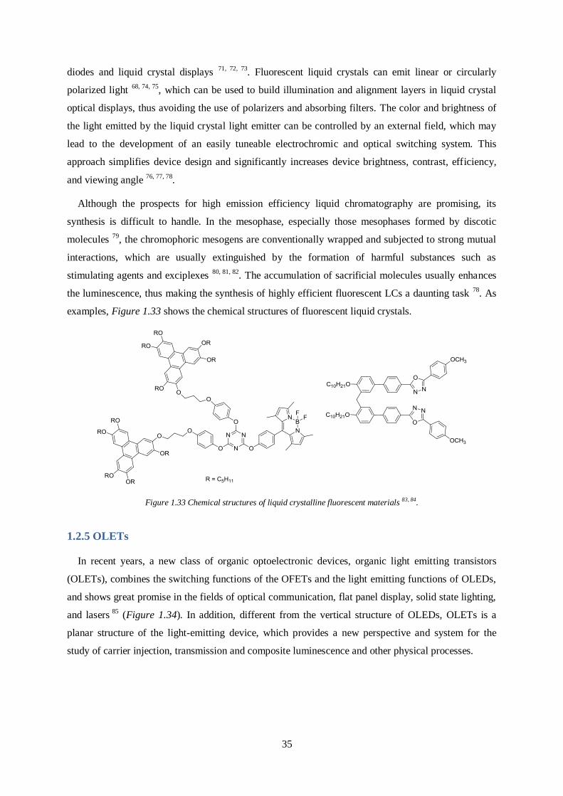
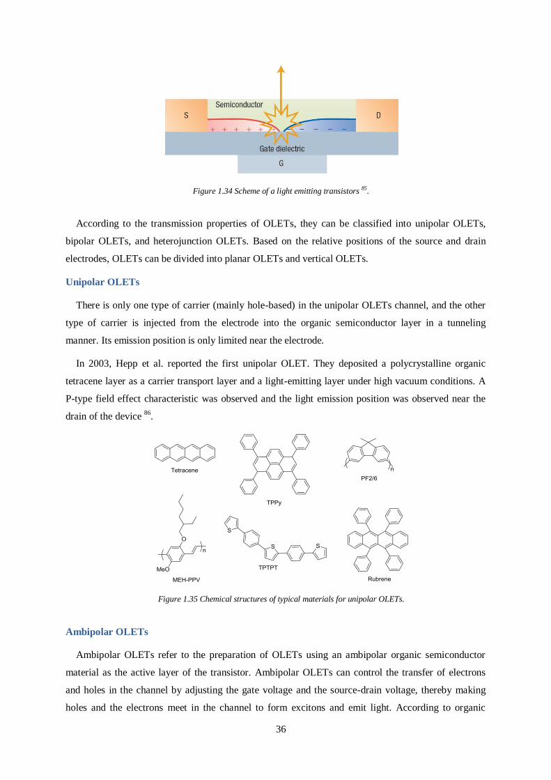


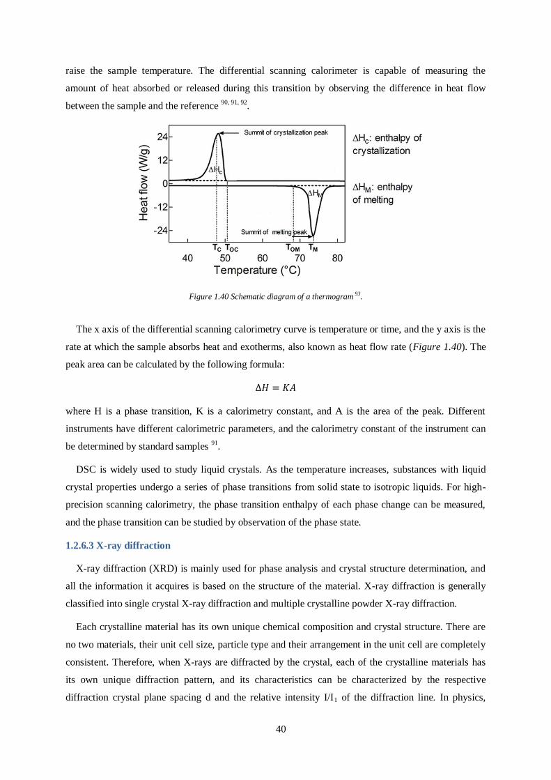


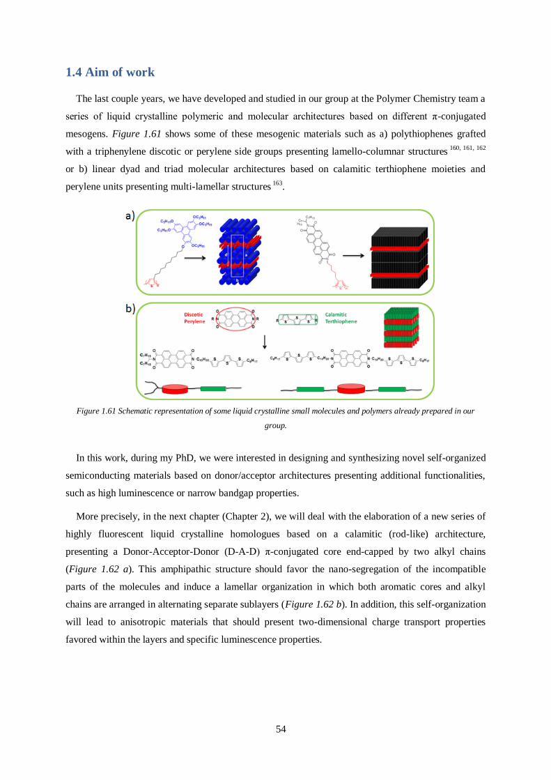


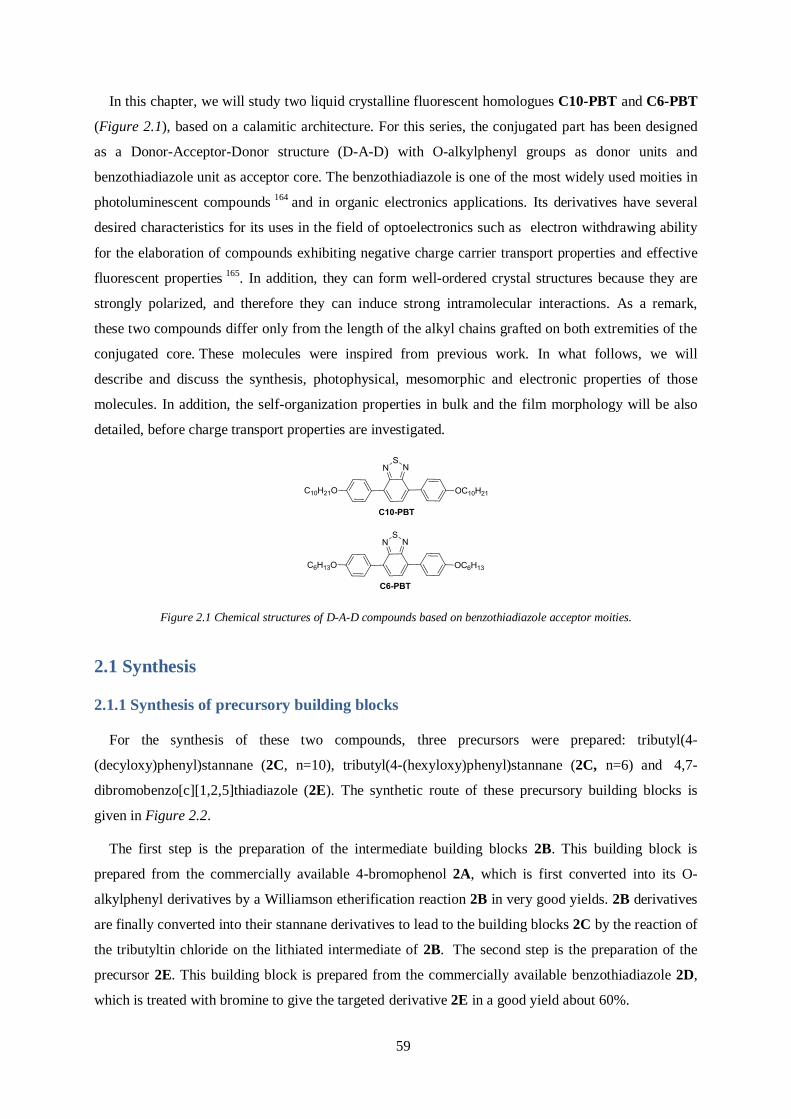
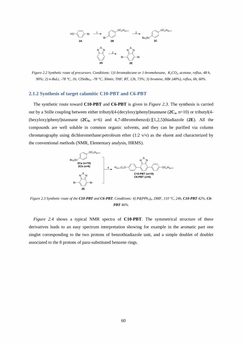


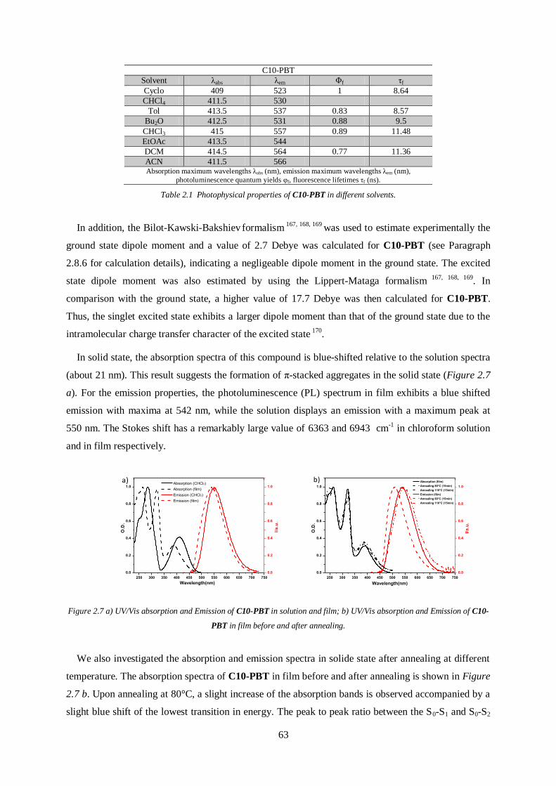


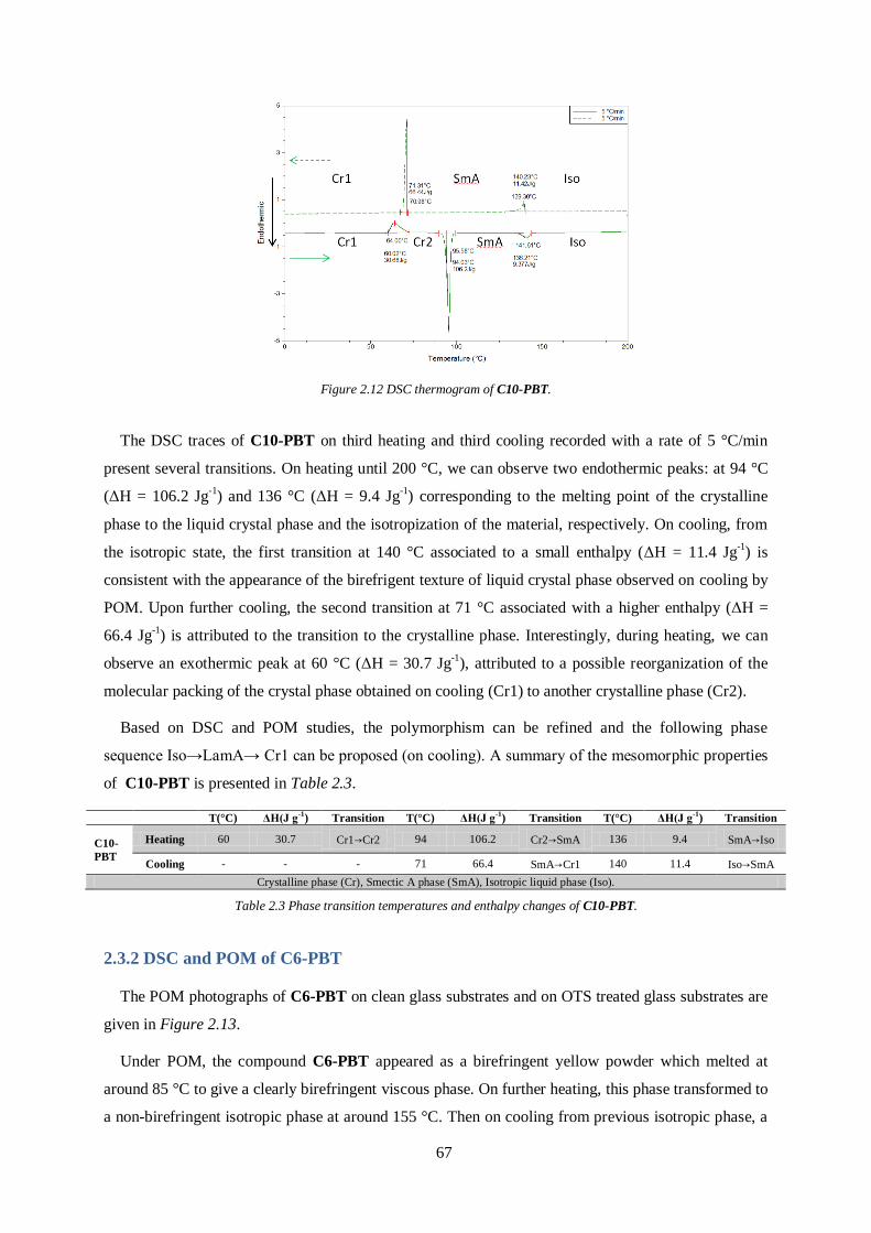


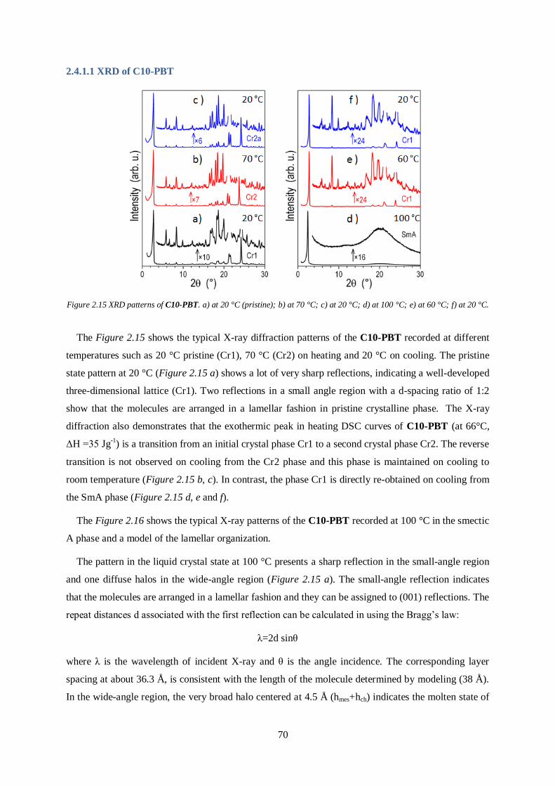


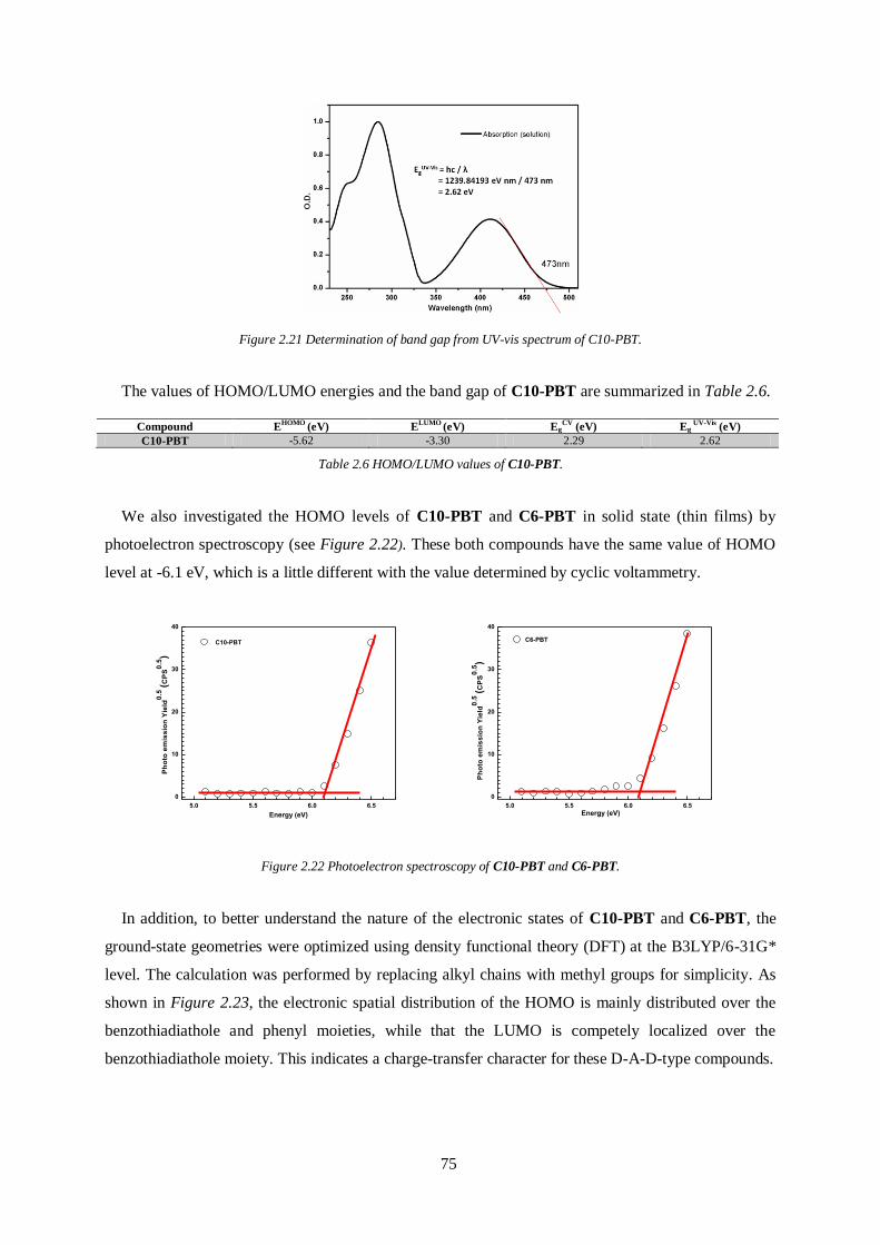


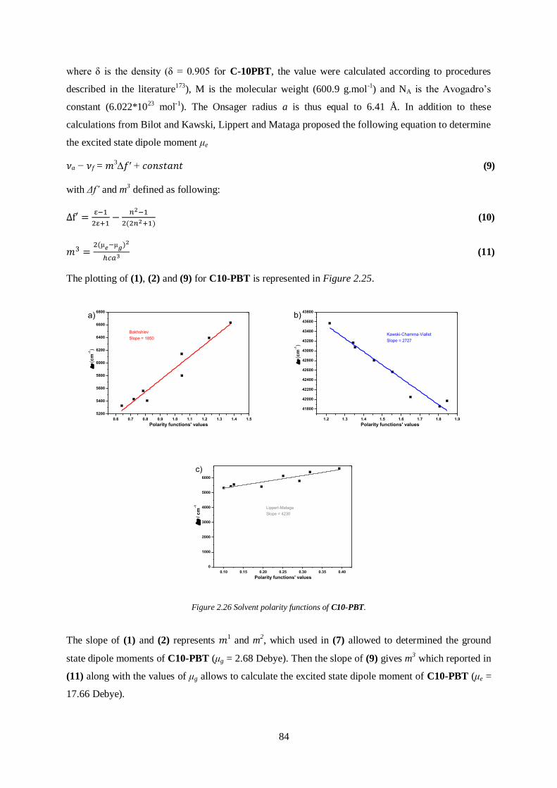

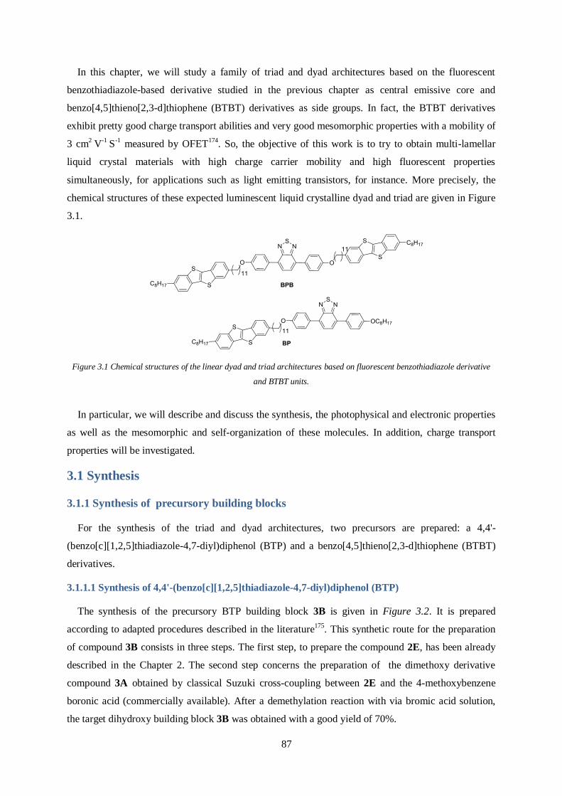


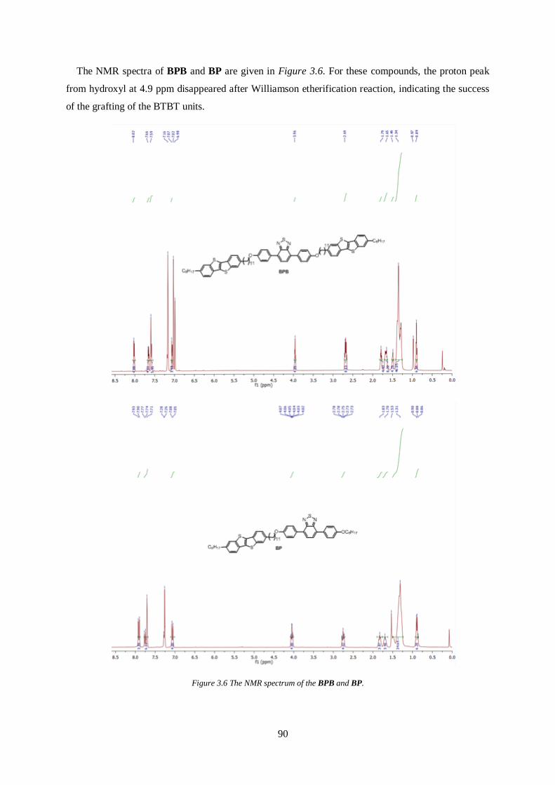

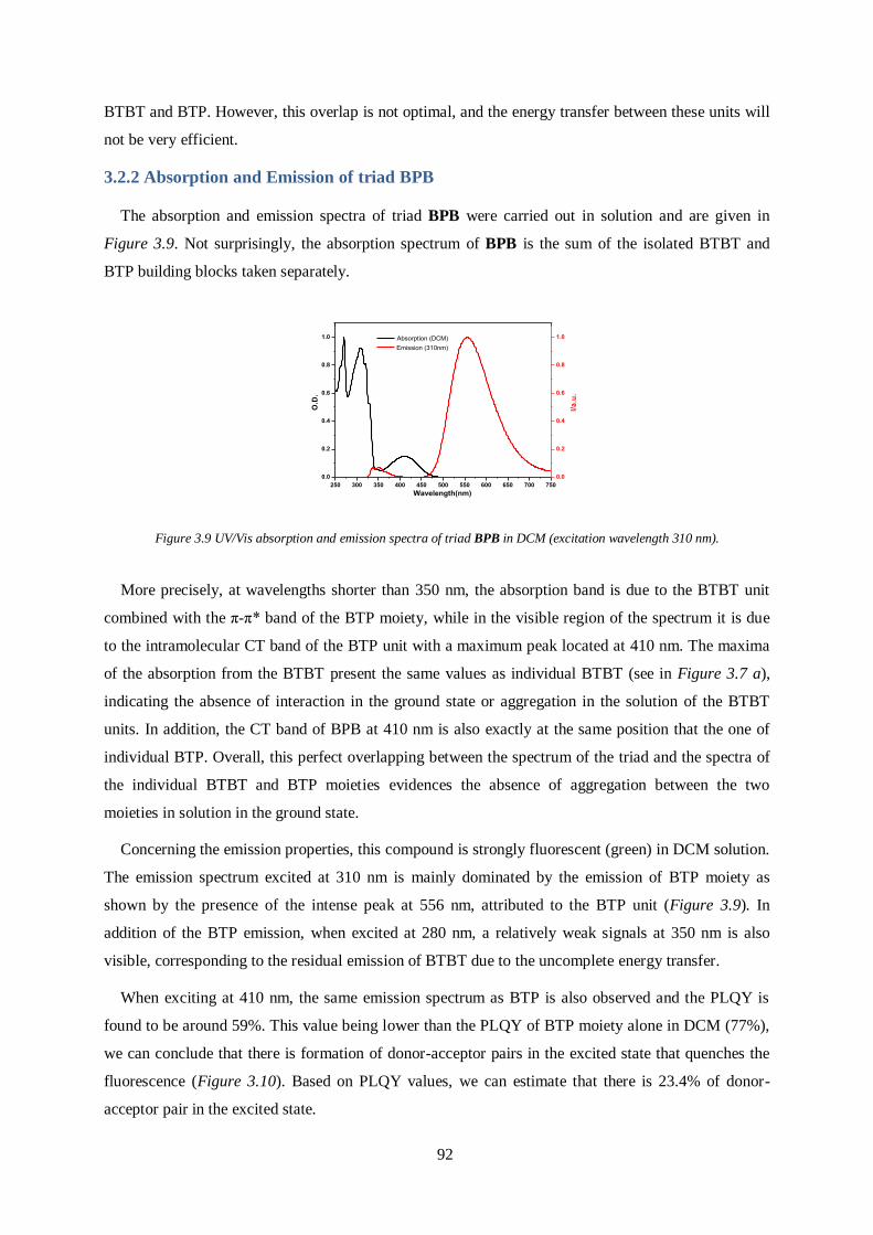
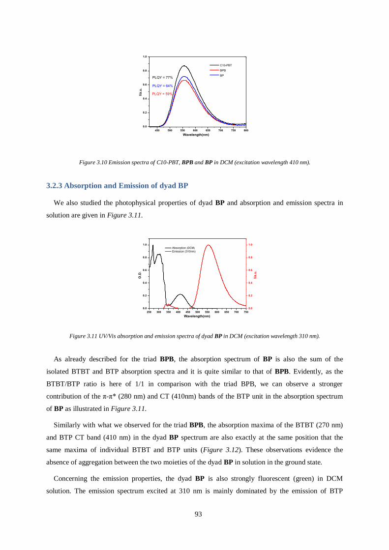

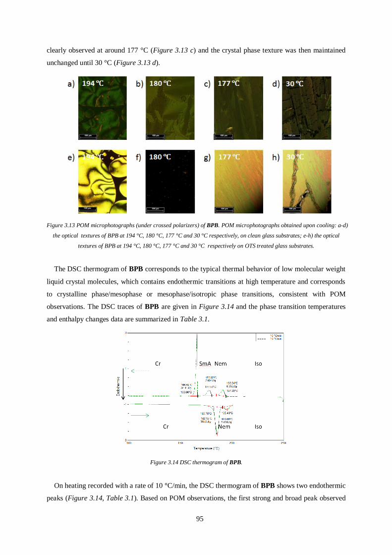


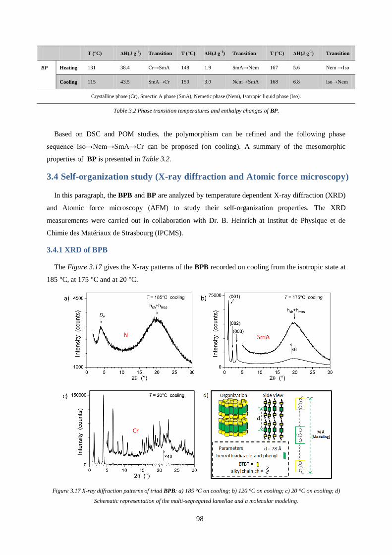


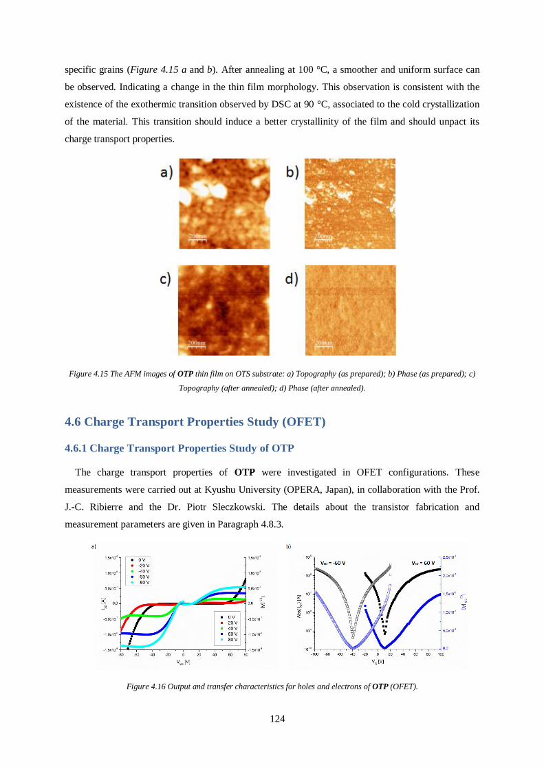


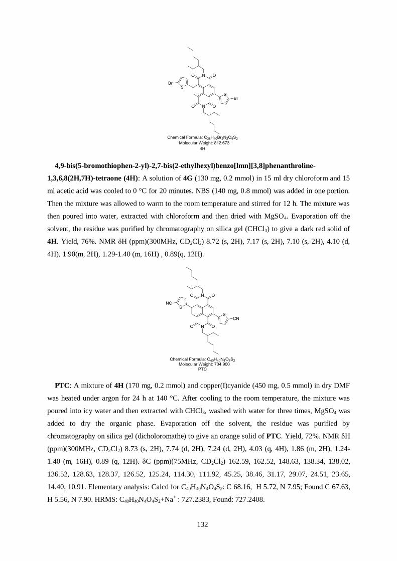


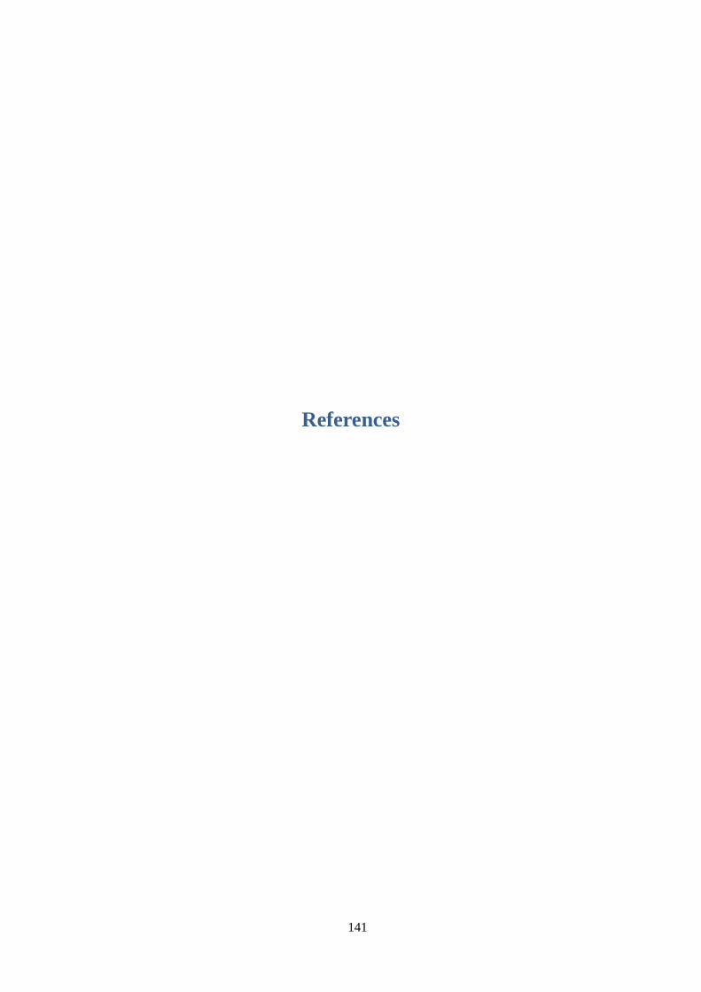


![Hydrogen-bonded donor–acceptor arrays at the solution ... · Hydrogen-Bonded Donor-Acceptor Arrays at the Solution-Graphite Interface Gangamallaiah Velpula,[a] Mengmeng Li,[b] ...](https://static.documents.pub/doc/80x56/60eb5095231c1d527c369a6c/hydrogen-bonded-donoraacceptor-arrays-at-the-solution-hydrogen-bonded-donor-acceptor.jpg)


