Contents lists available at SciVerse ScienceDirect
Sensors and Actuators B: Chemical
j o ur nal homep a ge: www.elsev ier .com/ locate /snb
ow voltage picoliter droplet manipulation utilizing electrowetting-on-dielectriclatforms
an-You Lin ∗, Erin R.F. Welch, Richard B. Fairepartment of Electrical and Computer Engineering, Duke University, Durham, NC 27708, USA
r t i c l e i n f o
rticle history:eceived 30 January 2012eceived in revised form 21 May 2012ccepted 5 July 2012vailable online 14 July 2012
eywords:icoliter droplet
a b s t r a c t
Picoliter droplets actuated on an electrowetting-on-dielectric (EWD) actuator are demonstrated. In thisstudy, the physical scaling of electrodes for 33 �m and 21 �m EWD devices resulted in droplets of 12 pland 5 pl being dispensed respectively in conjunction with 3 �m SU8 gaskets. The stacked multi-layerinsulators in the actuators consisted of 200 nm tantalum pentoxide (Ta2O5) and 200 nm parylene C filmsdeposited and coated with 70 nm of CYTOP. The voltages for dispensing droplets on chips without anyexternal pressure sources are 17.1 Vrms and 22 Vrms for these two sets of devices. A 12 pl droplet can be splitinto two 6 pl daughter droplets at 18.7 Vrms with 33 �m electrode devices. Droplet manipulation is also
igital microfluidicslectrowetting on dielectriculti-layer insulator
demonstrated with paramagnetic beads and buffer solutions with proteins. In addition, electrodes withinterlocking protrusions and special featured reservoir gasket are designed to facilitate droplet dispensingon these scaled EWD devices. In order to improve sealing of the two-piece sandwich EWD structure, asoft material, Norland Optical Adhesive (NOA), was coated on the top plate along with pressure on top.We demonstrate that based on fundamental theories and experiments, the dimensional scaling of EWD
limit
devices has not yet met a
. Introduction
In recent years, digital microfluidic manipulation of droplets haseen widely investigated as a platform for the transport of chem-
cal or biomedical liquids on biochips [1]. The ultimate goals areo reduce the laboratory reactants and procedures and miniatur-ze the instruments. With high throughput and minimized reagentonsumption, droplet-based systems can provide benefits to thepplications of medical diagnosis, drug delivery, point of care, envi-onmental monitoring, and basic scientific research with speed,onvenience, low-cost, and reliability.
An EWD device is a liquid droplet actuator based on control-ing charges at the interface of a liquid and an insulator over buriedlectrodes [1–3]. The droplets of microliter or nanoliter sizes cane promptly driven to a precise position, which is not achiev-ble by any other microfluidic methods [4]. EWD actuators haveeen shown to transport, split, mix, and dispense droplets fromn-chip reservoirs. Such liquid control gives more flexibility andetter choices for multiple applications performed on a commonlatform [5–10]. This technique has been adapted to applica-
ions, such as polymerase chain reaction (PCR) [11,12], clinicaliagnostics [13], proteomic sample preparation [14], DNA ligation15], simple separations [16], DNA sequencing [17,18] and other
complex biochemical [19,20] or biophysical [21] techniques. Formost biomedical or biochemical research, reagents and chemicalsamples are among the most expensive items used in experi-ments, as compared to machines and upstream costs. Miniaturizeddevices with picoliter droplets promise to provide the benefits ofhigh throughput, fast diagnosis, but with lower volumes of reagentrequired.
The electrode sizes used in previous studies were in the rangeof 750–1500 �m, and the droplet volumes were nano-to-microliterscale [3,6,7,9,22]. We previously reported a multi-layer insulatorEWD device, consisting of tantalum pentoxide (Ta2O5) and pary-lene C, and the smallest volume of 30 pl droplets could be dispensedwith 35 �m electrodes at 30 V [10]. Nelson and Kim [23] also fabri-cated monolithic EWD chips to actuate 100 pl droplets at 30 Vrms.Here, we experimentally demonstrate further scaled, low voltage,picoliter EWD devices. To allow for low-voltage operation, multi-layer insulators were still implemented. In addition, the interleavedelectrode design and the special gasket neck opening design facil-itate droplet dispensing on these scaled EWD actuators. A softmaterial layer of Norland Optical Adhesive (NOA) is coated onthe top plate to perform better sealing. The physical scaling ofelectrodes is designed and demonstrated for 33 �m and 21 �melectrodes to dispense droplets of 12 pl and 5 pl respectively with
3 �m gaskets at 17.1 Vrms and 22 Vrms on chip without any externalpressure sources. A 12 pl droplet can be dispensed and split intotwo 6 pl daughter droplets on 33 �m electrodes at the voltage aslow as 18.7 Vrms. Not only deionized (DI) water is demonstrated,
In addition, a small reservoir electrode was put in the frontof each reservoir to keep liquid close to the neck opening whileturned on, as shown in Fig. 4. The neck electrode was slightly largerthan the channel electrodes with three fingers on the opening side,
Y.-Y. Lin et al. / Sensors and
ut also droplets of buffer solution containing paramagnetic beadsnd with some concentration of proteins have been manipulatedn scaled devices.
. Electrowetting theory
Electrowetting is a principle extended from electrocapillar-ty, where an electric field changes the effective surface energyetween a solid electrode and a liquid interface to induce a drivingorce [3,24]. The mathematical model of electrowetting on dielec-ric that relates the applied voltage, V, and the droplet contact anglehange is given by the Lippmann–Young equation [25]:
os � = cos �0 + 1�SL
· εrε0
2tV2 (1)
here � and �0 are the contact angles with and without apply-ng voltage, �SL is the interfacial tension between the droplet andller medium, εr is the relative dielectric constant of the insula-or layer, ε0 is the permittivity of vacuum, and t is the thickness ofhe insulator. The droplet wets the electrode surface as the contactngle decreases and the surface becomes effectively less hydropho-ic along the contact line while voltage is increased. The variationf contact angle or wettability shift is caused predominantly by theharge-induced change in the solid–liquid interfacial tension [3].
Since the voltage applied changes the contact angle of theroplet and the interfacial tension between the electrode androplet, an actuator using EWD is proposed using this characteristico manipulate droplets in micro-channels [3,5,6], as shown in Fig. 1.
hen a voltage is applied on an adjacent electrode, the solid–liquidnterfacial tension (�SL) difference between active and non-activelectrodes induces a wetting force (fE) to distort the droplet andven to move the droplet forward if the force exceeds the dragorces and contact-line friction. Electrowetting actuators require aroplet to overlap the adjacent electrode when the droplet rests onhe biased electrode, so that the droplet can response to the voltagepplied on the adjacent electrode. Therefore, the interleaves elec-rodes were designed to facilitate the droplet actuation. Even if theroplet is slightly smaller than the electrode, the droplet can stillverlap the protrusions of adjacent electrodes and be wetted when
voltage is applied.According to our previous research results [2,10], the determin-
ng factors for low voltage EWD are the thickness and dielectriconstant of the insulator, and the fluid choices of droplets andller medium. Regardless of the insulator effects, the threshold
oltage ratio for actuation in air to actuation in oil is 1.9–2.5 [2].hus, all the EWD devices in this study were operated in a 1.5 cStilicone oil medium (�SL = 47 mN/m) to have lower actuation volt-ges and also prevent liquid vaporization. The other factor affecting
ig. 1. The side view of a EWD actuator with an applied voltage on the adjacentlectrode. The difference of �SL between two ends of the droplet induces the elec-rowetting force fE .
tors B 173 (2012) 338– 345 339
the actuation voltage is the thickness-to-dielectric-constant ratioof the insulator layer. We demonstrated that multi-layer insulatorEWD devices, consisting of stacked insulators of tantalum pentox-ide (Ta2O5, εr ∼ 23) and parylene C (εr ∼ 3) thin films, could provideadequate EWD operating voltage ranges that avoid insulator break-down and allow for reliable operation [10]. The stacked of insulatorsin this study were 200 nm Ta2O5 and 200 nm parylene C.
3. Device design and fabrication
3.1. Device design
The electrode sizes and configurations are very importantparameters in the physical dimensional scaling of EWD devices,because the electrowetting force is directly proportional to thearea and contact line of the droplet that overlaps the adjacentelectrode. Another key element is the gasket height and channelstructure design in the actuator, because the gasket thickness deter-mines the liquid volume per area driven by the electrowetting forceand affects the capability of liquid manipulation. The compatibledesign of electrodes and gaskets provides the best platform fordroplet manipulations on chip. The smallest electrode sizes everreported for electrowetting based devices were 100 �m and 35 �mwith 20 �m SU8 gaskets for 300 pl and 30 pl droplets manipulationrespectively [10].
Two different sizes of electrodes were designed to demonstratescaling. Dimensional-scaled electrodes were designed having sizes(L) of 33 �m with an 18 �m base and 6 �m round interlockingshapes, and L = 21 �m with a 10 �m base and 3 �m interlocking pro-trusions. Spaces between electrodes of 3 �m were used due to thephoto mask limitation of 3 �m features, as shown in Figs. 2 and 3.In order to provide more force and improve the droplet dispens-ing from the reservoirs, the reservoir electrode was designed witha trapezoidal shape with wide margins toward the neck, whichprovided larger wetting area, so that when this reservoir electrodewas turned on, the liquid would flow forward. Interlocking fingersfacilitated the droplet electrowetting, since the droplet would over-lap the adjacent electrodes while resting on one biased electrode[26]. The larger overlapping area allows for a significantly largerelectrowetting force when an adjacent electrode is activated.
Fig. 2. 33 �m electrode design with rounded interlocking fingers of 18 �m long,6 �m wide, and 3 �m spaces between electrodes.
340 Y.-Y. Lin et al. / Sensors and Actua
Fo
aeifatltr
3
stobbtwis
Fntf
ig. 3. 21 �m electrode design is similar to the 33 �m electrode device, with fingersf 10 �m long and 3 �m wide, and the spaces between electrodes are 3 �m.
llowing for a larger overlapping area, which resulted in a greaterlectrowetting force. Based on the previous experience of dispens-ng droplets on EWD devices, the reservoir neck opening helped toocus the extracted liquid finger and to assist pinch off of the liquidt the neck during liquid dispensing from a reservoir. However, ahick reservoir neck opening increased the difficulty of pulling outiquid. Thus, the gasket design at the reservoir neck opening wasapered to a point on either side to facilitate pulling liquid out ofeservoirs and pinching off liquid, as shown in Fig. 4.
.2. Device fabrication
Two-level metal EWD devices were fabricated on 2 cm × 3 cmilicon wafer pieces coated with 150 nm of SiO2 as a bulk insula-ion layer. With a two-level-metal process interconnects are routedn the lower level, which is insulated from the top level electrodesy a 1 �m silicon dioxide film. By burying the interconnecting wireseneath the electrodes, electrowetting is restricted to only the elec-
rode, and the footprint of the device can be made more compacthile allowing more flexibility in the electrode layout. The steps
n the two-level metal EWD device process are listed below, andhown in Fig. 5:
ig. 4. Special neck opening designs for 33 �m electrode devices. The body of theeck electrode is slightly larger than that of channel electrodes and three fingers athe opening side with the tapered gasket opening can facilitate pulling out liquidrom the reservoir.
tors B 173 (2012) 338– 345
1. The first layer of 70 nm Cr for the electrode connections wasdeposited by E-beam evaporation and patterned by Cr etchantwith approximately 3 �m positive photoresist S-1813.
2. 1 �m layer of PECVD SiO2 was deposited as an inter-layer insu-lator.
3. Via holes were next etched in a buffered oxide etchant (BOE,10 parts 40% NH4F and 1 part 49% HF) for 700 s, and filled withpatterned sputtered aluminum.
4. The second layer of 70 nm Cr for the electrodes and pads wasagain deposited and patterned (same as process 1).
5. 200 nm Ta2O5 were sputtered as the first layer dielectric layerof EWD by an RF dielectric sputtering system (Kurt Lesker PVD75) with a 99.99% Ta2O5 target. The deposition power was set at200 W and the deposition pressure was set at 15 mTorr with 10%oxygen percentages in the chamber.
6. An SU-8 gasket was spun on the wafer, and developed. The SU-8 gasket thickness (d) was dependant to the electrode size anddetermined by the desired d/L ratio of approximately 0.1–0.2[2,3,8]. For the devices with L = 33 �m and 21 �m, the gasketsthicknesses formed were 7 �m, 5 �m, and 3 �m.
7. A 200 nm second dielectric layer of parylene C was deposited inthe parylene coater.
8. Finally, the hydrophobic layer, composed of 70 nm CYTOP, wasspun on the wafers at 3000 rpm, then the film was annealed ona hot plate at 110 ◦C for 1 min, and the devices were placed in avacuum desiccator over night.
For one-level-metal devices, the process starts from step 4 ofthe two-level metal process, which avoids three photolithographysteps, and allows the whole fabrication to be finished in two to threework days. When the electrode number is fewer than the controlpads, which means each electrode can be independently controlledwithout complex bussing, this one-level-metal structure is a betterchoice to have devices tested in a shorter fabrication time.
The other fabricated part of a EWD device is the top plate, whichis a 3 cm × 5 cm acrylic (polycarbonate) piece that covers the entiredevice with additional space for the ground pad connection. Holes(approximately 500 �m in diameter) were drilled at the locations ofthe reservoir injection ports to dispense liquid into the reservoirs.For larger scale (100 �m and 35 �m electrodes) devices, the topplate was a piece of polycarbonate with sequential depositions ofITO and CYTOP serving as a ground layer and a hydrophobic layerrespectively [10]. Since the gasket height was lower than 10 �mand the structure of the device was smaller, the surface topographytolerance and the fabrication accuracy for SU8 decreased. The prob-lem first faced was that of sealing the channel, especially the edgesof the channel and the neck of the reservoir opening. The chan-nel and reservoir volumes became much smaller, so while loadingliquid onto the device, the pressure from the manually controlledpipette would squeeze the liquid out of the reservoir. Thus, the liq-uid would no longer be confined in the reservoir by the gasket. Dueto the pressure sealing method, a layer of elastic material on the topplate might be able to diminish the sealing issue caused by the sur-face roughness and fabrication inaccuracy. For an elastic and softmaterial, polydimethylsiloxane (PDMS) is the most common choicefor microfluidic applications, but PDMS would absorb silicone oil,which was the filler medium for EWD devices in this study. Instead,Norland Optical Adhesive (NOA, ThorLabs) was spin-coated on thetop plate with 2500 rpm for 60 s to get an approximately 50 �mthick film. The conductive polymer polydioctyl-bithiophene (PDOT,Aldrich) was then spin-coated for 150 nm as the ground layer fol-lowed by the hydrophobic layer of CYTOP. With pressure on the
top plate, the NOA layer could compensate the roughness of theSU8 surface at the edges and channel necks, and seal the chan-nel on the 7 �m and 5 �m gasket. However, for the gasket of 3 �mthickness, the end point of the channel neck could not be accurately
Y.-Y. Lin et al. / Sensors and Actuators B 173 (2012) 338– 345 341
proce
f2wld
4
itsdm
Fig. 5. The fabrication
abricated due to the limitation of photolithography, especially for1 �m electrodes. The neck edge was not sharply defined, so thathen liquid was pulled out of the reservoir into the channel, the
iquid flowed over the neck, which reduced the pinch-off duringispensing.
. Experimental results
Smaller volumes of liquid for EWD devices means scaling phys-cal dimensions, including electrode sizes and gasket heights. In
he present research, EWD devices were fabricated with electrodescaled to 33 �m and 21 �m. To verify the operation of the EWDevices, the droplet manipulations performed included transport,erging, splitting, and dispensing. Here, the operation of scaled
ss for EWD actuators.
devices was demonstrated with dispensing and splitting, whichwere the most difficult manipulations to be achieved on EWDdevices.
4.1. 33 �m electrodes
The electrodes were patterned as shown in Fig. 2. According toprevious reports [7,8], the best channel-height-to-electrode-sizeratio was 1:5 to provide the most efficient droplet manipulations,so that 5 �m and 3 �m SU8 gaskets were patterned for testing. The
oil-based medium of 1.5 ctS silicone oil with 0.02% TritonTM X-15was first introduced on the entire chip, and 10 nl DI water was thendispensed into the reservoirs by a pipette with the large reservoirelectrode turned on.
342 Y.-Y. Lin et al. / Sensors and Actua
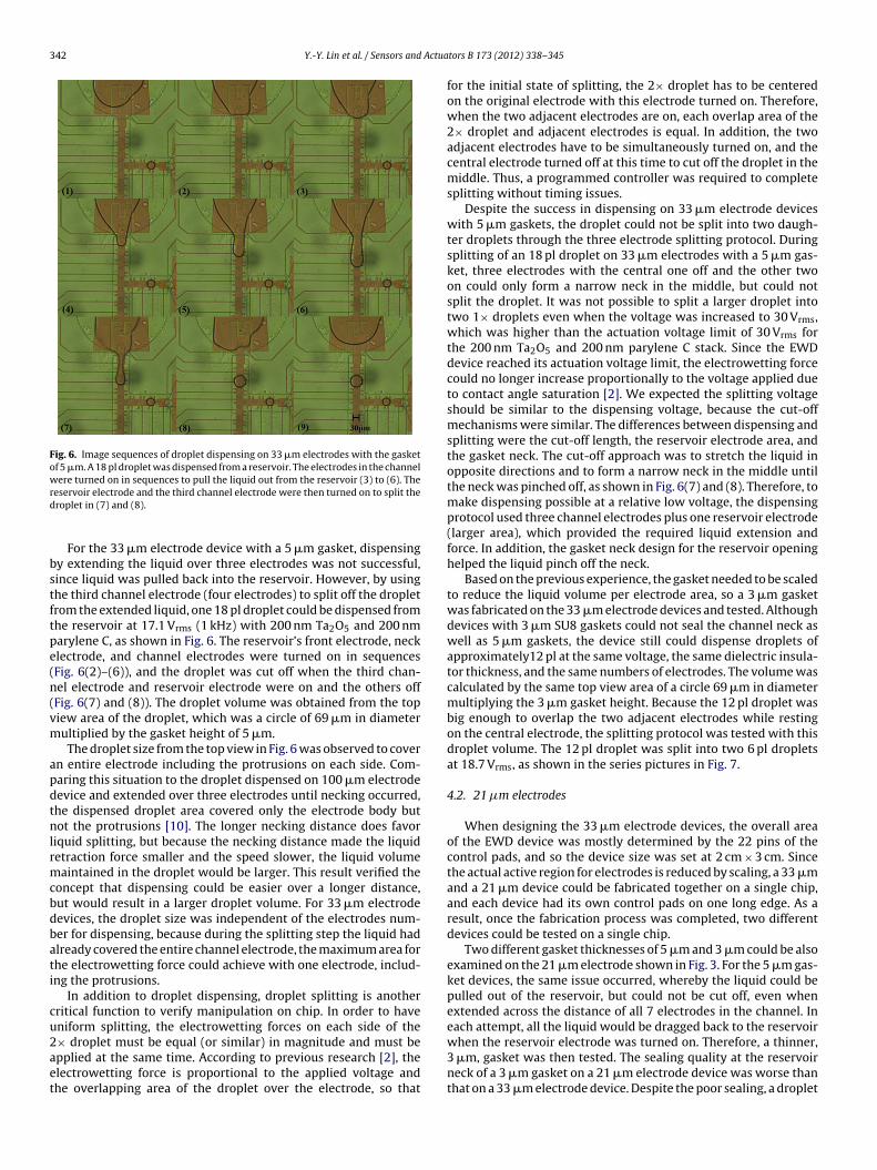
Fig. 6. Image sequences of droplet dispensing on 33 �m electrodes with the gasketof 5 �m. A 18 pl droplet was dispensed from a reservoir. The electrodes in the channelwere turned on in sequences to pull the liquid out from the reservoir (3) to (6). Therd
bstftpe(n(vm
apdtnlrmcbdbati
cu2aet
when the reservoir electrode was turned on. Therefore, a thinner,
eservoir electrode and the third channel electrode were then turned on to split theroplet in (7) and (8).
For the 33 �m electrode device with a 5 �m gasket, dispensingy extending the liquid over three electrodes was not successful,ince liquid was pulled back into the reservoir. However, by usinghe third channel electrode (four electrodes) to split off the dropletrom the extended liquid, one 18 pl droplet could be dispensed fromhe reservoir at 17.1 Vrms (1 kHz) with 200 nm Ta2O5 and 200 nmarylene C, as shown in Fig. 6. The reservoir’s front electrode, necklectrode, and channel electrodes were turned on in sequencesFig. 6(2)–(6)), and the droplet was cut off when the third chan-el electrode and reservoir electrode were on and the others offFig. 6(7) and (8)). The droplet volume was obtained from the topiew area of the droplet, which was a circle of 69 �m in diameterultiplied by the gasket height of 5 �m.The droplet size from the top view in Fig. 6 was observed to cover
n entire electrode including the protrusions on each side. Com-aring this situation to the droplet dispensed on 100 �m electrodeevice and extended over three electrodes until necking occurred,he dispensed droplet area covered only the electrode body butot the protrusions [10]. The longer necking distance does favor
iquid splitting, but because the necking distance made the liquidetraction force smaller and the speed slower, the liquid volumeaintained in the droplet would be larger. This result verified the
oncept that dispensing could be easier over a longer distance,ut would result in a larger droplet volume. For 33 �m electrodeevices, the droplet size was independent of the electrodes num-er for dispensing, because during the splitting step the liquid hadlready covered the entire channel electrode, the maximum area forhe electrowetting force could achieve with one electrode, includ-ng the protrusions.
In addition to droplet dispensing, droplet splitting is anotherritical function to verify manipulation on chip. In order to haveniform splitting, the electrowetting forces on each side of the× droplet must be equal (or similar) in magnitude and must be
pplied at the same time. According to previous research [2], thelectrowetting force is proportional to the applied voltage andhe overlapping area of the droplet over the electrode, so that
tors B 173 (2012) 338– 345
for the initial state of splitting, the 2× droplet has to be centeredon the original electrode with this electrode turned on. Therefore,when the two adjacent electrodes are on, each overlap area of the2× droplet and adjacent electrodes is equal. In addition, the twoadjacent electrodes have to be simultaneously turned on, and thecentral electrode turned off at this time to cut off the droplet in themiddle. Thus, a programmed controller was required to completesplitting without timing issues.
Despite the success in dispensing on 33 �m electrode deviceswith 5 �m gaskets, the droplet could not be split into two daugh-ter droplets through the three electrode splitting protocol. Duringsplitting of an 18 pl droplet on 33 �m electrodes with a 5 �m gas-ket, three electrodes with the central one off and the other twoon could only form a narrow neck in the middle, but could notsplit the droplet. It was not possible to split a larger droplet intotwo 1× droplets even when the voltage was increased to 30 Vrms,which was higher than the actuation voltage limit of 30 Vrms forthe 200 nm Ta2O5 and 200 nm parylene C stack. Since the EWDdevice reached its actuation voltage limit, the electrowetting forcecould no longer increase proportionally to the voltage applied dueto contact angle saturation [2]. We expected the splitting voltageshould be similar to the dispensing voltage, because the cut-offmechanisms were similar. The differences between dispensing andsplitting were the cut-off length, the reservoir electrode area, andthe gasket neck. The cut-off approach was to stretch the liquid inopposite directions and to form a narrow neck in the middle untilthe neck was pinched off, as shown in Fig. 6(7) and (8). Therefore, tomake dispensing possible at a relative low voltage, the dispensingprotocol used three channel electrodes plus one reservoir electrode(larger area), which provided the required liquid extension andforce. In addition, the gasket neck design for the reservoir openinghelped the liquid pinch off the neck.
Based on the previous experience, the gasket needed to be scaledto reduce the liquid volume per electrode area, so a 3 �m gasketwas fabricated on the 33 �m electrode devices and tested. Althoughdevices with 3 �m SU8 gaskets could not seal the channel neck aswell as 5 �m gaskets, the device still could dispense droplets ofapproximately12 pl at the same voltage, the same dielectric insula-tor thickness, and the same numbers of electrodes. The volume wascalculated by the same top view area of a circle 69 �m in diametermultiplying the 3 �m gasket height. Because the 12 pl droplet wasbig enough to overlap the two adjacent electrodes while restingon the central electrode, the splitting protocol was tested with thisdroplet volume. The 12 pl droplet was split into two 6 pl dropletsat 18.7 Vrms, as shown in the series pictures in Fig. 7.
4.2. 21 �m electrodes
When designing the 33 �m electrode devices, the overall areaof the EWD device was mostly determined by the 22 pins of thecontrol pads, and so the device size was set at 2 cm × 3 cm. Sincethe actual active region for electrodes is reduced by scaling, a 33 �mand a 21 �m device could be fabricated together on a single chip,and each device had its own control pads on one long edge. As aresult, once the fabrication process was completed, two differentdevices could be tested on a single chip.
Two different gasket thicknesses of 5 �m and 3 �m could be alsoexamined on the 21 �m electrode shown in Fig. 3. For the 5 �m gas-ket devices, the same issue occurred, whereby the liquid could bepulled out of the reservoir, but could not be cut off, even whenextended across the distance of all 7 electrodes in the channel. Ineach attempt, all the liquid would be dragged back to the reservoir
3 �m, gasket was then tested. The sealing quality at the reservoirneck of a 3 �m gasket on a 21 �m electrode device was worse thanthat on a 33 �m electrode device. Despite the poor sealing, a droplet
Y.-Y. Lin et al. / Sensors and Actua
Fig. 7. Image sequences of droplet splitting on 33 �m electrodes with the 3 �mheight gasket. One 12 pl droplet (2× droplet) were dispensed from a reservoir to thept
odtnF
Fcpr
osition in (1). Two adjacent electrodes were turned on with 18.7 Vrms to split intowo 6 pl droplets simultaneously.
f approximately 5 pl was still able to be dispensed at 22 Vrms as
emonstrated in Fig. 8 (Video 1). However, due to the sealing issue,he liquid being pulled out of the reservoir overflowed the reservoireck and the required narrow neck was not formed, as shown inig. 8(3)–(5). As a result, four electrodes were not enough to split
ig. 8. Image sequences of droplet dispensing on 21 �m electrodes with the gasket of 3 �hannel were turned on in sequences to pull the liquid out from the reservoir, from (2) tooor sealing, the liquid being pulled out of the reservoir overflowed the gasket neck and
equired to dispense.
tors B 173 (2012) 338– 345 343
the droplet from the reservoir, so that the fifth electrode (Fig. 8(6))and a higher voltage (compared to the same thickness of dielectriclayers on other scale devices) were required to hold the dropleton the electrode from the retraction force of liquid as the reser-voir electrode was on. Although dispensing was reproducible on21 �m electrode devices with 3 �m gaskets, splitting could not beaccomplished. The 2× droplet could not be cut off at 30 Vrms, whichwas above the actuation voltage limit. This issue was also observedin previous devices, so further scaling of the gaskets was needed.Therefore, a 1 �m SU8 gasket was fabricated and tested on a 21 �melectrode device, but this gasket was too thin to maintain liquidin the reservoir area with pressure sealing, even on a NOA coatedtop plate. While dispensing liquid from a pipette into an on-chipreservoir, liquid would overflow and spread over the entire device.
During the experiments of fabricating and testing the picol-iter scale devices, all the manipulations of scaling devices wereoperated on chip without any external forces, relying only on elec-trowetting forces. Although many different parameters, such astypes of surfactants, liquid volumes, and gasket thicknesses anddesigns needed to be considered in real situations while dispensingand splitting, the results of these studies verified and demonstratedthe basic theories and concepts of scaling EWD devices.
4.3. EWD actuator implementation
DNA pyrosequencing has been demonstrated in both nanoliterand 300 pl EWD devices [17,18]. For a simplified verification, DNApyrosequencing on EWD devices included manipulation of param-
agnetic beads and buffer solutions with luciferase and ATP withluciferin. Here, these solutions were also demonstrated on thescaled devices of 33 �m and 21 �m electrodes. Invitrogen Dyn-abeads M-270 2.8 �m streptavidin-functionalized paramagnetic
m. A 5 pl droplet was dispensed from a reservoir at 22 Vrms. The electrodes in the (5). The reservoir electrode was turned on to split the droplet in (6). Because of theno narrow neck was formed (3)–(5), and five electrodes and a higher voltage were
344 Y.-Y. Lin et al. / Sensors and Actuators B 173 (2012) 338– 345
F ir on ai quenca and (
bbgdacl3
(nriaic1tob
rwc(tba
TT
ig. 9. 2.8 �m paramagnetic beads in a 12 pl droplet were dispensed from a reservonto the reservoir with a pipette. The electrodes in the channel were turned on in send the third channel electrode were then turned on to split the bead droplet in (7)
ead solution was dispensed into the reservoir, and droplets coulde dispensed on chip into the channel for both devices with 3 �maskets. A 12 pl bead droplet was dispensed on a 33 �m electrodeevice, as shown in Fig. 9. The dispensing voltages were the sames needed for DI water manipulation mentioned above. Reservoirsontaining buffer solutions of 1 �g/�l luciferase and 400 �g/mluciferin with 0.1 �M ATP [18] were dispensed as droplets on both3 �m and 21 �m electrode EWD devices.
In the pyrosequencing reaction, the amount of pyrophosphatePPi) produced by the incorporation reaction between DNA anducleotides is a linear response to the amount of nucleotideseacted. ATP, which is produced by an enzymatic reaction with PPi,s used in the chemiluminescent reaction that produces light thatllows the amount of nucleotides reacted to be determined dur-ng the sequencing of unknown DNA. Using an externally mountedooled CCD camera (CoolSnap ES2, Photometrics) mounted with a0× objective (Epiplan-Neofluar), we were able to create a calibra-ion curve relating light intensity versus reactant ATP concentrationn 300 pl chips [18]. For 100 pl chips, the light intensity decreasedy about 1/3.
As the device dimensions are further scaled, the ATP–luciferineaction was implemented on 33 �m and 21 �m electrode devicesith 3 �m and 5 �m gaskets. Both substrate and enzyme solutions
ould be successfully dispensed and merged on all these devices
Video 2) with the same concentrations used for 100 pl droplet reac-ions, but the resulting light intensity was too low to be detectedy the external cooled CCD camera even with long exposure timesnd 8 × 8 pixel binning. As an alternative to the cooled CCD camera,
able 1he results of scaled EWD devices. The cross line means splitting failures.
a The dielectric layer are 135 nm Ta2O5 and 180 nm parylene C.
33 �m electrode device with a 3 �m gasket. The bead solution was first dispensedes to pull the bead solution out from the reservoir (3) to (6). The reservoir electrode8).
an EMCCD camera (QuantEM, Photometrics), whose working tem-perature is −30 ◦C and quantum efficiency at 560 nm wavelength is92%, was also tested as a sensor of the chemiluminescent signal, butno light could be detected with such small droplet volumes. Theseresults suggest that better coupling of light out of the droplet itselfis required using integrated sensors built into the top plate of theactuator, as demonstrated by Luan et al. [19]. However, the EWDactuator was demonstrated and verified as a platform to manip-ulate picoliter droplets on demand, and could be implemented todifferent applications in the future.
5. Conclusions
The work reported in this study has demonstrated dimensionalscaling of EWD actuators into the picoliter volume range. Pico-liter actuator fabrication has required new multi-layer insulatorstructures, interleaved electrode design to increase electrowettingforces, and improved gasket designs to allow for the sealing ofthe two plate sandwich actuator as well as adequate flow focus-ing for dispensing droplets from on-chip reservoirs. With dielectriclayers of 200 nm Ta2O5 and parylene C, the results of different elec-trode sizes and gasket thicknesses are listed in Table 1. The dropletsize of 5 pl is the smallest volume reported in view of all the EWDmicrofluidic research results published up to date. In addition, para-
magnetic beads and buffer solutions with luciferase and luciferinwith ATP were manipulated on these scaled devices. These resultshave demonstrated that the scaled EWD actuators can be imple-mented in real biomedical or biochemical applications.
l) Dispensing voltage (Vrms) Splitting voltage (Vrms)
11.4a –17.7 17.717.1 –17.1 18.722 –
Actua
fciIniweto
A
t
A
t
R
[
[
[
[
[
[
[
[
[
[
[
[
[
[
[
[
[
trochemical Society, past Editor-in-Chief of the Proceedings of the IEEE, and he has
Y.-Y. Lin et al. / Sensors and
These results also show that two plate EWD devices are feasibleor gasket thicknesses smaller than 10 �m. However, the physi-al scaling of EWD devices appears to face a significant difficultyn confining liquid in a reservoir with a gasket thinner than 3 �m.n addition, dispensing liquid from a macro-scale pipette onto theano-scale on-chip reservoir becomes a challenge due to the lim-
ted capillary filling for 3 �m gaskets. Despite this sealing problem,e believe the electrowetting theory is still viable for smaller scale
lectrodes, but due to the electrode-size-to-channel-height ratio,he submicron dimension channel fabrication would be the keybstacle to overcome.
cknowledgement
This research was supported by grant # R01HG004354-01 fromhe National Institutes of Health.
ppendix A. Supplementary data
Supplementary data associated with this article can be found, inhe online version, at http://dx.doi.org/10.1016/j.snb.2012.07.022.
eferences
[1] R.B. Fair, Digital microfluidics: is a true lab-on-a-chip possible? Microfluidicsand Nanofluidics 3 (3) (2007) 245–281.
[3] M.G. Pollack, R.B. Fair, A.D. Shenderov, Electrowetting-based actuation of liquiddroplets for microfluidic applications, Applied Physics Letters 77 (11) (2000)1725–1727.
[4] P. Tabeling, Introduction to Microfluidics, Oxford University Press, New York,2005.
[5] S.K. Cho, S.-K. Fan, H. Moon, C.-J. Kim, Towards digital microfluidiccircuits: creating, transporting, cutting and merging liquid droplets byelectrowetting-based actuation, in: Proceedings IEEE Micro Electro MechanicalSystems, vol. 11, 2002, pp. 454–461.
[6] S.K. Cho, H. Moon, C.-J. Kim, Creating, transporting, cutting, and merging liq-uid droplets by electrowetting-based actuation for digital microfluidic circuits,Journal of Microelectronic Systems 12 (1) (2003) 70–80.
[7] M. G. Pollack, Electrowetting-based microactuation of droplets for digitalmicrofluidics, Ph.D. Thesis, Duke University, 2001.
[8] M.G. Pollack, A.D. Shenderov, R.B. Fair, Electrowetting-based actuation ofdroplets for integrated microfluidics, Lab on a Chip 2 (2002) 96–101.
[9] Y. Li, W. Parkes, L.I. Haworth, A.A. Stokes, K.R. Muir, P. Li, A.J. Collin, N.G.Hutcheon, R. Henderson, B. Rae, A.J. Walton, Anodic Ta2O5 for CMOS com-patible low voltage electrowetting-on-dielectric device fabrication, Solid StateElectronics 52 (2008) 1382–1387.
10] Y.-Y. Lin, R.D. Evans, E. Welch, B.-N. Hsu, A.C. Madison, R.B. Fair, Low volt-age electrowetting-on-dielectric platform using multi-layer insulators, Sensors
and Actuators B 150 (1) (2010) 465–470.
11] T. Zhang, K. Chakrabarty, R.B. Fair, Behavioral modeling and performanceevaluation of microelectrofluidics-based PCR systems using System C, IEEETransactions on Computer-Aided Design of Integrated Circuits and Systems23 (6) (2004) 843–858.
tors B 173 (2012) 338– 345 345
12] M.G. Pollack, P.Y. Paik, A.D. Shenderov, V.K. Pamula, F.S. Dietrich, R.B. Fai, Inves-tigation of electrowetting-based microfluidics for real-time PCR applications,Proceedings of Micro Total Analysis Systems (2003) 619–622.
13] V. Srinivasan, V.K. Pamula, R.B. Fair, An integrated digital microfluidic lab-on-a-chip for clinical diagnostics on human physiological fluids, Lab on a Chip 4(2004) 310–315.
14] H. Moon, A.R. Wheeler, R.L. Garrell, J.A. Loo, C.J. Kim, An integrated digitalmicrofluidic chip for multiplexed proteomic sample preparation and analysisby MALDI-MS, Lab on a Chip 6 (9) (2006) 1213–1219.
15] H.-C. Lin, Y.-J. Liu, D.-J. Yao, Core shell droplets for parallel DNA ligation of anultra-micro volume using an EWOD microfluidic system, Journal of LaboratoryAutomation 15 (3) (2010) 210–215.
16] S.K. Cho, Y. Zhao, C.J. Kim, Concentration and binary separation of micro parti-cles for droplet-based digital microfluidics, Lab on a Chip 7 (2007) 490–498.
17] D.J. Boles, J.L. Benton, G.J. Siew, M.H. Levy, P.K. Thwar, M.A. Sandahl, J.L. Rouse,L.C. Perkins, A.P. Sudarsan, V.K. Pamula, V. Srinivasan, R.B. Fair, P.B. Griffin, A.E.Eckhardt, M.G. Pollack, Droplet-based pyrosequencing using digital microflu-idics, Analytical Chemistry 83 (22) (2011) 8439–8447.
18] E.R.F. Welch, Y.-Y. Lin, A. Madison, R.B. Fair, Picoliter DNA sequencing chem-istry on an electrowetting-based digital microfluidic platform, BiotechnologyJournal 6 (2011) 165–176.
19] L. Luan, R. Evans, N.M. Jokerst, R.B. Fair, Integrated optical sensor in a digitalmicrofluidic platform, IEEE Sensors Journal 8 (2008) 628–635.
21] Y.-Y. Lin, C.-W. Lin, L.-J. Yang, A.-B. Wang, Micro-viscometer based on elec-trowetting on dielectric, Electrochimica Acta 52 (2007) 2876–2883.
22] H. Moon, S.K. Cho, R.L. Garrell, C.-J. Kim, Low voltage electrowetting-on-dielectric, Journal of Applied Physics 92 (7) (2002) 4080–4087.
23] W.C. Nelson, C.J. Kim, Monolithic fabrication of EWOD chips for picoliterdroplets, Journal of Microelectronic Systems 20 (2011) 1419–1427.
24] M.G. Lippmann, Relations entre les phénomènes electriques et capillaires,Annales de chimie et de physique 5 (11) (1875) 494–549.
25] B. Berge, Electrocapillarite et mouillage de films isolants par l’eau, Comptesrendus de l’Académie des sciences 317 (2) (1993) 157–163.
26] J. Berthier, Microdrops and Digital Microfluidics, William Andrew, New York,2008.
Biographies
Yan-You Lin received his B.S. degree in electronics engineering from National ChiaoTung University, Taiwan in 2004; M.S. degree in electrical engineering from NationalTaiwan University, Taipei, Taiwan, in 2006; Ph.D. degree in electrical and com-puter engineering from Duke University, Durham, NC, in 2011. His research interestsinclude microfluidics, lap-on-a-chip technologies, and microsystems design.
Erin R.F. Welch received her PhD in analytical chemistry from the University ofNorth Carolina at Chapel Hill in 2009. She was a postdoctoral fellow in Electrical andComputer Engineering at Duke University, with interests in general microfluidics,digital electrowetting, DNA sequencing and analysis.
Richard B. Fair is a Lord-Chandran Professor of Engineering at Duke. His currentresearch areas include digital microfluidic devices, applications, and technology. Hehas published over 150 papers in refereed journals and conference proceedings,written 11 book chapters, edited nine books or conference proceedings, and givenover 130 invited talks. Dr. Fair is also a Fellow of the IEEE, a Fellow of the Elec-
served as associate editor of the IEEE Transactions on Electron Devices. He is a recip-ient of the IEEE Third Millennium Medal (2000) and the 2003 Solid State Science andTechnology Prize and Medal from the Electrochemical Society, which was presentedin Paris.