37
Series 2000 Reader System Mini-RFM RI-RFM-003C Reference Guide Literature Number: SCBU048 (11-06-21-069) June 2008
| Date post: | 12-Jun-2018 |
| Category: |
Documents |
| Upload: | nguyenhanh |
| View: | 215 times |
| Download: | 0 times |

Series 2000 Reader SystemMini-RFM RI-RFM-003C
Reference Guide
Literature Number: SCBU048 (11-06-21-069)June 2008

2 SCBU048 (11-06-21-069)–June 2008Submit Documentation Feedback

Contents
Preface ............................................................................................................................... 5
1 Introduction ............................................................................................................... 71.1 General........................................................................................................................ 81.2 System Overview ............................................................................................................ 81.3 Product Description.......................................................................................................... 81.4 Mechanical Construction.................................................................................................... 9
2 Electrical Description ................................................................................................ 112.1 General ...................................................................................................................... 122.2 Transmitter .................................................................................................................. 122.3 Receiver ..................................................................................................................... 142.4 Antenna Circuit ............................................................................................................. 14
3 Connectors .............................................................................................................. 173.1 Connector Location ........................................................................................................ 183.2 Connector ST1.............................................................................................................. 193.3 Connector ST2.............................................................................................................. 193.4 Antenna Connector ........................................................................................................ 20
4 Specifications .......................................................................................................... 214.1 Recommended Operating Conditions ................................................................................... 224.2 Electrical Characteristics .................................................................................................. 234.3 Timing Characteristics ..................................................................................................... 254.4 Mechanical Data............................................................................................................ 25
5 Installation and Use .................................................................................................. 275.1 Mechanical Mounting ...................................................................................................... 285.2 Supply Voltage.............................................................................................................. 285.3 Receiver Signal Strength Output RXSS- ................................................................................ 305.4 Programming a Transponder ............................................................................................. 315.5 Antenna Requirements .................................................................................................... 325.6 Antenna Tuning............................................................................................................. 33
5.6.1 To Switch On the Transmitter ................................................................................... 335.6.2 To Tune the Antenna Circuit..................................................................................... 335.6.3 To Detect the Correct Tuning.................................................................................... 345.6.4 Tuning Procedure ................................................................................................. 34
6 Warnings, Cautions, and Notices ................................................................................ 356.1 FCC/Telecommunications Regulations.................................................................................. 366.2 Important Note to Purchasers/Users of the Mini-RFM in the USA................................................... 366.3 Warning...................................................................................................................... 366.4 Cautions ..................................................................................................................... 36
SCBU048 (11-06-21-069)–June 2008 Contents 3Submit Documentation Feedback

www.ti.com
List of Figures1-1 The RI-RFM-003C ........................................................................................................... 92-1 Mini-RFM Block Diagram.................................................................................................. 132-2 Mini-RFM's Antenna Circuit ............................................................................................... 153-1 Top View .................................................................................................................... 184-1 Maximum Supply Current I_VSP versus t_off (Power Stage) ........................................................ 244-2 Mechanical Dimensions - Top View ..................................................................................... 264-3 Mechanical Dimensions - Side View..................................................................................... 265-1 PCB Mounting Proposal ................................................................................................... 285-2 Supply Line Wiring for Short Supply Lines.............................................................................. 295-3 Supply Line Wiring for a Separated Power Supply .................................................................... 295-4 Synchronization Output Control - Digital Adjustment .................................................................. 305-5 Synchronization Output Control - Analog Adjustment ................................................................. 315-6 Write Pulse Timing for TXCT- ............................................................................................ 315-7 Stick Antenna RI-ANT-P02A.............................................................................................. 33
List of Tables3-1 Module Connector - ST1 .................................................................................................. 193-2 Antenna Tuning Connector - ST2 ........................................................................................ 193-3 Antenna Connector ........................................................................................................ 20
4 List of Figures SCBU048 (11-06-21-069)–June 2008Submit Documentation Feedback

PrefaceSCBU048 (11-06-21-069)–June 2008
Read This First
Edition One - June 2008This is the First edition of this manual, it describes the following equipment:
Texas Instruments (TI™) Mini-Radio Frequency Module RI-RFM-003C
About This GuideThis manual describes the TI Mini-Radio Frequency Module (Mini-RFM). It provides the information thatyou will need in order to install the Mini-RFM into your RFID system. It is generally targeted at systemsintegrators or value-added resellers.
Regulatory, safety and warranty notices that must be followed are given in Chapter 6.
TI is a trademark of Texas Instruments.
SCBU048 (11-06-21-069)–June 2008 Read This First 5Submit Documentation Feedback

Conventions www.ti.com
Conventions
WARNINGA WARNING IS USED WHERE CARE MUST BE TAKEN, OR ACERTAIN PROCEDURE MUST BE FOLLOWED IN ORDER TOPREVENT INJURY OR HARM TO YOUR HEALTH.
CAUTIONThis indicates information on conditions that must be met, or a procedure whichmust be followed, that if not heeded could cause permanent damage to theequipment or software.
Note: Indicates conditions that must be met, or procedures which must be followed, to ensureproper functioning of the equipment or software.
Note: Indicates information that makes usage of the equipment or software easier.
If You Need AssistanceApplication Centers are located in Europe, North and South America, the Far East and Australia to providedirect support. For more information, please contact your nearest TI Sales and Application Center. Thecontact addresses can be found on our home page: http://www.ti-rfid.com
TrademarksThe TI logo and the words TI and Tag-it are trademarks or registered trademarks of Texas Instruments.
6 Read This First SCBU048 (11-06-21-069)–June 2008Submit Documentation Feedback

Chapter 1SCBU048 (11-06-21-069)–June 2008
Introduction
This chapter introduces you to the Mini-RFM. It tells you what the module is for, provides an overview ofthe complete system and the product itself. It also provides a mechanical description of the construction ofthe Mini-RFM.
Topic .................................................................................................. Page
1.1 General...................................................................................... 81.2 System Overview ........................................................................ 81.3 Product Description .................................................................... 81.4 Mechanical Construction ............................................................. 9
SCBU048 (11-06-21-069)–June 2008 Introduction 7Submit Documentation Feedback

1.1 General
1.2 System Overview
1.3 Product Description
General www.ti.com
This manual provides information about the TI™ Mini-Radio Frequency Module RI-RFM-003C. It describesthe module and how to integrate it into your RFID system.
This guide should be used in conjunction with the RFM Sequence Control Reference Manual (documentnumber 11-06-21-049) which describes the timing and sequence of radio communications between the TItransponder and the radio frequency module.
The three major parts of a TI system are the transponder, antenna and reader.
When a transponder is to be read, the reader sends out a 134.2 kHz power pulse lasting approximately50 ms to the antenna. The field generated by this power pulse is collected by the antenna in thetransponder that is tuned to the same frequency. This received energy is stored in a small capacitor withinthe transponder. When the power pulse has finished, the transponder immediately transmits its data backto the reader, using the energy stored within its capacitor as the power source.
The Mini-Radio Frequency Module is an integral part of a TI system, together with a control module or unitand an antenna it is used for wireless identification of TI transponders.
Main tasks of the RF module are to send an energizing signal via the antenna to initialize a TItransponder, to demodulate the received transponder identification signal and to write to a transponder.The RF module delivers a digital data stream and a clock signal for further processing to its control unit ormodule. Furthermore a field strength dependent digital output is available for synchronization purposes.
8 Introduction SCBU048 (11-06-21-069)–June 2008Submit Documentation Feedback

1.4 Mechanical Construction
www.ti.com Mechanical Construction
Figure 1-1. The RI-RFM-003C
Its small size and low supply voltage makes the Mini-RFM well suited for portable reading/writing units, aswell as for stationary equipment where medium read/write range and speed are sufficient.
The data input and output lines are compatible with the HCMOS-logic family.
The RF module has a simple mechanical construction where all the components are mounted on theprinted circuit board (PCB). The components of the upper and lower side of the PCB are protected bymetal shields. The PCB also carries the connectors ST1, ST2 and the antenna terminals A1 to A3, whichare captive nuts soldered to the PCB. These captive nuts allow durable low resistance connection with thering terminals of the antenna.
SCBU048 (11-06-21-069)–June 2008 Introduction 9Submit Documentation Feedback

Introduction10 SCBU048 (11-06-21-069)–June 2008Submit Documentation Feedback

Chapter 2SCBU048 (11-06-21-069)–June 2008
Electrical Description
This chapter provides an electrical description to block diagram level of how the Mini-RFM works.
Topic .................................................................................................. Page
2.1 General .................................................................................... 122.2 Transmitter............................................................................... 122.3 Receiver................................................................................... 142.4 Antenna Circuit......................................................................... 14
SCBU048 (11-06-21-069)–June 2008 Electrical Description 11Submit Documentation Feedback

2.1 General
2.2 Transmitter
General www.ti.com
The RF module is the interface between the TI transponder and the data processing unit of a TI Reader. Itcontains circuitry to:• Send a charge-up signal to a TI transponder• Program a read/write transponder• To receive the signal from the transponder and to prepare the received signal for digital decoding.
Figure 2-1 shows the block diagram of the RF module and unless otherwise noted the followingdescription refers to this schematic.
The transmitter control logic generates the transmitter output frequency from a crystal-controlled oscillator.This signal is amplified by the push-pull transmitter power stage, which is connected to the antennaterminal A1. The supply current I_VSP of the transmitter output stage depends on the quality factor of theantenna being used and the supply voltage VSP. The Mini-RFM’s antenna circuit is shown in Figure 2-2.
CAUTIONBecause of the necessarily low impedance of the output stage, a short-circuitfrom antenna terminal A1 either to the ground or to the supply voltage candamage the output stage if the supply current is not limited.
The transmitter control signal TXCT- activates the transmitter as long as it is low. In receive mode whenTXCT- is high the antenna terminal A1 has a low impedance path to the ground.
The transmitter power control signal TPC controls the intensity of the transmitter charge pulse by changingthe duty cycle of the power stage control signal. The level of the RF power output can be reduced bysetting the TPC signal to low. TPC controls the power setting of the RF signal which is used to make-upthe power-burst. Both input signals TXCT- and TPC have internal pullup resistors.
Because of the limited heatsink possibilities of the transmitter power transistors the duty cycle of thepower pulse must not be allowed to exceed that shown in Figure 4-1.
12 Electrical Description SCBU048 (11-06-21-069)–June 2008Submit Documentation Feedback

www.ti.com Transmitter
Figure 2-1. Mini-RFM Block Diagram
SCBU048 (11-06-21-069)–June 2008 Electrical Description 13Submit Documentation Feedback

2.3 Receiver
2.4 Antenna Circuit
Receiver www.ti.com
The receiver comprises three parts: the RF part, the interface and the logic.
The selective amplifier in the RF Part of the receiver:• Amplifies the RF signal received from the antenna circuit, then• Demodulates the FSK signal from the TI transponder, and• Generates an analog voltage (RSSI) that provides an indication of the received signal strength.
The demodulated FSK signal, carrier signal and analog signal strength voltage are all connected to thereceiver interface. The demodulated data signal and the carrier signal are converted to logic signals, andconnected to the receiver logic for further processing. The signal strength indicator voltage is convertedinto RXSS-, which is fed directly to the module connector ST1. The function of the RXSS- signal isexplained in more detail in section 5.3.
The receiver logic generates the receiver data signal RXDT and the receiver clock signal RXCK to allow asimple data processing. The NRZ data stream of RXDT contains the identification data, the protectiondata and the framing bits. The clock signal RXCK is used as time reference for the data stream of RXDT.The RXCK signal changes from low to high level in the middle of each data bit.
Figure 2-2 shows a simplified schematic of the antenna circuit. The antenna coil L_ANT is not part of themodule but together with the antenna circuit’s built-in capacitors it forms a resonance circuit. The resonantcurrent through the antenna coil generates the magnetic field which charges (and programs) thetransponder.
For the system to transmit and receive correctly, the antenna must be precisely tuned to the transmitteroutput frequency f_TXO to compensate for the (allowed) tolerances of the antenna coil L_Ant and theantenna capacitors C_A1 and C_A2. To enable this tuning, six tuning capacitors C_AT1 to C_AT6 havebeen added to the antenna circuit. Their values are binary weighted in normalized steps of 1, 2, 4, 8, 16,and 32. C_AT1 has the smallest value corresponding to the normalized value 1. C_AT2 has the doublecapacitance of C_AT1, so that C_AT2 corresponds to the normalized value 2 and so on. With thiscapacitance array and six jumpers, 64 different capacitance values can be tuned. Each of the five tuningpins has its adjacent antenna ground pin for a simple short circuit with jumpers.
The antenna terminal A3, which is not used in normal applications and the antenna ground pins of ST2have same potential as GNDP but should be used only for antenna purposes and not as a convenientground connection.
The damping circuit is part of the antenna circuit and damps the antenna circuit by reducing the qualityfactor of the built-in antenna circuit capacitor connected to the terminal A2. The quality factor is reducedduring the receive mode when the TXCT- signal is high.
Information about the tuning of the antenna circuit is given in section 5.6.
14 Electrical Description SCBU048 (11-06-21-069)–June 2008Submit Documentation Feedback

www.ti.com Antenna Circuit
Figure 2-2. Mini-RFM's Antenna Circuit
SCBU048 (11-06-21-069)–June 2008 Electrical Description 15Submit Documentation Feedback

Electrical Description16 SCBU048 (11-06-21-069)–June 2008Submit Documentation Feedback

Chapter 3SCBU048 (11-06-21-069)–June 2008
Connectors
This chapter contains a listing of the module’s two connectors (ST1 and ST2) together with a list of thesignals contained on each pin.
Topic .................................................................................................. Page
3.1 Connector Location................................................................... 183.2 Connector ST1.......................................................................... 193.3 Connector ST2.......................................................................... 193.4 Antenna Connector ................................................................... 20
SCBU048 (11-06-21-069)–June 2008 Connectors 17Submit Documentation Feedback

3.1 Connector Location
A3
C_AT1
ST2
12
2 1
A2
A1
20
ST1
1
C_AT6
||||||
Connector Location www.ti.com
Figure 3-1 show the location of the terminals on the PCB from the top.
Figure 3-1. Top View
Connectors18 SCBU048 (11-06-21-069)–June 2008Submit Documentation Feedback

3.2 Connector ST1
3.3 Connector ST2
www.ti.com Connector ST1
Table 3-1. Module Connector - ST1PIN. NAME PURPOSE
1 VSP Supply Voltage for Power Stage (+)2 VSP Supply Voltage for Power Stage (+)3 VSP Supply Voltage for Power Stage (+)4 VSP Supply Voltage for Power Stage (+)5 GNDP Ground for Power Stage (–)6 GNDP Ground for Power Stage (–)7 GNDP Ground for Power Stage (–)8 GNDP Ground for Power Stage (–)9 GNDL Ground for Logic (–)10 VSRL Regulated Supply voltage for Receiver and Logic (+)11 N.C. Not connected12 N.C. Not connected13 N.C. Not connected14 TXCT- Transmitter Control Input, inverted15 TPC Transmitter Power Control Input16 RXCK Receiver Clock Output17 RSCA Receiver Synchronization Level Control Input, weighted 118 RXDT Receiver Data Output19 RSCB Receiver Synchronization Level Control Input, weighted 220 RXSS- Receiver signal strength output, inverted
Note: Supply terminals GNDP and GNDL must be connected externally.
Table 3-2. Antenna Tuning Connector - ST2PIN. SIGNAL PURPOSE
1 C_AT6 Antenna Tuning Capacitor 5, (weighted value 32)2 GNDP Antenna ground3 C_AT5 Antenna Tuning Capacitor 5, (weighted value 16)4 GNDP Antenna ground5 C_AT4 Antenna Tuning Capacitor 4, (weighted value 8)6 GNDP Antenna ground7 C_AT3 Antenna Tuning Capacitor 3, (weighted value 4)8 GNDP Antenna ground9 C_AT2 Antenna Tuning Capacitor 2, (weighted value 2)10 GNDP Antenna ground11 C_AT1 Antenna Tuning Capacitor 1, (weighted value 1)12 GNDP Antenna ground
SCBU048 (11-06-21-069)–June 2008 Connectors 19Submit Documentation Feedback

3.4 Antenna Connector
Antenna Connector www.ti.com
Table 3-3. Antenna ConnectorPIN NUMBER PURPOSE
A1 Antenna terminal 1A2 Antenna terminal 2A3 Antenna ground (GNDP)
CAUTIONNever try to connect the antenna between A1 and A3, or A2 and A3; as this willdamage the module.
Connectors20 SCBU048 (11-06-21-069)–June 2008Submit Documentation Feedback

Chapter 4SCBU048 (11-06-21-069)–June 2008
Specifications
This chapter provides the specific details that you will need to use the TI Mini-Radio Frequency ModuleRI-RFM-003C correctly. It includes general data, electrical characteristics, timing characteristics, andmechanical data.
Topic .................................................................................................. Page
4.1 Recommended Operating Conditions .......................................... 224.2 Electrical Characteristics ........................................................... 234.3 Timing Characteristics............................................................... 254.4 Mechanical Data........................................................................ 25
SCBU048 (11-06-21-069)–June 2008 Specifications 21Submit Documentation Feedback

4.1 Recommended Operating Conditions
Recommended Operating Conditions www.ti.com
Operating free-air temperature range.......................... 0 to 50°C
Storage temperature range........................................ –25 to 85°C
Note: Free-air temperature: air temperature immediately surrounding the Mini-RFM. If the moduleis incorporated into a housing, it must be specified by proper design or cooling that theinternal temperature does not exceed the ratings given here.
Pin No. ofParameter Description Condition MIN MAX UnitST1VSRL Supply voltage for logic 10 4.75 5.25 VVSP Supply voltage for transmitter power stage 1, 2, 3, 4 4.5 6 VVIL Low lwevel input voltage for TXCT- and TPC VSRL = 5 14, 15 0 1 VVIH High level input voltage for TXCT- and TPC VSRL = 5 14, 15 4 5 V
22 Specifications SCBU048 (11-06-21-069)–June 2008Submit Documentation Feedback

4.2 Electrical Characteristicswww.ti.com Electrical Characteristics
at Tamb=25°C, VSRL=5 V (unless otherwise noted)
Note: The voltage difference between GNDL and GNDP must not exceed 0.5 V.
Pin No. ofParameter Description Condition MIN NOM MAX UnitST1I_VSRL Supply current for logic and receiver 10 80 mA
VSP=5VSupply current for transmitter powerI_VSP TXCT-=low 1, 2, 3, 4 0.5 1.2 Astage with antenna Ri-ANT-P02A TPC=highLeakage current for transmitter power VSP=5VI_VSP_L 1, 2, 3, 4 50 µAstage with antenna Ri-ANT-P02A TXCT-=highPull-up resistor from TXCT- and TPC toR_up 22 kΩVRSLLow level input current for TCXT- andI_IL V_IL=0V 14, 15 –180 –300 µATPCHigh level input current for TCXT- andI_IH V_IL=4V 14, 15 –30 –60 µATPCLow level input current for RSCA andI_IL V_IL=0V 17, 19 –30 µARSCBHigh level input current for RSCA andI_IH V_IH=5V 17, 19 30 µARSCBHigh level output voltage for RXCK,V_OH I_OH=-2mA 16, 18, 20 2, 4 VRXDT and RXSS-High level output voltage for RXCK,V_OH I_OH=-1mA 16, 18, 20 4 VRXDT and RXSS-Low level output voltage for RXCK,V_OL I_OL=-2mA 16, 18, 20 0.5 VRXDT and RXSS-Decoupling resistor between GNDL and 9 toR_GND 33 ΩGNDP 5, 6, 7, 8
XXXPin No. ofParameter Description Condition MIN NOM MAX UnitST2
C_A1 Without tuningAntenna capacity A2 10.6 11.8 nF+C_A2 cap.C_AT6 Antenna tuning capacity weighted 32 1 1425 1500 1575 pFC_AT5 Antenna tuning capacity weighted 16 3 740 780 820 pFC_AT4 Antenna tuning capacity weighted 8 5 370 391 410 pFC_AT3 Antenna tuning capacity weighted 4 7 209 220 231 pFC_AT2 Antenna tuning capacity weighted 2 9 95 100 105 pFC_AT1 Antenna tuning capacity weighted 1 11 50 56 64 pF
SCBU048 (11-06-21-069)–June 2008 Specifications 23Submit Documentation Feedback

Electrical Characteristics www.ti.com
Time t_off between 2 charge pulses of 50 ms [ms]Values in brackets ( ) are for time t_off between 2 write cycles
Figure 4-1. Maximum Supply Current I_VSP versus t_off (Power Stage)
Specifications24 SCBU048 (11-06-21-069)–June 2008Submit Documentation Feedback

4.3 Timing Characteristics
4.4 Mechanical Data
www.ti.com Timing Characteristics
at Tamb=0 - 50°C, VSRL=5 V, VSP=5 VPin No. ofParameter Description Condition MIN NOM MAX UnitST1
f_TX Transmitter frequency A1 134.1 134.2 134.3 kHzf_OSC Internal oscillator frequency 4294.4 kHzf_mRX Center frequency of receiver 128.2 kHzb_RX Bandwidth of receiver 22 kHzt_rin, Rise and fall time of the input signals 14, 15 100 nst_fin TXCT- and TPC
t_rout, Rise and fall time of the output 17, 18, 20 1 µst_fout signals RXCK, RXDT, RXSS-Repetition rate to program with t_wrt = 310 msf_REPwrt 1 HzAntenna = RI-ANT-P02A TPC = highRepetition rate to read with Antenna t_charge = 50 msf_REPrd 4 Hz= RI-ANT-P02A TPC = high
t_offL Transmitter OFF-time for databit = "L" t_bit = 2 ms 0.5 msTransmitter OFF-time for databit =t_offH t_bit = 2 ms 1.2 ms"H"
Length 60.2 mmWidth 55.1 mmHeight, body 10.4 mmHeight, at connector 11.5 mmWeight 40 g
SCBU048 (11-06-21-069)–June 2008 Specifications 25Submit Documentation Feedback
Mechanical Data www.ti.com
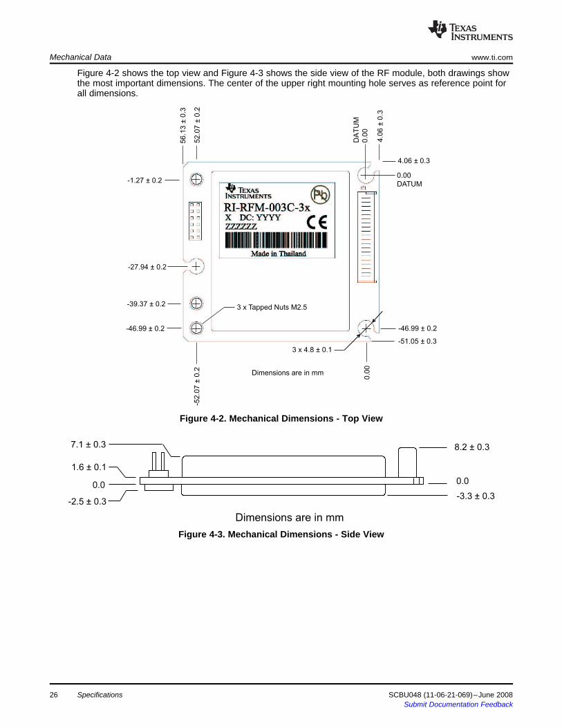
Figure 4-2 shows the top view and Figure 4-3 shows the side view of the RF module, both drawings showthe most important dimensions. The center of the upper right mounting hole serves as reference point forall dimensions.
Figure 4-2. Mechanical Dimensions - Top View
Figure 4-3. Mechanical Dimensions - Side View
26 Specifications SCBU048 (11-06-21-069)–June 2008Submit Documentation Feedback

Chapter 5SCBU048 (11-06-21-069)–June 2008
Installation and Use
This chapter provides the specific details that you will need to install the TI Mini-RFM correctly. It includesa detailed description of the power supply requirements, the antenna characteristics, the connecting cableand how to tune the antenna to resonance.
Topic .................................................................................................. Page
5.1 Mechanical Mounting................................................................. 285.2 Supply Voltage ......................................................................... 285.3 Receiver Signal Strength Output RXSS-....................................... 305.4 Programming a Transponder...................................................... 315.5 Antenna Requirements .............................................................. 325.6 Antenna Tuning ........................................................................ 33
SCBU048 (11-06-21-069)–June 2008 Installation and Use 27Submit Documentation Feedback

5.1 Mechanical Mounting
5.2 Supply Voltage
Mechanical Mounting www.ti.com
To protect the RF module from strong mechanical shock and vibration, grommets are inserted into themounting hole of the PCB as shown in Figure 5-1. Because the grommets are made of soft material,eyelets or spacers must be inserted into them when the RF module is mounted with screws.
Figure 5-1. PCB Mounting Proposal
Note: Take care when disconnecting ST1 that you pull the plug straight out and do not apply anysideways strain to the plastic guides.
The module uses two different supply lines each with a separate ground line. The receiver and the logicare supplied via the VSRL and GNDL pins from a voltage regulated power supply. The transmitter powerstage with its relatively high current consumption is supplied via the VSP and GNDP pins. The supplyvoltage range for VSP is wider than for VSL. This allows the direct connection of VSP to a four cell NiCdbattery, if the variation of the power pulse field strength caused by the variation of the battery voltage isacceptable.
Both ground lines GNDL and GNDP are decoupled inside the RFM with the resistor R_GND and thecapacitor C_GND and have to be connected together externally as shown in Figure 5-2 or Figure 5-3(depending on your power supply). This technique allows the power ground level GNDP to float in acertain range against the logic ground level GNDL without creating adverse effects to the control signalsfrom and to the control unit. Floating GNDP can happen during transmit time if you are using a long supplyline between the RF module and a control module.
Figure 5-2 shows an example of how to supply the RF module in a battery supplied reading unit whereshort lines are possible.
Figure 5-3 shows an example of how to wire a stationary application where long supply lines (over 15 cm)are used. The capacitor C_E1 between the VSP and GNDP pins is necessary to reduce the RF ripplevoltage and EMI on the supply line and must have low impedance at the transmit frequency (ESR =Equivalent Serial Resistor). In addition the common mode choke coil (choke) and the capacitor C_E2 alsoreduce the EMI during transmit time. These components should be placed as closely as possible to theRF module connector ST1.
28 Installation and Use SCBU048 (11-06-21-069)–June 2008Submit Documentation Feedback

www.ti.com Supply Voltage
The capacitor values shown in Figure 5-2 and Figure 5-3 are for general use and can vary according todifferent application requirements.
Regardless of which kind of power supply you use, we recommend that you build in fuses or electroniccurrent limitations in between the RF module and the power supplies to avoid any damage in case of shortcircuit. The value of the fuse depends very much on the application, for example: the current consumptionof the module which in turn depends on several factors, such as: the antenna used, whether or not acapacitor is connected and its size.
Note: The fuse load for VSP under normal conditions is less than 1 A.
If the Mini-RFM is connected into an application where the power is permanently on (hotconnecting), the load could surge by several amps due to the current in capacitor CS1 insidethe Mini-RFM.
Figure 5-2. Supply Line Wiring for Short Supply Lines
Figure 5-3. Supply Line Wiring for a Separated Power Supply
SCBU048 (11-06-21-069)–June 2008 Installation and Use 29Submit Documentation Feedback

5.3 Receiver Signal Strength Output RXSS-
Receiver Signal Strength Output RXSS- www.ti.com
If you are going to operate more than one TI reader in a local area, the systems should be synchronizedto each other. An intelligent control unit achieves this synchronization by sampling for the presence orabsence of the field strength indicator signal RXSS-. A power pulse in the area will cause RXSS- to beactive. If the signal RXSS- is present the control unit ensures that the RF module transmits eithersimultaneously or sequentially to any other RFMs in the area.
The RXSS- output switches to low if the received signal strength exceeds the internal reference level. Thisreference level can be adjusted with the two receiver signal strength control inputs RSCA and RSCB.
Figure 5-4 and Figure 5-5 show the basic schematic of the signal strength indicator and two methods ofadjusting the switching level.
The circuit shown in Figure 5-4 works as a simple D/A converter where the digital inputs RSCA and RSCBare switched either to the ground GNDL or to the supply voltage VSRL. Because of the high inputimpedance of RSCA and RSCB, the switches can be replaced by computer controlled outputs. Such acircuit can adjust the sensitivities in four steps. A fifth step is given if both inputs are open.
Figure 5-4. Synchronization Output Control - Digital Adjustment
An analog adjustment of the sensitivity level can be realized if a potentiometer is used as shown inFigure 5-5 or if a variable voltage source is used to bias one or both of the control inputs RSCA andRSCB.
30 Installation and Use SCBU048 (11-06-21-069)–June 2008Submit Documentation Feedback

5.4 Programming a Transponder
www.ti.com Programming a Transponder
Figure 5-5. Synchronization Output Control - Analog Adjustment
To write data to a read/write transponder the transmitter of the RF module must be switched off and onperiodically after the power pulse is completed. As shown in Figure 5-6 each data bit has the same lengtht_bit, but the duration t_offL or t_offH during which the transmitter is switched off, determines the value ofthe bit. Because the antenna circuit of the module and the connected antenna form a resonance circuitwith a specific rise and fall characteristic of the resonance voltage, different RF module and antennacombinations might need different t_offL and t_offH timing. The values t_offL and t_offH shown insection 4.3 Timing Characteristics are the times applied to TXCT-. A high Q antenna such asRI-ANT-P02A is used.
Figure 5-6. Write Pulse Timing for TXCT-
A detailed description of the complete programming sequence is given in the Sequence Control Manual(document number 11-06-21-049).
SCBU048 (11-06-21-069)–June 2008 Installation and Use 31Submit Documentation Feedback

5.5 Antenna RequirementsAntenna Requirements www.ti.com
The antenna for a TI RF module is a coil with the inductance L_ANT and the Q-factor Q_ANT. To ensurethat the antenna can be tuned to resonance with the tuning capacitors inside the RF Module, theinductance L_ANT for an air coil antenna can vary in the limits given below:• L_ANT = 115 to 117 H (at f=134.2 kHz, V=1V)• Q_ANT = 200 or better is recommended for good read/write range.
Some factors that influence each other, are listed below.a. The size and the construction of the antenna coil is a key factor for the generated magnetic field
strength. The larger the area of an air coil antenna or the longer a ferrite core antenna is, the higherthe field strength for a given RFM set-up and a given Q-factor of the antenna coil.
b. The quality factor of the antenna coil is a parameter indicating its efficiency. The quality depends onthe construction and the wire used for the coil. Because of the high frequency, litze-wire is needed fora high Q-factor. The higher the Q-factor of the antenna coil the more energy can be “pulled” from theRF module for a given RF module set-up. If an antenna with ferrite core is used, it must be kept inmind that it may have a very high quality factor under test conditions, but the quality factor will drop if ahigh magnetic field is applied to the ferrite core.
c. A very important factor for a good read/write range is the correct orientation / polarization between thetransponder antenna and the antenna of the read/write unit.
d. Noise, i.e. magnetic interference energy in or close to the TI frequency range can reduce the readrange remarkably. Sources of interference can be, for example: electronic equipment with built-inswitch mode power supplies, monitors and TV-sets with their magnetic deflection, which are notshielded enough. In such conditions you may be able to obtain better read/write ranges with a smallerantenna rather than a large one. The reason for this is that a large antenna collects signals within alarger area and therefore produces a stronger interference signal compared with the relatively smalltransponder signal. Under some conditions, charging and/or writing to the transponder worksexcellently, but the reading unit cannot detect the transponder signal.
Figure 5-7 shows the dimensions of the ferrite stick antenna RI-ANT-P02A available for the RF ModuleRI-RFM-003C.
32 Installation and Use SCBU048 (11-06-21-069)–June 2008Submit Documentation Feedback

5.6 Antenna Tuning
5.6.1 To Switch On the Transmitter
5.6.2 To Tune the Antenna Circuit
www.ti.com Antenna Tuning
Figure 5-7. Stick Antenna RI-ANT-P02A
To get all the available field strength from the antenna, it must be tuned to resonance. To do this, thefollowing set-up and equipment are required.
The reading/writing unit or test set up should be able to switch the RF module’s transmitter to a fastrepeating reading mode or continuous wave mode. If a continuous wave mode is applied, care must betaken not to exceed the duty cycle limitation as given in section 4.3. Time when the transmitter is switchedon but during which the current consumption is less than I_VSPcont, does not add to the duty cycle.
The built-in tuning capacitors C_AT1 to C_AT6, which are available at ST2, should be used to tune theresonance frequency of the antenna circuit to the output frequency of the transmitter. The most simplemethod of tuning is to use a switch box connected to the antenna tuning connector ST2; this will allow thecapacity of the antenna resonant circuit to be increased by connecting the built-in tuning capacitors to theground.
The switch box in its simplest version is an array of six well isolated, high voltage proof ON/OFF switches,which are connected to the antenna tuning connector ST2 (Antenna Tuning Switch Box RI-ACC-ATS1).
If you have to tune a lot of Mini-RFMs (for example on a production run) it would be helpful to build acomputer (or electronically) controlled tuning box that allows you to start the tuning procedure and then setthe jumpers according to the result of the tuning. The cable from the switch box to the connector ST2should be as short as possible (less that 20 cm) in order to get the same tuning results as with thejumpers.
SCBU048 (11-06-21-069)–June 2008 Installation and Use 33Submit Documentation Feedback

5.6.3 To Detect the Correct Tuning
5.6.4 Tuning Procedure
Antenna Tuning www.ti.com
There are two basic methods to detect the correct tuning point, they are:• Method 1: Tune the antenna circuit to maximum current consumption of the transmitter power stage by
inserting a current meter into the VSP-line which is an easy way for production. The lines of the metershould be as short as possible, or they must be RF decoupled close to the RF module.
• Method 2: Tune the antenna circuit to the maximum of the magnetic field strength generated by theantenna.
WARNINGCARE MUST BE TAKEN WHEN HANDLING THE MINI-RFM. HIGHVOLTAGE ACROSS THE ANTENNA TERMINALS AND TUNINGCONNECTORS COULD BE HARMFUL TO YOUR HEALTH. IF THEANTENNA INSULATION IS DAMAGED, IT MUST NOT BECONNECTED TO THE MINI-RFM.
Ensure that the reader is switched OFF.
Connect the antenna to the RF Module.
Remove all jumpers from the tuning connector ST2, and connect the switch box with all six switches in theOFF position.
Switch the RF module transmitter ON (continuous or fast reading mode).
While watching the current meter, increase tuning capacity with the switch box step-by-step until you finda peak.
Note: If you are using a switch box, do not forget that the capacitors attached to the jumpers arebinary weighted, and you should set the switches in a binary way:
Switch 1 ONSwitch 1 OFF Switch 2 ONSwitch 1 ON Switch 2 ONSwitch 1 OFF Switch 2 OFF Switch 3 ONand so on.
When you find a peak, continue with two more steps and check in case you find another higher peak.Looking for a possible second peak is necessary because the capacitors of the tuning network haveoverlapping capacitance, which causes discontinuous capacitance steps.
Check if the power stage supply current or the field strength has the correct value for that application.
Switch the transmitter OFF, disconnect the switch box and then plug-in jumpers at all the places where theswitches are in the ON position.
Switch ON the equipment again and check if the current or field strength are almost the same as theywere with the switch box connected.
Switch OFF the transmitter or reading unit. Tuning is completed.
34 Installation and Use SCBU048 (11-06-21-069)–June 2008Submit Documentation Feedback

Chapter 6SCBU048 (11-06-21-069)–June 2008
Warnings, Cautions, and Notices
This chapter provides the Warnings, Cautions and Notices that are relevant to the Mini-RFM.
Topic .................................................................................................. Page
6.1 FCC/Telecommunications Regulations ........................................ 366.2 Important Note to Purchasers/Users of the Mini-RFM in the USA .... 366.3 Warning ................................................................................... 366.4 Cautions .................................................................................. 36
SCBU048 (11-06-21-069)–June 2008 Warnings, Cautions, and Notices 35Submit Documentation Feedback

6.1 FCC/Telecommunications Regulations
6.2 Important Note to Purchasers/Users of the Mini-RFM in the USA
6.3 Warning
6.4 Cautions
FCC/Telecommunications Regulations www.ti.com
The TI RF Module generates RF emissions at 134.2 kHz. The radiation of the fundamental and theharmonics will vary with the type of antenna and other devices or functions connected to the RF module.
The required FCC or Telecommunications approvals must be obtained prior to operating the TI RF Modulewith antenna(s), power supply and a control module or other devices.
Sale, lease or operation in other countries may be subject to prior approval by the government or otherorganizations.
The TI RF Module product is considered by the Federal Communications Commission (FCC) to be asubassembly. As such, no prior approval is required to import, sell or otherwise market the RF Module inthe United States. In order to form a functioning radio frequency RF device, the RF Module must beconnected to a suitable antenna, power supply, and control circuitry. A radio frequency device may not beoperated unless authorized by the FCC nor may a radio frequency device be marketed (i.e. sold, leased,imported, or advertised for sale or lease) without the prior grant of an FCC equipment authorization.
FCC authorization to operate an RF device may take one of two forms: first, the FCC may grant the useran experimental license; second, the FCC may issue an equipment authorization permitting use of the RFdevice on an unlicensed basis. TI can assist the user in obtaining an experimental license that will cover aspecific installation of the RF Module in a specific site or sites. Experimental authorizations areappropriate to cover operations during the development of an RF device. A grant of equipmentauthorization (known as certification) must be obtained from the FCC before RF devices are marketed oroperated on a nondevelopment basis.
An equipment authorization has already been issued for use of the RF Module and other TI equipment(including antennas) in certain configurations. This authorization does not cover all possible combinationsof equipment and, in particular, covers only specific antenna configurations. Should a user desire to usethe RF Module in a configuration not yet approved, TI can assist that customer to obtain the necessaryequipment approval.
Care must be taken when handling the RF Module. High voltage across the antenna terminals and tuningconnector could be harmful to your health. If the antenna insulation is damaged it should not be connectedto the RF Module.
The RF Module might be subject to damage by electrostatic discharge (ESD) and should therefore only behandled by ESD protected personnel at ESD secured workplaces.
The transmitter power output stage can be damaged, if the antenna terminal A1 has a short circuit eitherto the ground or to the supply voltage and no current limitation is applied.
The transmitter power output stage can operate only with a limited duty cycle. This subject needs to begiven attention especially during the antenna tuning procedure.
The ground pins GNDL and GNDP have to be connected externally to avoid damage to the RF Module.
36 Warnings, Cautions, and Notices SCBU048 (11-06-21-069)–June 2008Submit Documentation Feedback

IMPORTANT NOTICETexas Instruments Incorporated and its subsidiaries (TI) reserve the right to make corrections, modifications, enhancements, improvements,and other changes to its products and services at any time and to discontinue any product or service without notice. Customers shouldobtain the latest relevant information before placing orders and should verify that such information is current and complete. All products aresold subject to TI’s terms and conditions of sale supplied at the time of order acknowledgment.TI warrants performance of its hardware products to the specifications applicable at the time of sale in accordance with TI’s standardwarranty. Testing and other quality control techniques are used to the extent TI deems necessary to support this warranty. Except wheremandated by government requirements, testing of all parameters of each product is not necessarily performed.TI assumes no liability for applications assistance or customer product design. Customers are responsible for their products andapplications using TI components. To minimize the risks associated with customer products and applications, customers should provideadequate design and operating safeguards.TI does not warrant or represent that any license, either express or implied, is granted under any TI patent right, copyright, mask work right,or other TI intellectual property right relating to any combination, machine, or process in which TI products or services are used. Informationpublished by TI regarding third-party products or services does not constitute a license from TI to use such products or services or awarranty or endorsement thereof. Use of such information may require a license from a third party under the patents or other intellectualproperty of the third party, or a license from TI under the patents or other intellectual property of TI.Reproduction of TI information in TI data books or data sheets is permissible only if reproduction is without alteration and is accompaniedby all associated warranties, conditions, limitations, and notices. Reproduction of this information with alteration is an unfair and deceptivebusiness practice. TI is not responsible or liable for such altered documentation. Information of third parties may be subject to additionalrestrictions.Resale of TI products or services with statements different from or beyond the parameters stated by TI for that product or service voids allexpress and any implied warranties for the associated TI product or service and is an unfair and deceptive business practice. TI is notresponsible or liable for any such statements.TI products are not authorized for use in safety-critical applications (such as life support) where a failure of the TI product would reasonablybe expected to cause severe personal injury or death, unless officers of the parties have executed an agreement specifically governingsuch use. Buyers represent that they have all necessary expertise in the safety and regulatory ramifications of their applications, andacknowledge and agree that they are solely responsible for all legal, regulatory and safety-related requirements concerning their productsand any use of TI products in such safety-critical applications, notwithstanding any applications-related information or support that may beprovided by TI. Further, Buyers must fully indemnify TI and its representatives against any damages arising out of the use of TI products insuch safety-critical applications.TI products are neither designed nor intended for use in military/aerospace applications or environments unless the TI products arespecifically designated by TI as military-grade or "enhanced plastic." Only products designated by TI as military-grade meet militaryspecifications. Buyers acknowledge and agree that any such use of TI products which TI has not designated as military-grade is solely atthe Buyer's risk, and that they are solely responsible for compliance with all legal and regulatory requirements in connection with such use.TI products are neither designed nor intended for use in automotive applications or environments unless the specific TI products aredesignated by TI as compliant with ISO/TS 16949 requirements. Buyers acknowledge and agree that, if they use any non-designatedproducts in automotive applications, TI will not be responsible for any failure to meet such requirements.Following are URLs where you can obtain information on other Texas Instruments products and application solutions:Products ApplicationsAmplifiers amplifier.ti.com Audio www.ti.com/audioData Converters dataconverter.ti.com Automotive www.ti.com/automotiveDSP dsp.ti.com Broadband www.ti.com/broadbandClocks and Timers www.ti.com/clocks Digital Control www.ti.com/digitalcontrolInterface interface.ti.com Medical www.ti.com/medicalLogic logic.ti.com Military www.ti.com/militaryPower Mgmt power.ti.com Optical Networking www.ti.com/opticalnetworkMicrocontrollers microcontroller.ti.com Security www.ti.com/securityRFID www.ti-rfid.com Telephony www.ti.com/telephonyRF/IF and ZigBee® Solutions www.ti.com/lprf Video & Imaging www.ti.com/video
Wireless www.ti.com/wireless
Mailing Address: Texas Instruments, Post Office Box 655303, Dallas, Texas 75265Copyright © 2008, Texas Instruments Incorporated


