31
Series Circuits ET 162 Circuit Analysis Electrical and Telecommunication Engineering Technology Professor Jang
| Date post: | 22-Dec-2015 |
| Category: |
Documents |
| View: | 233 times |
| Download: | 4 times |

Series Circuits
ET 162 Circuit Analysis
Electrical and Telecommunication Engineering Technology
Professor Jang
AcknowledgementAcknowledgement
I want to express my gratitude to Prentice Hall giving me the permission to use instructor’s material for developing this module. I would like to thank the Department of Electrical and Telecommunications Engineering Technology of NYCCT for giving me support to commence and complete this module. I hope this module is helpful to enhance our students’ academic performance.

OUTLINESOUTLINES Introduction to Series Circuits
ET162 Circuit Analysis – Series Circuits Boylestad 2
Kirchhoff’s Voltage Law
Interchanging Series Elements
Ideal dc Voltage Sources vs. Non-ideal Sources
Voltage Divider Rule
Series Circuits – Notation
Voltage Regulation
Key Words: Series Circuit, Kirchhoff’s Voltage Law, Voltage Divider Rule

Series Circuits - Introduction
Two types of current are available to the consumer today. One is direct current (dc), in which ideally the flow of charge (current) does not change in magnitude with time. The other is sinusoidal alternating current (ac), in which the flow of charge is continually changing in magnitude with time.
FIGURE 5.1 Introducing the basic components of an electric circuit.
V (volt) = E (volt)
ET162 Circuit Analysis – Series Circuits Boylestad 3

ET162 Circuit Analysis – Ohm’s Law and Series Current Floyd 4
Series Circuits
A circuit consists of any number of elements joined at terminal points, providing at least one closed path through which charge can flow.
Two elements are in series if
1.They have only one terminal in common2.The common point between the two points is not connected to another
current-carrying element.
FIGURE 5.2 (a) Series circuit; (b) situation in which R1 and R2 are not in series.
The current is the same through series elements.
The total resistance of a series circuit is the sum of the resistance levels
In Fig. 5.2(a), the resistors R1 and R2 are in series because they have only point b in common.

T
s RE
I
1
2
11
2
1111 R
VRIIVP
The total resistance of a series circuit is the sum of the resistance levels. In general, to find the total resistance of N resistors in series, the following equation is applied:
RT = R1 + R2 + R3 + · · ·+ RN
(amperes, A)
Pdel = E I
Pdel = P1 + P2 + P3 + · · · + PN
The total power delivered to a resistive circuit is equal to the total power dissipated by resistive elements.
V1 = I R1, V2 = I R2, V3 = I R3, · · ·VN = I RN
(volts, V)
(ohms, Ω)
FIGURE 5.3 Replacing the series resistors R1 and R2 of Fig. 5.2 (a) with the total resistance.
(watts, W)
(watts, W)
ET162 Circuit Analysis – Series Circuits Boylestad 5
ET162 Circuit Analysis – Ohm’s Law and Series Current Boylestad 6
AV
RE
IT
s 5.2820
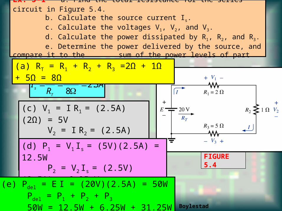
Ex. 5-1 a. Find the total resistance for the series circuit in Figure 5.4. b. Calculate the source current Is. c. Calculate the voltages V1, V2, and V3. d. Calculate the power dissipated by R1, R2, and R3. e. Determine the power delivered by the source, and compare it to the sum of the power levels of part (b).
(a) RT = R1 + R2 + R3 =2Ω + 1Ω + 5Ω = 8Ω
(c) V1 = I R1 = (2.5A)(2Ω) = 5V V2 = I R2 = (2.5A)(1Ω) = 2.5V V3 = I R3 = (2.5A)(5Ω) = 12.5V
(d) P1 = V1 Is = (5V)(2.5A) = 12.5W P2 = V2 Is = (2.5V)(2.5A) = 6.25 W P3 = V3 Is = (12.5V)(2.5A) = 31.25 W
(e) Pdel = E I = (20V)(2.5A) = 50W Pdel = P1 + P2 + P3
50W = 12.5W + 6.25W + 31.25W
FIGURE 5.4

Ex. 5-2 Determine RT, Is, and V2 for the circuit of Figure 5.5.
AV
RE
IT
s 22550
RT = R1 + R2 + R3 + R3 = 7Ω + 4Ω + 7Ω + 7Ω = 25Ω
V2 = Is R2 = (2A)(4Ω) = 8V Figure 5.5
Ex. 5-3 Given RT and I, calculate R1 and E for the circuit of Figure 5.6.
R R R R
k R k k
R k k k
E I R A V
T
T
1 2 3
1
1
3 3
1 2 4 6
1 2 1 0 2
6 1 0 1 2 1 0 7 2
Figure 5.6ET162 Circuit Analysis – Series Circuits Boylestad
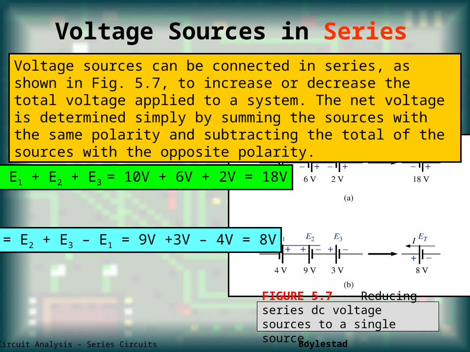
ET = E1 + E2 + E3 = 10V + 6V + 2V = 18V
ET = E2 + E3 – E1 = 9V +3V – 4V = 8V
FIGURE 5.7 Reducing series dc voltage sources to a single source.
Voltage Sources in SeriesVoltage sources can be connected in series, as shown in Fig. 5.7, to increase or decrease the total voltage applied to a system. The net voltage is determined simply by summing the sources with the same polarity and subtracting the total of the sources with the opposite polarity.
ET162 Circuit Analysis – Series Circuits Boylestad 8
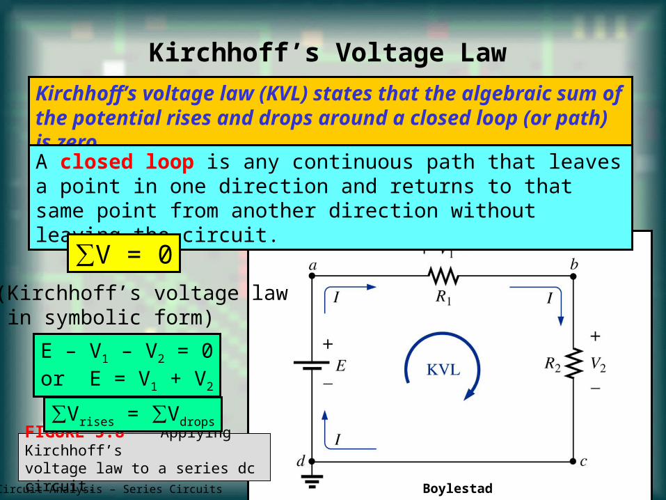
Kirchhoff’s Voltage Law
Kirchhoff’s voltage law (KVL) states that the algebraic sum of the potential rises and drops around a closed loop (or path) is zero.
A closed loop is any continuous path that leaves a point in one direction and returns to that same point from another direction without leaving the circuit.
∑V = 0
(Kirchhoff’s voltage law in symbolic form)
FIGURE 5.8 Applying Kirchhoff’s voltage law to a series dc circuit.
E – V1 – V2 = 0or E = V1 + V2
∑Vrises = ∑Vdrops
ET162 Circuit Analysis – Series Circuits Boylestad 9
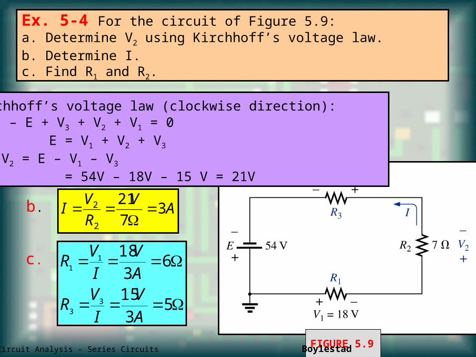
Ex. 5-4 For the circuit of Figure 5.9:a. Determine V2 using Kirchhoff’s voltage law.b. Determine I.c. Find R1 and R2.
b. AV
R
VI 3
7
21
2
2
53
15
63
18
33
11
AV
IV
R
AV
IV
Rc.
a. Kirchhoff’s voltage law (clockwise direction):– E + V3 + V2 + V1 = 0
or E = V1 + V2 + V3
and V2 = E – V1 – V3 = 54V – 18V – 15 V = 21V
FIGURE 5.9ET162 Circuit Analysis – Series Circuits Boylestad 10

Ex. 5-5 Find V1 and V2 for the network of Fig. 5.10.
2 5 1 5 0
4 01
1
V V V
and V V
For path 1, starting at point a in a clockwise direction:
For path 2, starting at point a in a clockwise direction:
V V
and V V2
2
2 0 0
2 0
FIGURE 5.10
ET162 Circuit Analysis – Series Circuits Boylestad 11

6 0 4 0 3 0 0
5 0
V V V V
and V Vx
x
Ex. 5-6 Using Kirchhoff’s voltage law, determine the unknown voltage for the network of Fig. 5.11.
6 1 4 2 0
1 8
V V V V
and V Vx
x
FIGURE 5.11
ET162 Circuit Analysis – Series Circuits Boylestad 12
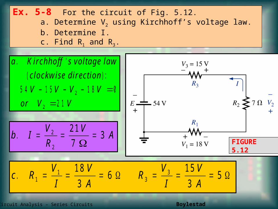
Ex. 5-8 For the circuit of Fig. 5.12.a. Determine V2 using Kirchhoff’s voltage law.b. Determine I.c. Find R1 and R3.
a K irchho ff s vo ltage law
clockw ise d irection
V V V V
or V V
. '
( ):
5 4 1 5 1 8 0
2 12
2
b IV
R
VA. 2
2
2 1
73
c RV
I
V
AR
V
I
V
A. 1
13
31 8
36
1 5
35
FIGURE 5.12
ET162 Circuit Analysis – Series Circuits Boylestad 13

Voltage Divider Rule (VDR)
The voltage across the resistive elements will divide as the magnitude of the resistance levels.
FIGURE 5.13 Revealing how the voltage will divide across series resistive elements.
FIGURE 5.14 The ratio of the resistive values determines the voltage division of a series dc circuit.
The voltages across the resistive elements of Fig. 5.13 are provided. Since the resistance level of R1 is 6 times that of R3, the voltage across R1 is 6 times that of R3. The fact that the resistance level of R2 is 3 times that of R1 results in three times the voltage across R2. Finally, since R1 is twice R2, the voltage across R1 is twice that of R2. If the resistance levels of all resistors of Fig. 5.13 are increased by the same amount, as shown in Fig. 5.14, the voltage levels will all remain the same.

The voltage divider rule (VDR) can be derived by analyzing the network of Fig. 5.15.
TT
TT
RER
RRE
IRV
RER
RRE
IRV
2222
1111
T
xx R
ERV
RT = R1 + R2
and I = E/RT
Applying Ohm’s law:
(voltage divider rule)
FIGURE 5.15 Developing the voltage divider rule.
ET162 Circuit Analysis – Series Circuits Boylestad 15

Ex. 5-9 Using the voltage divider rule, determine the voltages V1 and V3 for the series circuit of Figure 5.16.
V
VVkkk
Vk
RRRER
RER
T
615
901015
45102852
452
3
3
321
11
VV
V
k
Vk
R
ER
T
2415
3601015
45108
15
458
3
3
3
V1
V3
FIGURE 5.16
ET162 Circuit Analysis – Series Circuits Boylestad 16

Notation-Voltage Sources and Ground
Notation will play an increasingly important role on the analysis to follow. Due to its importance we begin to examine the notation used throughout the industry.
Except for a few special cases, electrical and electronic systems are grounded for reference and safety purposes. The symbol for the ground connection appears in Fig. 5.25 with its defined potential level-zero volts. FIGURE 5.25 Ground potential.
ET162 Circuit Analysis – Series Circuits-Notation Boylestad 2FIGURE 5.26 Three ways to sketch the same series dc circuit.
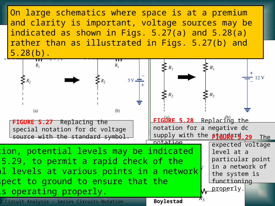
FIGURE 5.27 Replacing the special notation for dc voltage source with the standard symbol.
On large schematics where space is at a premium and clarity is important, voltage sources may be indicated as shown in Figs. 5.27(a) and 5.28(a) rather than as illustrated in Figs. 5.27(b) and 5.28(b).
FIGURE 5.28 Replacing the notation for a negative dc supply with the standard notation.
In addition, potential levels may be indicatedin Fig. 5.29, to permit a rapid check of the potential levels at various points in a networkwith respect to ground to ensure that the System is operating properly.
FIGURE 5.29 The expected voltage level at a particular point in a network of the system is functioning properly.
ET162 Circuit Analysis – Series Circuits-Notation Boylestad 18

Double-Subscript NotationThe fact that voltage is an across variable and exists between two points has resulted in a double-script notation that defined the first subscript as the higher potential.
In Fig. 5.30(a), the two points that define the voltage across the resistor R are denoted by a and b. Since a is the first subscript for Vab, point a must have higher potential than point b if Vab is to have a positive value. If point b is at a higher potential than point a, Vab will have a negative value, as indicated in Fig. 5.30(b). The voltage Vab is the voltage at point a with respect to point b.
ET162 Circuit Analysis – Series Circuits-Notation Floyd 19FIGURE 5.30 Defining the sign for double-subscript notation.
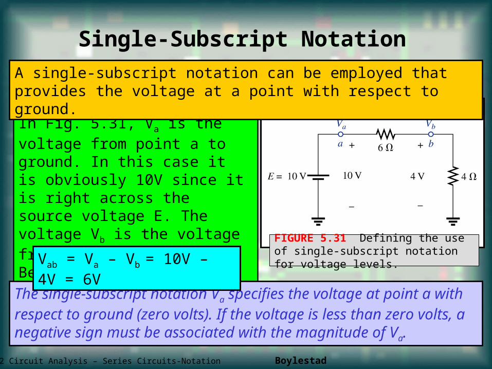
Single-Subscript Notation
In Fig. 5.31, Va is the voltage from point a to ground. In this case it is obviously 10V since it is right across the source voltage E. The voltage Vb is the voltage from point b to ground. Because it is directly across the 4-Ω resistor, Vb = 4V.
A single-subscript notation can be employed that provides the voltage at a point with respect to ground.
FIGURE 5.31 Defining the use of single-subscript notation for voltage levels.
The single-subscript notation Va specifies the voltage at point a with respect to ground (zero volts). If the voltage is less than zero volts, a negative sign must be associated with the magnitude of Va.
Vab = Va – Vb = 10V – 4V = 6V
ET162 Circuit Analysis – Series Circuits-Notation Boylestad 20

FIGURE 5.32 Example 5.14.
General CommentsA particularly useful relationship can now be established that will have extensive applications in the analysis of electronic circuits. For the above notational standards, the following relationship exists:
Vab = Va – Vb
Ex. 5-14 Find the voltage Vab for the conditions of Fig. 5.32.
V V V
V V
V
ab a b
1 6 2 0
4
ET162 Circuit Analysis – Series Circuits-Notation Boylestad 21

FIGURE 5.34
Ex. 5-15 Find the voltage Va for the configuration of Fig. 5.33.
V V V
V V V V V
V
ab a b
a ab b
5 4
9
V V V V V
V V Vab a b
2 0 1 5
2 0 1 5 3 5
( )
Ex. 5-16 Find the voltage Vab for the configuration of Fig. 5.34.
FIGURE 5.33
Floyd 8
FIGURE 5.35 The impact of positive and negative voltages on the total voltage drop.
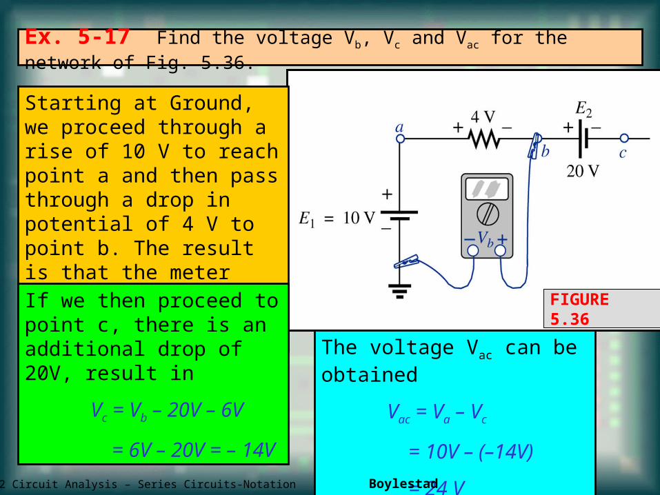
Ex. 5-17 Find the voltage Vb, Vc and Vac for the network of Fig. 5.36.
Starting at Ground, we proceed through a rise of 10 V to reach point a and then pass through a drop in potential of 4 V to point b. The result is that the meter will read
Vb = +10V – 4V = 6V
FIGURE 5.36If we then proceed to point c, there is an additional drop of 20V, result in
Vc = Vb – 20V – 6V
= 6V – 20V = – 14V
The voltage Vac can be obtained
Vac = Va – Vc
= 10V – (–14V)
= 24 VET162 Circuit Analysis – Series Circuits-Notation Boylestad 23
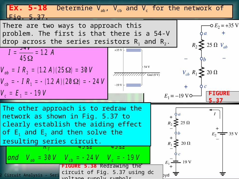
IE E
R
V V VA
and V V V V V VT
ab cb c
1 2 1 9 3 5
4 5
5 4
4 51 2
3 0 2 4 1 9
.
ET162 Circuit Analysis – Series Circuits Floyd 24
Ex. 5-18 Determine Vab, Vcb and Vc for the network of Fig. 5.37.
FIGURE 5.38 Redrawing the circuit of Fig. 5.37 using dc voltage supply symbols.
IV
A
V I R A V
V I R A V
V E V
ab
cb
c
5 4
4 51 2
1 2 2 5 3 0
1 2 2 0 2 4
1 9
2
1
1
.
( . )( )
( . )( )
The other approach is to redraw the network as shown in Fig. 5.37 to clearly establish the aiding effect of E1 and E2 and then solve the resulting series circuit.
There are two ways to approach this problem. The first is that there is a 54-V drop across the series resistors R1 and R2.
FIGURE 5.37
Redrawing the network with standard battery symbol will result in the network of Fig.5.40. Applying the voltage divider rule,
FIGURE 5.40
Ex. 5-19 Using the voltage divider rule, determine the voltages V1 and V2 for of Fig. 5.39.
VR E
R R
VV
VR E
R R
VV
11
1 2
22
1 2
4 2 4
4 21 6
2 2 4
4 28
( )( )
( )( )
FIGURE 5.39
ET162 Circuit Analysis – Series Circuits-Notation Boylestad 25

FIGURE 5.40
Ex. 5-20 For the network of Fig. 5.40: a. Calculate Vab.
b. Determine Vb. c. Calculate Vc.
a V oltage d ivider ru le
VR E
R
VVab
T
. :
( )( )
1 2 1 0
2 3 52
b V oltage d ivider ru le
V V VR R E
R
VV
or V V V E V
V V V
b R RT
b a ab ab
. :
( )
( )( )
2 3
2 3
3 5 1 0
1 08
1 0 2 8
c. Vc = ground potential = 0 V
ET162 Circuit Analysis – Series Circuits-Notation Boylestad 26

Every source of voltage, whether a generator, battery, or laboratory supply as shown in Fig. 5.41(a), will have some internal resistance (know as the non-ideal voltage source). The equivalent circuit of any source of voltage will therefore appear as shown in Fig. 5.41(b).
FIGURE 5.41 (a) Sources of dc voltage; (b) equivalent circuit.
Ideal Voltage Sources vs. Non-ideal Voltage Sources
ET162 Circuit Analysis – Series Circuits-Notation Boylestad 27

In all the circuit analyses to this point, the ideal voltage source (no internal resistance) was used shown in Fig. 5.42(a). The ideal voltage source has no internal resistance and an output voltage of E volts with no load or full load. In the practical case [Fig. 5.42(b)], where we consider the effects of the internal resistance, the output voltage will be E volts only when no-load (IL = 0) conditions exist. When a load is connected [Fig. 5.42(c)], the output voltage of the voltage source will decrease due to the voltage drop across the internal resistance.
FIGURE 5.42 Voltage source: (a) ideal, Rint = 0 Ω; (b) Determining VNL; (c) determining Rint.
ET162 Circuit Analysis – Series Circuits-Notation Boylestad 28
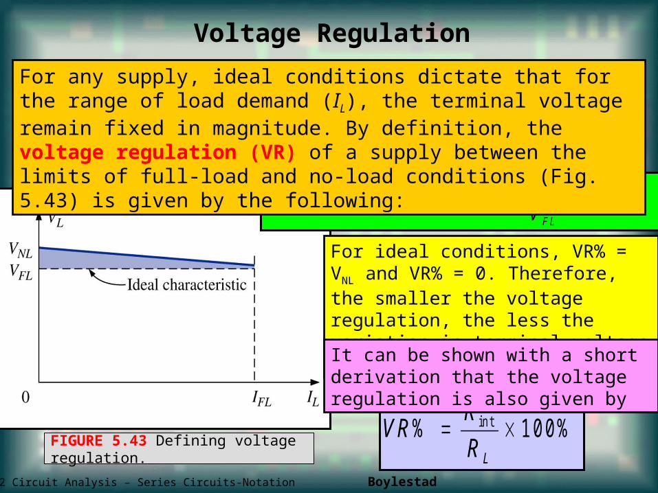
V oltage regu la tion V RV V
VN L F L
F L
( )%
1 0 0 %
V RR
R L
% in t 1 0 0 %FIGURE 5.43 Defining voltage regulation.
Voltage Regulation
For any supply, ideal conditions dictate that for the range of load demand (IL), the terminal voltage remain fixed in magnitude. By definition, the voltage regulation (VR) of a supply between the limits of full-load and no-load conditions (Fig. 5.43) is given by the following:
For ideal conditions, VR% = VNL and VR% = 0. Therefore, the smaller the voltage regulation, the less the variation in terminal voltage with change in load.
It can be shown with a short derivation that the voltage regulation is also given by
ET162 Circuit Analysis – Series Circuits-Notation Boylestad 29
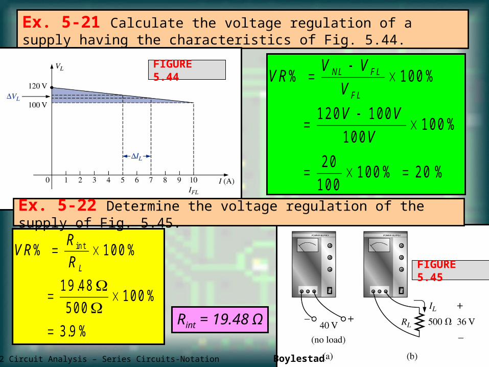
Ex. 5-21 Calculate the voltage regulation of a supply having the characteristics of Fig. 5.44.
V RV V
V
V V
V
N L F L
F L
% %
%
% %
1 0 0
1 2 0 1 0 0
1 0 01 0 0
2 0
1 0 01 0 0 2 0
V RR
R L
% %
.%
. %
in t
1 0 0
1 9 4 8
5 0 01 0 0
3 9
FIGURE 5.44
FIGURE 5.45
Ex. 5-22 Determine the voltage regulation of the supply of Fig. 5.45.
Rint = 19.48 Ω
ET162 Circuit Analysis – Series Circuits-Notation Boylestad 30


