This manual is intended for use by experienced techni-cians familiar with similar types of commercial grade com-munications equipment. It contains all required service in-formation for the equipment and is current as of the publica-tion data. Changes which may occur after publication arecovered by either Service Bulletins or Manual Revisions.These are issued as required.
ORDERING REPLACEMENT PARTSWhen ordering replacement parts or equipment informa-
tion, the full part identification number should be included.This applies to all parts : components, kits, or chassis. If thepart number is not known, include the chassis or kit numberof which it is a part, and a sufficient description of the re-quired component for proper identification.
PERSONNEL SAFETYThe following precautions are recommended for person-
nel safety :• DO NOT transmit if someone is within two feet (0.6
meter) of the antenna.• DO NOT transmit until all RF connectors are verified se-
cure and any open connectors are properly terminated.• SHUT OFF and DO NOT operate this equipment near
electrical blasting caps or in an explosive atmosphere.• All equipment should be properly grounded before
power-up for safe operation.• This equipment should be serviced by a qualified techni-
cian only.
PRE-INSTALLATION CONSIDERATIONS
1. UNPACKING
Unpack the radio from its shipping container and checkfor accessory items. If any item is missing, please contactKENWOOD immediately.
2. LICENSING REQUIREMENTS
Federal regulations require a station license for each ra-dio installation (mobile or base) be obtained by the equip-ment owner. The licensee is responsible for ensuring trans-mitter power, frequency, and deviation are within the limitspermitted by the station license.
Transmitter adjustments may be performed only by a li-censed technician holding an FCC first, second or generalclass commercial radiotelephone operator’s license. Thereis no license required to install or operate the radio.
GENERAL
3. PRE-INSTALLATION CHECKOUT
3-1. Introduction
Each radio is adjusted and tested before shipment. How-ever, it is recommended that receiver and transmitter opera-tion be checked for proper operation before installation.
3-2. Testing
The radio should be tested complete with all cabling andaccessories as they will be connected in the final installa-tion. Transmitter frequency, deviation, and power outputshould be checked, as should receiver sensitivity, squelchoperation, and audio output. Signalling equipment operationshould be verified.
4. PLANNING THE INSTALLATION
4-1. General
Inspect the vehicle and determine how and where theradio antenna and accessories will be mounted.
Plan cable runs for protection against pinching or crush-ing wiring, and radio installation to prevent overheating.
4-2. Antenna
The favored location for an antenna is in the center of alarge, flat conductive area, usually at the roof center. Thetrunk lid is preferred, bond the trunk lid and vehicle chassisusing ground straps to ensure the lid is at chassis ground.
4-3. Radio
The universal mount bracket allows the radio to bemounted in a variety of ways. Be sure the mounting surfaceis adequate to support the radio’s weight. Allow sufficientspace around the radio for air cooling. Position the radioclose enough to the vehicle operator to permit easy accessto the controls when driving.
4-4. DC Power and wiring
1. This radio may be installed in negative ground electricalsystems only. Reverse polarity will cause the cable fuseto blow. Check the vehicle ground polarity before installa-tion to prevent wasted time and effort.
2. Connect the positive power lead directly to the vehiclebattery positive terminal. Connecting the Positive lead toany other positive voltage source in the vehicle is not rec-ommended.
3. The cable provided with the radio is sufficient to handlethe maximum radio current demand. If the cable must beextended, be sure the additional wire is sufficient for thecurrent to be carried and length of the added lead.
3
TK-6110GENERAL / SYSTEM SET-UP
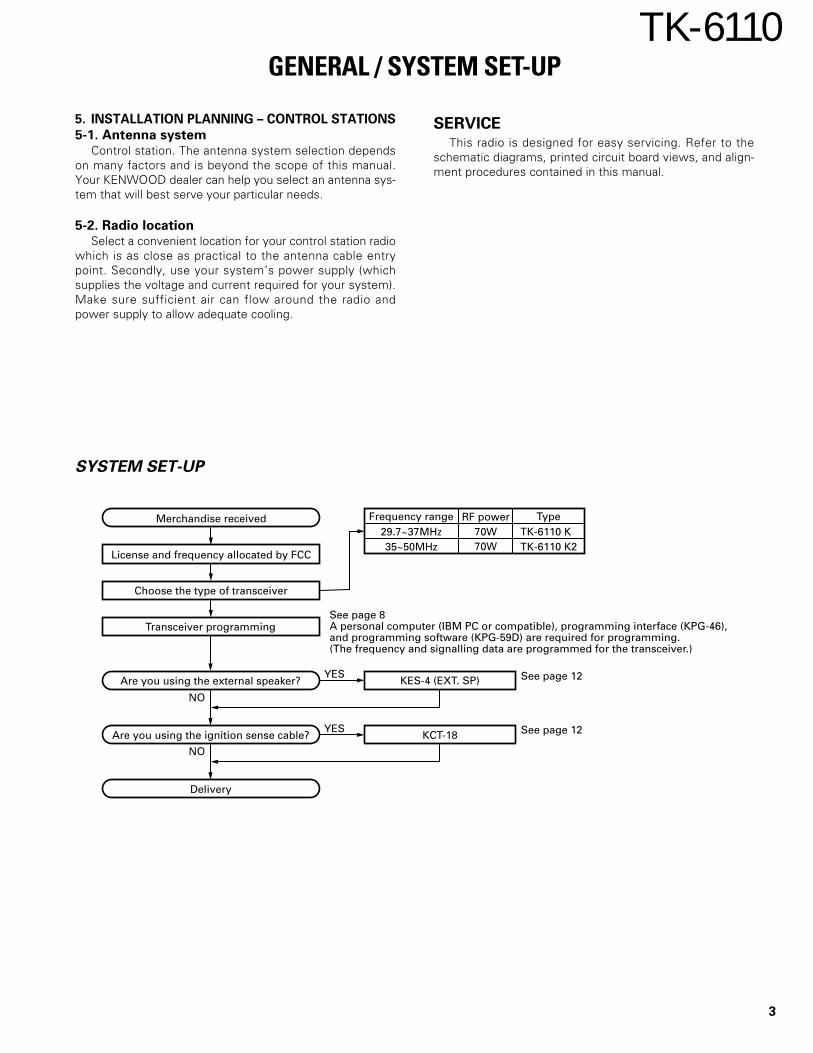
Merchandise received
License and frequency allocated by FCC
Choose the type of transceiver
Transceiver programming
Are you using the external speaker?
Are you using the ignition sense cable?
Delivery
NO
NO
KES-4 (EXT. SP)YES
KCT-18YES
See page 12
See page 12
See page 8A personal computer (IBM PC or compatible), programming interface (KPG-46),and programming software (KPG-59D) are required for programming.(The frequency and signalling data are programmed for the transceiver.)
Frequency range29.7~37MHz35~50MHz
RF power70W70W
TK-6110 KTK-6110 K2
Type
5. INSTALLATION PLANNING – CONTROL STATIONS
5-1. Antenna system
Control station. The antenna system selection dependson many factors and is beyond the scope of this manual.Your KENWOOD dealer can help you select an antenna sys-tem that will best serve your particular needs.
5-2. Radio location
Select a convenient location for your control station radiowhich is as close as practical to the antenna cable entrypoint. Secondly, use your system’s power supply (whichsupplies the voltage and current required for your system).Make sure sufficient air can flow around the radio andpower supply to allow adequate cooling.
SERVICEThis radio is designed for easy servicing. Refer to the
schematic diagrams, printed circuit board views, and align-ment procedures contained in this manual.
SYSTEM SET-UP
4
TK-6110
1. Controls and Functions
1-1. Front Panel
OPERATING FEATURES
MON A B C SCN
1
3 4 5 6 7 8 9 10
Display 2 Speaker
Volume controlTurn clockwise to increase the volume. Turn counter-
clockwise to decrease the volume.
/ keysPress these keys to activate their programmable func-
tions. The default settings of these keys are “Channel Up”( ) and “Channel Down” ( ).
Microphone jackInsert the microphone plug into this jack.
IO (Power) switchPress to switch the power ON. Press and hold for ap-
proximately 1 second to switch the power OFF.
MON keyPress MON to activate its programmable function. The
default setting of this key is “Monitor”.
A key
B key
C key
SCN keyPress SCN to activate its programmable function. The
default setting of this key is “Scan”.
LEDLights red while transmitting. Lights green while the se-
lected channel is busy. Blinks orange when you receive acall by 2-Tone or DTMF.
1
2
3
4
5
6
7
8
9
Press these PF (programmable function)keys to activate their programmable func-tions. The default setting of these keys is“No Function”.
10
1-2. Display
Displays the operating Channel number,the Channel name, and the transceiverstatus.Displays the operating channel numberand the channel status:P indicates a Priority channelHC indicates a Home ChanneltA indicates Talk Around modeFlashes when a call is received by DTMFor 2-Tone signaling. Appears during andafter transmitting if set by the dealer.Appears when signaling squelch isturned OFF.Appears while scanning is in progress.
Appears when the optional scramblerboard is enabled.Appears when the selected channel is inthe scanning sequence.Appears when Aux is ON.
Appears when Operator Selectable Toneis enabled.
1-3. Rear Panel
1-4. Microphone
TK-6110
Antennaconnector
Power inputconnector
15 pin connector(for accessories)
PTT (Push To Talk) switchPress and hold to transmit, then speak into the microphone. Release to receive.
5
TK-6110
2. Scanning
2-1. Start Scanning
You can start scanning when 1 priority channel and atleast 1 ADD channel, or 2 or more ADD channels are se-lected. The transceiver must be in the normal receivingmode (releasing PTT).
Press the key programmed to the scan, the scan starts.The “SCN” (scan) icon appears on the main display and“SCAN” or revert channel appears on the 8-digit alphanu-meric display.
2-2. Stop Scanning
The scan stops temporarily if the following conditions aresatisfied.1) A carrier is detected, then signalling matches on channel
for which receive the signalling is set by the program-ming software.
2) A carrier is detected on the channel for which receivingsignalling is not set by the programming software orwhen the monitor (signalling cancel) function is activated.
2-3. Types of Scan Channel
1) Priority channel is the most important channel for thescan, and always detects a signal during scan and whenthe scan stops temporarily.
2) Non-priority channels detects a signal during scan andwhen scan stops temporarily.
2-4. Setting Priority Channel
Priority channel can be set as follows with the program-ming software (KPG-59D).1) Specify priority channel as fixed priority channel.2) Make selected channels, priority channels.
2-5. Scan Type Depending on the Priority Channel
1) When no priority channels are set : Only the non-prioritychannels are scanned.If the transceiver stops on a non-priority channel, prioritychannel is still checked for signals at the specified timeintervals.If the transceiver detects a signal on a priority channel, itpauses at the priority channel and starts receiving thecalls.
2) When priority channel is set : Either priority channel isscanned.If a priority channel stops temporarily, it stops until thereis no signal on the priority channel.
2-6. Revert Channel
The revert channel is used to transmit during scanningand set by the programming software (KPG-59D).1) Last called channel
The transceiver reverts to the last called channel duringthe scan.
2) Last used channelThe transceiver reverts to the last used (transmitted)channel during scan. “Last used” revert channel in-cludes talkback function.
3) Selected with talkbackThe transceiver reverts to the channel before scanning orthe channel that you changed during scan.
4) Selected channelThe transceiver reverts to the channel before scanning orthe channel that you changed during scan.While the transceiver pauses scanning, the revert chan-nel becomes the channel you selected with [CH UP], [CHDW], [CH1] to [CH5] in the last step.
5) Priority with talkbackThe transceiver reverts to the priority channel.If you press PTT during a resume timer (dropout delaytime, TX dwell time) or calling, you can transmit on cur-rent channel to answer to the call however revert channelis set to priority channel.After resume time, scan re-starts and transmission chan-nel is return to priority channel.
6) PriorityThe transceiver reverts to the priority channel.
2-7. Scan End
When you press the key once again, programmed to thescan function during scan mode, the scan ends.
The scan icon “SCN” and “SCAN” or revert channel (pro-grammable) display goes off.
2-8. Temporarily Delete/Add
It is possible to delete or add channel temporarily duringscan. When scan stops on unnecessary channel for ex-ample by interference of the other party, activate the delete/add function (for example press the key), then that channelis deleted temporarily and scan re-start immediately.
When you would like to add the deleted channel tempo-rarily to scan sequence, select the desired (deleted) channelduring scan, activate the delete/add function (for examplepress the key) before scan re-start.
That channel is added temporarily to scan sequence. Thetemporary deleted or added channels are returns to pre-setdelete/add, when the transceiver exits from scan mode.
3. Optional FeaturesYou can use these features using the programming soft-
ware (KPG-59D).
3-1. Beep Tones
The beep tones (power on tone, control tone, warningtone, alert tone) are individually programmable to the fixedlevel 0 to 31 or follow the mechanical volume position.
3-2. Minimum Volume
The minimum volume is programmable (0 to 31). Thetransceiver remains the minimum volume level however themechanical volume position is set to zero.
3-3. BCL (Busy Channel Lockout) Override
You can transmit in spite of Busy Channel Lockout situa-tion. For example : To make an emergency voice call.
To transmit under busy channel lockout situation, pressPTT once more within approx. 500ms after the PTT release.
OPERATING FEATURES
6
TK-6110
3-4. Sub LCD Display
You can use 3-digit 7-segment the display to display thechannel number. It is useful when the main (8-digit 13-seg-ment) display indicates channel name.
3-5. Emergency Channel Display
The transceiver can be programmed to display “EMER-GENCY” channel name when it is in emergency mode.
If you set to “off” by KPG-59D the transceiver showsselected group/channel/status before entering to the emer-gency mode however the transceiver is in an emergencymode.
3-6. Clear to Transpond
The transceiver waits the transpond of 2-Tone/DTMF ifchannel is busy until channel open. This feature replies tothe transpond signal when the caller returns to receive.
3-7. Mode (Enable/Disable)
The transceiver has many special modes mainly for main-tenance.
· Panel Test mode· Clone mode· Main programming modeIt is possible to set enable/disable for each mode. We
recommend to set these mode to Disable after set up tosave contents.
3-8. ID
The transceiver is capable to have ID. The format isDTMF. The timing that the transceiver sends ID is program-mable.
Begin of TX : Connect ID is send on beginning of trans-mission.End of TX : Disconnect ID is send on end of transmission.Both : Connect ID is send on beginning of transmissionand disconnect ID is send on end of transmission.Off : Sending ID function is disabled.There is also “PTT ID” setting for each channel. Refer
“PTT ID” of channel feature.
3-9. OST (Operator Selectable Tone)
The transceiver is capable to have “OST” function and 16tone pair (QT/DQT) with max 8-digit name for each tone pair.
• “OST” Back Up
The transceiver is programmable the selected “OST”code is memorized or not. If you set to Disable (no memo-rized), the “OST” function always starts at “off”.
3-10. “TOT” (Time-Out Timer)
The transceiver has the “TOT”. This parameter selectsthe period of time users can continuously transmit.
When the selected period passes, the transceiver gener-ates an warning tone and stops the transmission.
3-11. “TOT” Pre-Alert
The transceiver has “TOT” pre-alert timer. This param-eter selects the time at which the transceiver generates“TOT” pre-alert tone before “TOT” is expired.
“TOT” will be expired when the selected time passesfrom a TOT pre-alert tone.
3-12. “TOT” Re-Key Time
The transceiver has “TOT” re-key timer. This timer is thetime you can not transmit after “TOT” exceeded. After“TOT” re-key time expired you can transmit again.
3-13. “TOT” Reset Time
The transceiver has “TOT” reset timer. This timer is theminimum wait time allowed during a transmission that willreset the “TOT” count.
“TOT” reset time causes the “TOT” to continue evenafter PTT is released unless the “TOT” reset timer has ex-pired.
3-14. Signalling
Signalling “AND/OR” sets the audio unmute conditionfor any channel programmed with the option signalling (2-Tone/ DTMF).
AND : “AND” requires both the valid option signallingand the programmed QT/DQT to be received for audio tounmute (and initiate an option signalling decode alert).OR : “OR” requires either the valid option signalling orthe programmed QT/DQT to be received for audio tounmute (an option signalling decode alert is only initiatedif the proper option signalling is decoded).
4. Channel FeaturesYou can use these features using the programming soft-
ware (KPG-59D).
4-1. Alphanumeric Display (Channel Name)
The programming software (KPG-59D) enables you to setthe alphanumeric display for channel name. The total textsize of channel name are 8-digits.
The characters can be used as shown in Figure 1.
A B C D E F G H I
J K L M N O P Q R
S T U V W X Y Z
1 2 3 4 5 6 7 8 9
0 -
All on
Fig. 1
OPERATING FEATURES
7
TK-6110
4-2. Option Signalling
The transceiver is programmable to the option signalling(2-Tone decode program 1, 2-Tone decode program 2, 2-Tone decode program 3, DTMF decode) to each channel. Itis useful to receive an individual call.
Receive format is selectable “AND” or “OR” with QT/DQT. The radio response of option signalling is program-mable call Alert and “Transpond” for each option signalling(2-Tone decode program 1, 2-Tone decode program 2, 2-Tone decode program 3, DTMF).
4-3. PTT ID
PTT ID provides a DTMF ANI to be sent with every timePTT (connect ID at beginning of transmission, disconnect IDat end of transmission, or both).
You can program PTT ID “on” or “off” for each channel.The contents of ID are programmed for each transceiver.
4-4. Busy Channel Lockout
Transmission is inhibited when the channel is busy. It isable to set this feature “Yes” or “No” for each channel.
4-5. Scan Delete/Add
Scanning “delete/add” is programmable for each chan-nel. Set the currently selected channel required to include inthe scan sequence to “add”.
The operator can change the “delete/add” informationusing the key programmed to “delete/add” function.
5. Key Functions
5-1. No Function
Sounds error operation beep, and no action will occur.Use this function when the transceiver is required to bemore simple operated.
5-2. AUX.
The AUX function can be programmed for push key.If this key is pressed, the “A” icon lights on the LCD and
the AUX port which is contained in 15-pin connector locatedat the rear of the transceiver goes to low level.
If pressed again, the “A” icon goes off and the AUX portgoes to Open-collector.
5-3. Channel Down
If this key is pressed once, the channel number de-creases by one step. If this key is hold down, the channelnumber decreases continuously.
5-4. Channel Up
If this key is pressed once, the channel number increasesby one step. If this key is hold down, channel number in-creases continuously.
5-5. Channel Name
This key switches the LCD display between the currentchannel number and programmed channel name.
5-6. Delete/Add
This key switches the currently displayed channel be-tween “Delete” and “Add”.
The “Add” channel contained in the scan sequence, and“Delete” channel is not contained. In the scan mode, thiskey switches the channel delete or add temporarily.
5-7. Home Channel
Press this key once, the channel switches to the pre-pro-grammed home channel. Press this key again, the channelgoes back to the previous channel.
5-8. Monitor
Monitor the channel before a transmission. Press thiskey once, “MON” appears and unmutes speaker if a carrieris present, regardless of the specified signalling (includingoption signalling). Press this key again, “MON” disappearsand mutes speaker.
Press this key after the Option Signalling is matched, theOption Signaling is reset. DBD (Dead Beat Disable) mode isnot reset by this operation.
Press and hold the Monitor key for 2 seconds to disablethe squelch.
5-9. Operator Selectable Tone
When this key is pressed, the “OST” icon lights and En-code/Decode QT/DQT is switched to the OST Tone pair. Ifpressed again, the “OST” icon goes off and Encode/DecodeQT/DQT returns to KPG-59D pre-set.
When this key is held down for 1 second, the transceiverenters “OST Select Mode”. In this mode, the displayshows OST No. or OST Name which is set to the channeland operator can select one of OST Tone pair using UP keyand DW key.
If pressed this key again, the displayed OST code ismemorized to the channel, the transceiver exits from theOST Select Mode, returns to normal channel display and“OST” icon lights.
16 kinds of tone pair for OST can be programmed byKPG-59D. OST is useful to access the repeater with sameradio frequency and different tone (QT/DQT).
5-10. Scan
Press this key starts scanning. Pressing this key stopsscanning.
5-11. Squelch Level
The preset squelch level is varied in user mode (0 to 15).Press the key programmed to “squelch level”, the trans-ceiver enters to “squelch level adjust mode”.
The squelch level can be adjusted by / . Press thekey programmed to “squelch level” again, the adjustedlevel is memorized and returns to the normal user mode.
5-12. Talk Around
Press this key, the transceiver uses the receive fre-quency and the tone for transmission.
The operator can call the other party directory (withoutrepeater). Press this key again, the talk around functiongoes off.
OPERATING FEATURES
8
TK-6110
5-13. Emergency Call
When the Emergency function (key) is activated, the ra-dio enters the “Emergency Mode”.
In this mode, the radio automatically switches to the pro-grammed “Emergency Channel” and starts transmissionwith the Emergency ID Code programmed in an installedANI Board (dependent on ANI board capabilities and pro-gramming). The LCD display (Emergency Text) and the TXLED operation are dependent on the “Emergency CH Dis-play” settings.
6. 2-Tone2-Tone signalling opens the squelch only when the RA-
DIO receives a proper 2-Tone code that is the same as thepre-programmed 2-Tone for the channel. When the RADIOreceives a 2-Tone code, the CALL icon flashes.
If Transpond has been programmed, the RADIO will re-turn an acknowledgment signal automatically after receivingthe 2-Tone code.
If Alert Tone has been programmed, an Alert Tonesounds after receiving a 2-Tone code. Unmute condition iscanceled and the CALL icon goes off when ; (1) pressing the[MON] Key, (2) hanging the microphone on its hook, (3) mut-ing continues for 10 seconds. (If “Auto Reset” has beenprogrammed)
7. DTMFDTMF Signalling opens the squelch only when the RA-
DIO receives a proper DTMF code that is the same as thepre-programmed “Primary Code (Individual ; 1~7digits)” or“Secondary Code (Group ; 1~7digits)”. When the RADIO re-ceives a correct code, the CALL icon flashes.
If Transpond has been programmed, the RADIO will re-turn an acknowledgment signal automatically after receivingthe DTMF code.
If Alert Tone has been programmed, an Alert Tonesounds after receiving a DTMF code. Unmute condition iscanceled and the CALL icon goes off when ; (1) pressing the[MON] Key, (2) hanging the microphone on its hook, (3) mut-ing continues for 10 seconds (If “Auto Reset” has been pro-grammed), and (4) receiving reset code. (Primary code +“#” or secondary code + “#”)
8. Data Programming (PC Mode)
8-1. Preparation and Connection
The TK-6110 transceiver is programmed by using a per-sonal computer, programming interface cable KPG-46, andprogramming software KPG-59D.
The programming software can be used with an IBM-PCor compatible machine. Figure 2 shows the setup for pro-gramming.
The KPG-46 is required to interface the transceiver withthe computer. It has a circuit in its D-sub 25pin connectorcase that converts RS-232C logic level to TTL level.
KPG-46 is used to connect between transceiver micro-phone connector and RS-232C serial port of computer.
8-3. Programming Software KPG-59D Description
KPG-59D is the programming software for TK-6110 sup-plied on two 3.5" floppy disks. This software runs under MS-DOS version 3.1 or later, and Windows MS-DOS prompt onan IBM-PC or compatible machine.
The data can be input to or read from TK-6110 and editedon the screen. The programmed or edited data can beprinted out. It is also possible to tune the transceiver.
We recommend that install KPG-59D for example toharddisk first then use it.
Fig. 2
OPERATING FEATURES / REALIGNMENT
KPG-46
IBM-PC
KPG-59D
TK-6110
REALIGNMENT
1. Mode
User mode
PC mode PC programming mode
PC test mode
PC tuning mode
Panel test mode Panel tuning mode
Clone mode
Main programming mode
Mode FunctionUser mode Customer use this modePC mode Communication between the radio and
PC (IBM compatible).It requires the KPG-59D.
PC programming Frequency, signalling and features writemode to the radio and read from the radio.PC test mode Check the radio using the PC.
This feature is included in the FPU.Panel test mode Dealer uses to check the fundamental(Refer to ADJUSTMENT) characteristics.Main programming Re-write to firmware of the flash ROM.mode
9
TK-6110
2. How to Enter Each Mode
Mode OperationUser mode Power onPC mode Turn on the transceiver.
Then, set the transceiver to PC mode fromthe menu in KPG-59D.
Panel test mode Hold down the [MON] key, turn the radiopower on.
Main programming Hold down the [A] key, turn the radiomode power on.
REALIGNMENT
3. Clone Mode1. Turn the master side transceiver power on with the
[SCN] key held down. The master side transceiver dis-plays “CLONE”.
2. Set the power switch on the slave side transceiver toON.
3. Connect the cloning cable (E30-3382-05) between themaster side transceiver (source) and slave side trans-ceiver (clone).
4. Press the [SCN] key on the master side transceiver tostart cloning.
5. The TX LED on the master side transceiver flashes whencloning starts and an “END” message appears whencloning ends.
6. The BUSY LED on the slave side transceiver flashes.7. When a problem occurs during cloning, an “ERROR”
message appears on the slave side transceiver.8. Pressing the [SCN] key sets clone mode again.
4-3. Programming
1. Set the transceiver to Main Programming Mode.2. Connect the KPG-46 to the transceiver.3. Start up the programming software (KPG-59D), select
“firmware program” in the “Program” item, and pressthe Return key on the personal computer. This starts upthe firmware programmer.
4. The top screen is displayed. Press any key to advanceto the next screen.
5. Set the communications speed (normally, 115,200bps)and communications port in the Setup item.
6. Set the firmware to be updated by File select.7. Held down the [A] key. Turn the transceiver power on.
Until the display change to “PROG1152”8. Check the connection between the transceiver and the
personal computer, and make sure that the transceiveris in the Main Programming Mode.
9. Press F10 on the personal computer. A window openson the display to indicate progress of writing. When thetransceiver starts to receive data, “PG” is appeared on2 digit sub display.
10. If writing ends successfully, the TX LED on the trans-ceiver lights and the checksum is displayed.
11. If you want to continue programming other transceiv-ers, repeat steps 5 to 8.
Notes :
• To start the Firmware Programmer from KPG-59D, theFpro path must be set up by KPG-59D setup.
• This mode cannot be entered if the Main Programmingmode is set to Disable in the Programming software(KPG-59D).
4-4. Function
1. If you press the [SCN] key while “PROG1152” is dis-played, the checksum is displayed. If you press the [C]key while the checksum is displayed, “PROG1152” isredisplayed.
2. A transmission speed can be selected by pressing the [C]key while “PROG1152” is displayed.
5. Panel Test ModeSetting method refer to ADJUSTMENT.
[SCN]
[SCN]
[SCN]STARTCLONE END
4. Main Programming Mode
4-1. Preface
Flash memory is mounted on the transceiver. This al-lows the transceiver to be upgraded when new features arereleased in the future. (For details on how to obtain the firm-ware, contact Customer Service.)
4-2. Connection Procedure
Connect the transceiver to the personal computer (IBMPC or compatible) with the interface cable (KPG-46). (Con-nection is the same as in the PC Mode.)
10
TK-6110INSTALLATION
1. Optional Voice Scrambler FunctionThe optional voice scrambler function can be used by two
methods.1. Assign this function to any programmable keys by using
the programming software (KPG-59D).When the programmed key is pressed, the indicatorappears and optional scrambler function is enabled.When the programmed key is pressed again, the indi-cator disappears and the function is disabled.
2. Assign the optional scrambler function to each channelby using the programming software (KPG-59D). The op-tional scrambler function can be used without pressingthe programmed key.
1-1. Scrambler Code Setting
The code can be configured by two methods.1. Hold down the programmed OPT key to enter the code
setting mode.Select a new code by pressing [ ] or [ ] key tochange.When the programmed key is pressed again, the newcode is stored and exit the code setting mode.
2. Set a code for each channel by using the programmingsoftware (KPG-59D).
2. Option Board TerminalTerminals for mounting the option board are provided at
the center of the TX-RX unit. The table shows the corre-spondence between the board and terminals. DisconnectR725 and R778 in TX-RX unit when the voice scramblerboard is attached.
Connect the option board to the connection terminals ofthe TX-RX unit.
ABC
DEF
GHJ
KLM
NPR
STW
XYZ
R725
R77
8
TX-RX unit
Component side
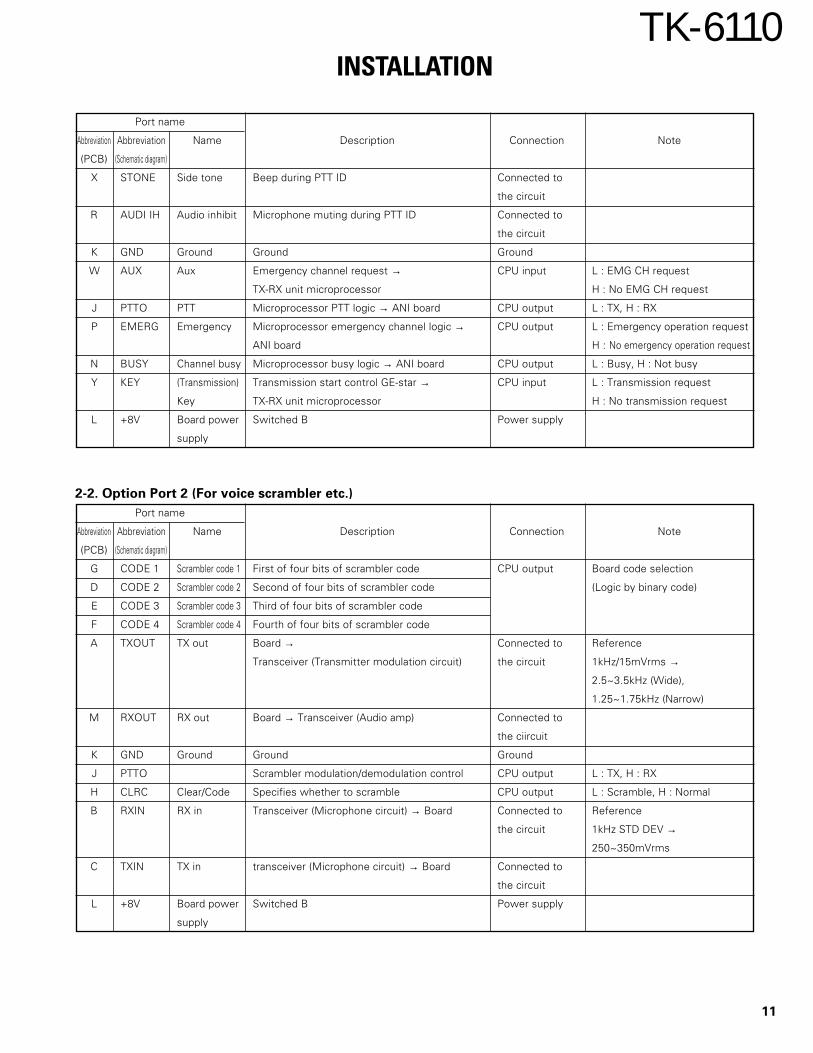
2-1. Option Port 1 (For ANI board etc.)
Port name
Abbreviation Abbreviation Name Description Connection Note
(PCB) (Schematic diagram)
B RX IN Data in Board data input. Connected to Reference
Transceiver (Receiver demodulaion circuit) → the circuit 1kHz STD DEV →
ANI board 250~350mVrms
T DATA Data out Board data output. Connected to Reference
Z TCONT T control Audio amplifier power control → CPU input L : Audio amp on
TX-RX unit microprocessor H : Audio amp off
Fig. 1
11
TK-6110
Port name
Abbreviation Abbreviation Name Description Connection Note
(PCB) (Schematic diagram)
X STONE Side tone Beep during PTT ID Connected to
the circuit
R AUDI IH Audio inhibit Microphone muting during PTT ID Connected to
the circuit
K GND Ground Ground Ground
W AUX Aux Emergency channel request → CPU input L : EMG CH request
TX-RX unit microprocessor H : No EMG CH request
J PTTO PTT Microprocessor PTT logic → ANI board CPU output L : TX, H : RX
P EMERG Emergency Microprocessor emergency channel logic → CPU output L : Emergency operation request
ANI board H : No emergency operation request
N BUSY Channel busy Microprocessor busy logic → ANI board CPU output L : Busy, H : Not busy
Y KEY (Transmission) Transmission start control GE-star → CPU input L : Transmission request
Key TX-RX unit microprocessor H : No transmission request
L +8V Board power Switched B Power supply
supply
2-2. Option Port 2 (For voice scrambler etc.)
Port name
Abbreviation Abbreviation Name Description Connection Note
(PCB) (Schematic diagram)
G CODE 1 Scrambler code 1 First of four bits of scrambler code CPU output Board code selection
D CODE 2 Scrambler code 2 Second of four bits of scrambler code (Logic by binary code)
E CODE 3 Scrambler code 3 Third of four bits of scrambler code
F CODE 4 Scrambler code 4 Fourth of four bits of scrambler code
A TXOUT TX out Board → Connected to Reference
Transceiver (Transmitter modulation circuit) the circuit 1kHz/15mVrms →
2.5~3.5kHz (Wide),
1.25~1.75kHz (Narrow)
M RXOUT RX out Board → Transceiver (Audio amp) Connected to
the ciircuit
K GND Ground Ground Ground
J PTTO Scrambler modulation/demodulation control CPU output L : TX, H : RX
H CLRC Clear/Code Specifies whether to scramble CPU output L : Scramble, H : Normal
B RXIN RX in Transceiver (Microphone circuit) → Board Connected to Reference
the circuit 1kHz STD DEV →
250~350mVrms
C TXIN TX in transceiver (Microphone circuit) → Board Connected to
the circuit
L +8V Board power Switched B Power supply
supply
INSTALLATION
12
TK-6110
3. Ignition Sense Cable (KCT-18)The KCT-18 is an optional cable to use the following func-
tions:
3-1. Ignition function
The ignition function allows you to turn the transceiver’spower on and off with the ignition key of your car. Whenyou are driving with the ignition key on, the horn alert func-tion is disabled.
3-2. Timed power off function
The timed power off function turns the transceiver’spower off the time specified with the programming soft-ware (KPG-59D) after the ignition key is turned off. Whenyou are driving with the ignition key on, the horn alert func-tion is disabled.
The ignition sense function and the timed power off func-tion can be used at the same time.
3-3. Modification
1. Remove the short plug from the accessory connector (15pins) on the back of the transceiver.
2. Insert the KCT-18 into pin 3 (IGN).
4. External Speaker (KES-4)1. The external speaker output from the accessory connec-
tor (15 pins) on the back of the transceiver is 10W/4ohms. Use the KES-4.
4-1. Connection for the KES-4 with the TK-6110
• When taking the AF output from the accessory
connector (15-pin) on the rear of the radio
The following tools are required for changing the connec-tor.Extracting tool
the following extracting tool is recommended :Molex Inc. Order No. : 11-03-0002
1. Remove the connector with jumper from the externalspeaker connector on the rear panel of the radio (Fig. 3-1).Note : Save the jumper, which is required when the radiois used without the external speaker.
INSTALLATION
Fig. 2
1313
15
KCT-18
Contact
Fig. 3-1 Fig. 3-2
Fig. 3-3
1
36
12
1315
Black/White leadBlack lead
2. Remove the terminals with the jumper from the connec-tor housing holes number 9 and 12 using the extractingtool.Removing the jumper lead (Fig. 3-2)1) Insert the extracting tool (11-03-0002) into the con-
nector while pushing the jumper lead in the directionof (a).
2) Push the extracting tool into collapse the barbs of thecrimp terminal.
3) Pull out the lead while continuing to push the extract-ing tool in the direction (b).
3. Reinsert the terminal with the black and white stripe leadinto hole number 6, and the terminal with the black leadinto hole number 12 (Fig. 3-3).
4. Attach the connector to the external speaker connectoron the radio.
5. Horn Alert FunctionThe HR pin of the accessory connector (15-pin) on the
rear of the transceiver is an open collector and the maxi-mum current is 100mA. The maximum available current canbe increased to 1A by installing a relay.
Program the Horn Alert Function, using KPG-59D.
Fig. 4
HR (Pin 10)
13
TK-6110CIRCUIT DESCRIPTION
Fig. 1 Frequency configuration
Fig. 2 Receiver section
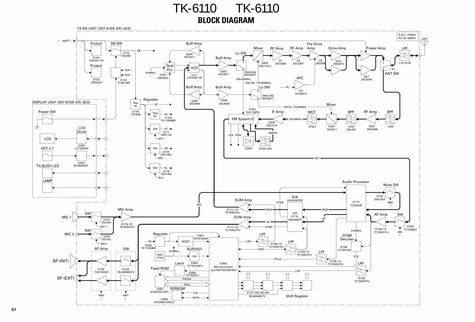
1. OverviewThe KENWOOD model TK-6110 is a VHF/FM transceiver
designed to operate in the frequency range of 29.7 to37MHz (K), 35.0 to 50.0MHz (K2), the unit consists of a re-ceiver, a transmitter, a phase-locked loop (PLL) frequencysynthesizer, power supply circuits, a control unit.
2. Circuit Configuration by FrequencyThe receiver is a double-conversion superheterodyne
with a first intermediate frequency (IF) of 128.55MHz and asecond IF of 455kHz. Incoming a signals from the antennaare mixed with the local signal from the PLL1 to produce thefirst IF of 128.55MHz.
This is then mixed with the 129.005MHz seconds localoscillator output to produce the 455kHz second IF. This isdetected to give the demodulated signal.
The transmit signal is modulated PLL2-VCO2 (129.005MHz) from the microphone. The transmit signal frequencyis down-conversion with PLL2 and PLL1. It is then amplifiedand sent to the antenna.
3. Receiver System
3-1. Front-End RF Amplifier
An incoming signal from the antenna is applied to a band-pass filter (L202) after going through a low-pass filter and anantenna switch (K1). The signal is then amplified by the RFamplifier (Q201) and again filtered by another band-pass fil-ter (L203, L206 and L207).
3-2. First Mixer
The signal from the band-pass filter is heterodyned withthe first local oscillator signal from the PLL frequency syn-thesizer circuit at the first mixer (IC201) to become a128.55MHz first intermediate frequency (IF) signal.
The first IF signal is fed through two monolithic crystalfilters (XF201) to further remove spurious signals.
3-3. IF Amplifier
The first IF signal is amplified by Q202 and Q205, andthen enters IC202 (FM processing IC). The signal is hetero-dyned again with a second local osci l lator signal(129.005MHz) with in IC202 to become a 455kHz second IFsignal. The second IF signal is fed through a 455kHz ce-ramic filter, CF201 and CF202 to further eliminate unwantedsignals before it is amplified and FM detected in IC202.
ANTTX/RX 29.7~37.0MHz : K35.0~50.0MHz : K2
29.7~37.0MHz : K35.0~50.0MHz : K2
LPF ANTSW
PAAMP
TXAMP
1st MIX
TX MIX
MCF128.55MHz
CF455kHz
FM IFSYSTEM
AFAMP
SP
129.005MHz
129.005MHz
PLL2VCO2
PLL1VCO1
MICAMP MIC
158.25~165.55MHz : K163.55~178.55MHz : K2
158.705~166.005MHz : K164.005~179.005MHz : K2
T/RSW
BPFQ201
RF AMP BPF BPF LPFIC201
1st MIX D502
MCF128.55MHz
Q205IF AMP
Q202IF AMP
IC202FM IF SYSTEM
CF201,202455kHz129.005MHz
XF201
Item Rating
Nominal center frequency 128.55MHzPass bandwidth ±7.5kHz or more at 3dBAttenuation bandwidth ±35kHz or less at 40dBRipple 1.0dB or lessInsertion loss 5dB or lessGuaranteed attenuation 70dB or more at fo±910kHzTerminating impedance 1000Ω
Table 1 Crystal filter (L71-0560-05)
(TX-RX unit XF201)
14
TK-6110CIRCUIT DESCRIPTION
Noiseamp
Noiseamp DET
Q206 D206
Outputexpander
IC604CPU
Mutecircuit
31SQL
7DETOUT
89
AF OUT
IC202
Fig. 4 squelch circuit
12HPF LPF HPF IDCPRE
EMPALC COMP
SW
LIMIT
D711IC713 15 16 18 19
Q708MM TONE
9 8
6
D/AIC710IC712
I4 O4
LSD
IC711 (1/2)
SUMAMP
IC714 (2/2)
AMPMIC1
SW
SW
SW VCO
L517
MIC2
MC1
MC2
(External input)
Fig. 5 Microphone circuit
3-4. Audio Amplifier Circuit
The recovered audio signal obtained from IC202 is ampli-fied by IC709, IC713, low-pass filtered by IC713 high-passfiltered by IC713 and band-eliminate filtered by IC713.
The audio signals then passed through a de-emphasizedby IC713. The processed audio signal passes through anaudio volume control and is amplified to a sufficient level todrive a loudspeaker by an audio power amplifier BTL(IC102).
4. Transmitter System
4-1. Microphone Amplifier
The signal from the microphone is high-pass filtered byIC713, passed through microphone mute and microphoneamplifier circuit (Q703 and IC714), limited and pre-empha-sized by IC713 and D711.
4-2. Modulator Circuit
The output of Audio-processor (IC703) is passed to the D/A converter (IC710) for maximum deviation adjustment andthe summing amplifier (IC711) before being applied to avaractor diode in the voltage controlled oscillator (VCO) lo-cated in the frequency synthesizer section.
4-3. Down-Mixer
At Q503, a modulated VCO2 signal is mixed with 2nd lo-cal oscillator signal, 129.005MHz. The difference of the twosignals is used for the transmission signal 29.7~37MHz (K),35.0~50.0MHz (K2). The output was filtered through a low-pass filter.
Fig. 3 Audio amplifier circuit
HPF
IC713
IC202FM IF SYSTEM
CF201,202455kHz
HPFLPF BEF
IC203
DE-EMP EXP
VOLSW
MUTE
129.005MHz
2 15 41
IC709 (2/2)AF AMP
IC711 (2/2)AF AMP
IC710
VOL
IC710AF
AMP
IC102
MUTE
IC105
ES2
AM1
3-5. Squelch Circuit
The output signal from IC202 enters FM IC again, thenpassed through a band-pass filter. The noise componentoutput from IC202 is amplified by Q206 and rectified byD205 to produce a DC 0 voltage corresponding to the noiselevel. The DC voltage is sent to the analog port of the CPU(IC604).
And IC202 outputs a DC voltage (RSSI) corresponding tothe input of the IF amplifier.
15
TK-6110CIRCUIT DESCRIPTION
4-4. Driver and Final Power amplifier Circuits
The transmit signal is generated by the TX mixer (Q503).The transmit signal obtained from the buffer amplifier Q1and Q2, is amplified by Q3 to approximately 30dBm. Thisamplified signal is amplified by Q4 and Q5 to approximately8W, and this signal is passed to the final stage.
The RF power amplifier consists of transistor (Q6 and Q7)and is capable of roducing up to 70W of RF power.
4-5. Transmit/Receive Switching Circuit
The final output signal is passed through a transmit/re-ceive switching circuit (K1) before it is passed to the an-tenna terminal.
4-6. Automatic Power Control, Circuit and Transmitter
The APC circuit consists of an RF level detector, an ex-citer control section and a temperature sensing circuit. TheRF level detector senses the forward and reflected power.The transmitter output power is kept constant by the excitercontrol circuit which monitors the forward power and regu-lates the supply voltage applied to the exciter section.
If the antenna load becomes abnormal, the reflectedpower increases, causing the exciter control circuit to re-duce the supply voltage to the exciter. In case of an abnor-mal temperature rise in the power amplifier section, thetemperature sensing circuit detects this condition and sendthe information to the APC circuit. These actions reduce thetransmitter output power to a safe operating level.
TXmixer
Q503
RFamp
Q1
RFamp
Q2
LPFPredriveamp
Q3
Driveamp
Q4
Driveamp
Q5
RF poweramp
Q6
TX/RXANT SW
K1
RF poweramp
Q7
ANT
Fig. 6 Drive and final amplifier
PDAT,PCLK,LE
TCXO
LPF
LPF
VCO2
VCO1
BUFF
BUFF
BUFF SW
BUFF
CPU
SW
16.8MHz
ULDual PLL
8TB/8R
8TB/8R
TXlocal 1
RXlocal 1
TXlocal 2
RXlocal 2
MOD/TONE
Fig. 7 PLL block diagram
5. PLL Frequency SynthesizerThe frequency synthesizer consists of the VCXO (X501),
VCO (L517), PLL IC (IC501) and buffer amplifiers.The VCXO generates 16.8MHz reference frequency. The
frequency stability is within ±5.0ppm (temperature range of–30 to +60°C). The output of the VCXO is applied to pin 8 ofthe PLL IC.
VCO (L517) has 2 internal VCOs. One for the 1st localoscillator (K : 158.25~166.005MHz, K2 : 163.55~179.005MHz) and another one for the 2nd local oscil lator(129.005MHz). Each output is connected to a dual PLL IC(IC501).
VCO1 oscillates at K : 158.705~166.005MHz, K2 :164.005~179.005MHz during transmission and it oscillatesat K : 158.25~165.55MHz, K2 : 163.55~178.55MHz duringreception.
VCO2 oscillates at 129.005MHz during both receptionand transmission. However, the oscillated signal is modu-lated during transmission. Each PLL circuit has LPFs andbuffer amplifiers.
The output of VCO1 goes through the buffer amplifier,then the output is switched either for the 1st local oscillatorcircuit of the receiver or TX mixer.
The output of VCO2 goes through the buffer amplifier,then the output is switched either for the 2nd local oscillatorcircuit of the receiver or TX mixer.
16
TK-6110CIRCUIT DESCRIPTION
6. Power Supply CircuitThe power (+B), which is suplied via a power connector,
is routed to the TX drive amplifier (Q4 and Q5), the TX finalamplifier (Q6 and Q7), and the audio power amplifier(IC102).
The power switch (Q110) converts the power (+B) to SB.The 8V REG (IC103) converts SB to 8C.
The two, 5V REGs (IC104 and IC602) converts 8C to 5Cand 5CM respectively. The 5CM is the power supplied tothe CPU. 8C is distributed between the TX circuit power (8Tand 8TB) and the RX circuit power (8R).
IC604CPU
INV
IC603
INV
IC603
VCXO
X501
X2
X1
to PLL
Fig. 10 CPU clock circuit
8V REG
IC103
5V REG
IC104
5V REG
IC602
SW
Q117
SW
Q118
SW
+BQ110
SW
Q119
Powercontrolcircuit
8TC
8TBC
8RC
+B
SB
5C
5CM
8C
8T
8TB
8R
Fig. 8 Power supply circuit
Addressdecode
IC604CPU
IC606
EEPROM
IC605
FlashROM
IC607
Fig. 9 Memory circuit
7. Control CircuitThe control unit circuit consists of microprocessor IC604
and flash memory IC607. It controls the TX-RX unit andtransfers data to and from the Display unit. The CPU (IC604)mainly performs the following :1) Switching between transmission and reception by PTT
signal input.2) Reading channel, frequency, and program data from the
memory circuit.3) Sending frequency program data to the PLL.4) Controlling squelch on/off from the squelch circuit.5) Controlling the audio mute circuit by decode data input.6) Transmitting encode data (QT, DQT).7) Sending serial data to output expander (IC704, IC701,
IC702 and IC703) to control various function in the unit.
7-1. Memory Circuit
IC607 has a flash memory with a capacity of 2M bits thatcontains the transceiver control program for the CPU anddata such as transceiver channels and operating features.
This program can be easily written from an external de-vices. Data, such as DTMF memories and operating status,are programmed into the EEPROM (IC605).
7-2. CPU Clock
The CPU clock is generated by VCXO (16.8MHz) and it isfed through an inverter, IC603. This clock was divided into ahalf cycle (1/2 frequency) at the internal CPU. The CPU fur-ther divides this clock to utilize it as the various clocks.
7-3. Shift Register
IC704, IC701, IC702 and IC703 is an interface IC for out-put port expansion. It is used to expand the CPU (IC604)output ports.
7-4. D/A Converter
IC715 and IC710 is used as a conventional semi-fixed-resistor converter. It sets the following :1) RX filter tuning2) Transmission power tuning3) Modulation level tuning4) Audio power tuning
7-5. Key Input (Display unit)
K1 or K2 becomes High when any key is pressed (or en-able signal on the optional circuit).
When K1 or K2 becomes High, to trigger the interrupt toIC604 in order to start the key scan.
When the key scan starts, the output terminals IC901(Q1~Q5) become Low. Only the key sensing circuit remainsHigh. When a key is pressed, the signal is routed throughK1 or K2 to the microprocessor. Then, the microprocessordetermines which key is pressed using this signals.
17
TK-6110
8. Signalling Circuit
8-1. Encode
The CPU (IC604) transmits the encode data selected bythe program.
• Low-speed data (QT, DQT)
Low-speed data is output from pin 34 of the CPU. Thesignal passes through a low-pass filter consisting of IC706(2/2), and goes to the summing amplifier (IC711 1/2). Thesignal is mixed with the audio signal and goes to the VCO(L517).
• High-speed data (DTMF)
High-speed data is output from pin 35 of the CPU. Thesignal passes through a low-pass filter consisting of IC706(1/2), and provides a TX DTMF tone and a RX DTMF toneincluding a beep tone. The TX DTMF tone is passed to theD/A convertor (IC710) for DTMF deviation adjustment, andthen applied to the audio processor (IC713).
The signal is mixed with the audio signal and goes to theVCO. The RX DTMF tone is passed the D/A convertor(IC710) for audio control summing amplifier (IC711 2/2), au-dio power amplifier and then to the speaker.
IC708DTMF
DECODE
IC709(2/2)AMP
IC705LPF
IC713AF
IC709 (1/2)LPF
from IC202FM IC
2TON
LSD IN
IC604CPU
STDDCKSD
Fig. 13 Decode
CIRCUIT DESCRIPTION
IC901
D913D912 D914 D915
CHUP MON B SCN
CHDN A C
Q1 Q3 Q4 Q5
IC604CPU
CLK,DAT,LCDCS
K1
K2
Fig. 11 Key input
IC604CPU
LPF SUM
LPF SUM
SUM
VCO2
HSDO
LSDO
TX AUDIO
RX AUDIO
to AF AMP
MOD
IC710DAC(ADJ)
Fig. 12 Encode
8-2. Decode
• Low-speed data (QT, DQT)
The demodulated signal from the FM IC (IC202) is ampli-fied by IC709 (2/2) and passes through a low-pass filter(IC705) to remove audio components. The signal is input topin 28 of the CPU.
The CPU digitizes this signal, performs processing suchas DC restoration, and decodes the signal.
• High-speed data (DTMF)
The DTMF input signal from the FM IC (IC202) is ampli-fied by IC709 (2/2) and goes to IC708, the DTMF decoder.The decoded information is then processed by the CPU.During transmission and standby, the PD terminal is High.When the line is busy, the PD terminal becomes Low, thepower down mode is canceled and decoding is carried out.
• High-speed data (2-tone)
The demodulated signal from the FM IC (IC202) is ampli-fied by IC709 (2/2) and passes through an audio processor(IC713) and low-pass filter (IC709 1/2) to remove a low-speed data.
The CPU digitizes this signal, performs processing suchas DC restoration, and decodes the signal.
18
TK-6110
• Terminal function
Pin No. Pin name I/O Action
1 FCLR O Modem FCLR
2 POF O Power off
3 LD O D/A converter CS (M62364FP)
4 MSKE O Modem MSK enable
5 MDAT O Modem Data/TX Data
6 MD1 I Model select 1
7 MD2 I Model select 2
8 NC
9 VDD – +5V
10 X2 – Ext. clock
11 X1 – Ext. clock
12 VSS – GND
13 XT2 – Open
14 XT1 – GND
15 RESET – CPU reset
16 SENSB I GE-STAR SENS B
17 TRD I Modem TRD
18 RTM I Modem RTM
19 STD I DTMF decoder STD
20 NC
21 PSW I Power SW detect
22 HK1 I MIC hook 1 (RXD1)
23 AVDD – +5V
24 AVREF0 – +5V
25 AUXGE I GE-STAR AUX
26 VOL I AF volume
27 TMP I Temperature
28 LSD IN I QT/DQT input
29 IGN I Ignition sense L : ON, H : OFF
30 UL I PLL unlock detect
31 SQL I SQL level
32 RSSI I RSSI level
33 AVSS – GND
34 LSDO O QT/DQT output
35 HSDO O DTMF/BEEP output
36 AVREF1 – +5V
37,38 NC
39 PDAT O PLL data
40 RXD1 I Serial interface RXD
41 PTT1/TXD1 I/O MIC PTT/ Serial interface TXD
42 MSTB O Modem STB
43 DCK O DTMF decoder clock
44 SD I DTMF SD
45 LCDCS O LCD CS
SEMICONDUCTOR DATA
Pin No. Pin name I/O Action
46 STB1 O Shift register 1 STB
47 STB2 O Shift register 2 STB
48~71 Cannot use. Flash ROM access port.
72 VSS – GND
73~74 Cannot use. Flash ROM access port.
75 Cannot use. Flash ROM (4Mbit)
access port.
76 Cannot use open
77~78 Cannot use. Flash ROM access port.
79 KEY I GE-STAR KEY
80 NC Cannot use open
81 VDD – +5V
82 SCL O EEPROM clock
83 SDA I/O EEPROM data
84 CLK O Common clock
85 DATA O Common data
86 CM I DTMF MIC key pad data
87 K1 I Key scan counter return 1
88 K2 I Key scan counter return 2
89 PCLK O PLL clock
90 KES O Key scan counter enable
91 2TON I 2-Tone
92 SOE O Shift register output enable
93 LE O PLL latch enable
94 TEST - GND
95 TCNT I GE-STAR TCONT
96 PTT2 I EXT PTT
97 HK2 I EXT hook
98 FSW I Foot SW
99 LD2 O D/A converter CS (M62354GP)
100 RDT I Modem RDT
Shift Register Output
• Shift Register 1 (TX-RX unit IC704)
Pin No. Port Name Action
4 Q1 8RBC 8RB control SW L : OFF, H : ON
5 Q2 8RC 8R control SW L : OFF, H : ON
6 Q3 8TBC 8TB control SW L : OFF, H : ON
7 Q4 8TC 8R control SW L : OFF, H : ON
14 Q5 – Reserved
13 Q6 – Not used
12 Q7 – Reserved
11 Q8 NBS NB control SW L : OFF, H : ON
Microprocessor : 784214GC0618EU (TX-RX Unit IC604)
19
TK-6110
• Shift Register 2 (TX-RX unit IC701)
Pin No. Port Name Action
4 Q1 AM1 Audio mute 1 L : Mute, H : Unmute
5 Q2 REG1 Modem REG1
6 Q3 REG2 Modem REG2
7 Q4 PD DTMF PD
14 Q5 AUX ACC AUX
13 Q6 – Not used
12 Q7 AM2 Audio mute 2 L : Unmute, H : Mute
11 Q8 – Not used
• Shift Register 3 (TX-RX unit IC702)
Pin No. Port Name Action
4 Q1 BLC LCD, KEY back light SW L : OFF, H : ON
5 Q2 RXLED Busy LED SW L : ON, H : OFF
6 Q3 TXLED TX LED SW L : ON, H : OFF
7 Q4 MM Modem, GE-STAR L : Mute, H : Unmute
14 Q5 HRC Horn alert control SW L : OFF, H : ON
13 Q6 MC1 Internal MIC SW L : Mute, H : Unmute
12 Q7 MC2 External MIC SW L : Mute, H : Unmute
11 Q8 – Not used
• Shift Register 4 (TX-RX unit IC703)
Pin No. Port Name Action
4 Q1 PTTO GE-STAR, Scrambler PTT
5 Q2 CLRC Scrambler CLR code L : ON, H : OFF
6 Q3 CHBS GE-STAR Channel Busy
7 Q4 EMRG GE-STAR EMRG
14 Q5 COD1 Scrambler code set
13 Q6 COD2 Scrambler code set
12 Q7 COD3 Scrambler code set
11 Q8 COD4 Scrambler code set
RF Final Amplifier : 2SC2540 (TX-RX Unit Q6,Q7)
• Absolute maximum ratings
Symbol Parameter Condition Rating
VCBO Collector to base voltage 35V
VEBO Emitter to base voltage 4V
VCEO Collector to emitter voltage RBE=∞ 17V
IC Collector current 10A
PC Collector dissipation 75W
Tj Junction temperature +175°C
Tstg Storage temperature –55~+175°C
Audio Power Amplifier : TDA1519A
(TX-RX Unit IC102)
• Block Diagram
• Terminal function
Pin No. Symbol Description
1 NINV Non-inverting input
2 GND1 Ground (signal)
3 RR Supply voltage ripple rejection
4 OUT1 Output 1
5 GND2 Ground (substrate)
6 OUT2 Output 2
7 Vp Positive supply voltage
8 M/SS Mute/stand-by switch
9 INV Inverting input
SEMICONDUCTOR DATA
1
60kΩ
mute switch
Cm
VA
183Ω
18.1kΩpowerstage
4
8
Vp
stand-byswitch
VA
+–
stand-byreferencevoltage
muteswitch
++
+
–
mutereferencevoltage
15kΩ
x13
18.1kΩ
183Ω
60kΩ
VA
mute switch
Cm
powerstage
6
inputreference
voltage signalground Vp
powerground(substrate)
572
9
20
TK-6110DESCRIPTION OF COMPONENTS
TX-RX Unit (X57-6100-XX) (A/3)
-10 : K -11 : K2
Ref. No. Use/Function Operation/Condition
IC2 APC comparator APC control
IC101 D Flip-Flop Power supply control
IC102 Audio power amplifier 10W/4Ω, BTL method
IC103 Voltage regulator Input : SB, Output : 8V
IC104 Voltage regulator Input : 8V, Output : 5V
IC105 Analog switch Audio mute switch
IC201 Active DBM RX 1st mixer
IC202 FM IF system 2nd mixer, Detector, IF amp,
Noise amp
IC203 Analog switch Audio mute switch
IC401 AGC amplifier
IC501 Dual-PLL
IC601 Voltage detector Microprocessor reset
IC602 Voltage regulator Input : 8V, Output : 5V
IC603 Buffer amplifier Microprocessor clock
IC604 Microprocessor
IC605 EEPROM
IC606 NOR gate Address decode latch
IC607 Flash ROM
IC701~704 Shift register Output expander
IC705 Active low pass filter LPF for LSD input
IC706 Active low pass filter LPF for HSD, LSD output
IC707 Buffer amplifier 1/2V Ref, Ext. DET amplifier
IC708 DTMF decoder
IC709 Buffer amplifier/ DET amplifier/LPF for 2-tone
Q903 LCD back light switch BLC “L” : Off, “H” : On
Q904 LCD back light switch BLC “L” : Off, “H” : On
Q905 KEY back light switch BLC “L” : Off, “H” : On
D901 LED for TX,
RX LED light
D902~907 LED for LCD back light
D908~911 LED for KEY back light
D912~915 Protection of reverse current
D916 Speed up
TK-6110PARTS LIST
22
*New Parts. indicates safety critical components.Parts without Parts No. are not supplied.Les articles non mentionnes dans le Parts No. ne sont pas fournis.Teile ohne Parts No. werden nicht geliefert.
L : Scandinavia K : USA P : CanadaY : PX (Far East, Hawaii) T : England E : EuropeY : AAFES (Europe) X : Australia M: Other Areas
TK-6110
TX-RX UNIT (X57-6100-XX)
New Desti-parts nationRef. No. Address Parts No. Description New Desti-
parts nationRef. No. Address Parts No. Description
A 1B N33-2606-45 OVAL HEAD MACHINE SCREW (CASE)B 1A N67-3008-46 PAN HEAD SEMS SCREW W (FINAL AMP)C 2B N87-2606-45 BRAZIER HEAD TAPTITE SCREW (ANT,15P)D 1A,1B,2B N87-2606-46 BRAZIER HEAD TAPTITE SCREW (PCB)62 2D N99-0395-05 SCREW SET ACSY
D901 B30-2151-05 LED (RED/GREEN)D902-907 B30-2140-05 LED (Y/8)D908-911 B30-2050-05 LED
C1 CK73GB1H103K CHIP C 0.010UF KC3 CC73GCH1H270J CHIP C 27PF J K2C3 CC73GCH1H470J CHIP C 47PF J KC4 CK73GB1H103K CHIP C 0.010UF KC5 CC73GCH1H101J CHIP C 100PF J K2
C6 CK73GB1H103K CHIP C 0.010UF KC7 CK73GB1H102K CHIP C 1000PF KC8 CK73GB1H103K CHIP C 0.010UF KC9 CC73GCH1H101J CHIP C 100PF J KC9 CC73GCH1H680J CHIP C 68PF J K2
C11 CC73GCH1H101J CHIP C 100PF J KC11 CK73GB1H103K CHIP C 0.010UF K K2C13 CK73GB1H472K CHIP C 4700PF KC14 CK73GB1H103K CHIP C 0.010UF KC15,16 CK73GB1H472K CHIP C 4700PF K
C17-19 CK73GB1H103K CHIP C 0.010UF KC20 CC73GCH1H470J CHIP C 47PF J K2C20 CC73GCH1H560J CHIP C 56PF J KC21,22 CC73GCH1H101J CHIP C 100PF J K2C21,22 CC73GCH1H121J CHIP C 120PF J K
C23 CC73GCH1H470J CHIP C 47PF J K2C23 CC73GCH1H560J CHIP C 56PF J KC24 CC73GCH1H390J CHIP C 39PF J K2C24 CC73GCH1H680J CHIP C 68PF J KC25 CK73GB1H103K CHIP C 0.010UF K
C28,29 CK73GB1H103K CHIP C 0.010UF KC30 * C93-0596-05 CHIP C 270PF K K2C30 C93-0600-05 CHIP C 560PF K KC31 CE04EW1E470M ELECTRO 47UF 25WVC32 CK73GB1H103K CHIP C 0.010UF K
C33 CK73GB1H472K CHIP C 4700PF KC34 CK73GB1H103K CHIP C 0.010UF KC35 C92-0633-05 CHIP-TAN 22UF 10WVC36 CK73GB1H103K CHIP C 0.010UF KC39,40 * C93-0684-05 CERAMIC 6800PF K
C45 * C90-4085-05 ELECTRO 47UF 20WVC46 CK73FB1E104K CHIP C 0.10UF KC47 CK73GB1H472K CHIP C 4700PF KC48 CC73GCH1H101J CHIP C 100PF J
TX-RX UNIT (X57-6100-XX) -10 : K -11 : K2
TK-6110PARTS LIST
23
Ref. No. Address Parts No. Description Ref. No. Address Parts No. DescriptionNew Desti-parts nation
New Desti-parts nation
C49 CK73FB1E104K CHIP C 0.10UF KC50 CK73GB1H103K CHIP C 0.010UF KC51 CK73FB1E103K CHIP C 0.010UF KC52 CK73GB1H103K CHIP C 0.010UF KC54 CC73GCH1H020B CHIP C 2.0PF B
C55 CC73GCH1H820J CHIP C 82PF JC56 CK73GB1H103K CHIP C 0.010UF KC58 CK73FB1E104K CHIP C 0.10UF KC59-61 CK73GB1H103K CHIP C 0.010UF KC62 CC73GCH1H680J CHIP C 68PF J
C63 CK73GB1H103K CHIP C 0.010UF KC64 CC73GCH1H020B CHIP C 2.0PF BC65,66 CC73GCH1H220J CHIP C 22PF J K2C65,66 CC73GCH1H390J CHIP C 39PF J KC68,69 CK73GB1C473K CHIP C 0.047UF K
C70 CM73F2H470J CHIP C 47PF J K2C70 CM73F2H820J CHIP C 82PF J KC71 CM73F2H080D CHIP C 8.0PF D KC71 CM73F2H090D CHIP C 9.0PF D K2C72 CM73F2H101J CHIP C 100PF J K2
C72 CM73F2H181J CHIP C 180PF J KC73 CK73GB1H103K CHIP C 0.010UF KC75 CM73F2H180J CHIP C 18PF J KC75 CM73F2H220J CHIP C 22PF J K2C76 CM73F2H470J CHIP C 47PF J K2
C76,77 CM73F2H820J CHIP C 82PF J KC77 CM73F2H390J CHIP C 39PF J K2C78 CM73F2H510J CHIP C 51PF JC79 CM73F2H390J CHIP C 39PF J K2C79 CM73F2H820J CHIP C 82PF J K
C80 CK73GB1H103K CHIP C 0.010UF KC81 CC73GCH1H470J CHIP C 47PF J K2C81 CC73GCH1H560J CHIP C 56PF J KC82 CC73GCH1H101J CHIP C 100PF J K2C82 CC73GCH1H121J CHIP C 120PF J K
C83 CC73GCH1H470J CHIP C 47PF J K2C83 CC73GCH1H560J CHIP C 56PF J KC84,85 CC73GCH1H220J CHIP C 22PF J K2C84,85 CC73GCH1H390J CHIP C 39PF J KC86 CC73GCH1H270J CHIP C 27PF J K2
C86 CC73GCH1H560J CHIP C 56PF J KC87,88 CC73GCH1H220J CHIP C 22PF J K2C87,88 CC73GCH1H390J CHIP C 39PF J KC89 CC73GCH1H470J CHIP C 47PF J K2C89 CC73GCH1H560J CHIP C 56PF J K
C90 CC73GCH1H101J CHIP C 100PF J K2C90 CC73GCH1H121J CHIP C 120PF J KC91 CC73GCH1H470J CHIP C 47PF J K2C91 CC73GCH1H560J CHIP C 56PF J KC92-96 CK73GB1H103K CHIP C 0.010UF K
C99 C93-0601-05 CHIP C 680PF KC100 CM73F2H561J CHIP C 560PF JC101 CE04EW1E471M ELECTRO 470UF 25WVC102 CK73GB1H472K CHIP C 4700PF KC103 C92-0777-05 ELECTRO 1000UF 25WV
C104 CE04NW1E4R7M ELECTRO 4.7UF 25WVC105,106 CK73FB1E104K CHIP C 0.10UF KC107 CK73FB1E224K CHIP C 0.22UF KC108 CE04EW1E470M ELECTRO 47UF 25WVC109,110 CK73FB1E104K CHIP C 0.10UF K
C111 CE04EW1E101M ELECTRO 100UF 25WVC112 CE04EW1E470M ELECTRO 47UF 25WVC113 C92-0560-05 CHIP-TAN 10UF 6.3WVC114,115 CK73FB1E224K CHIP C 0.22UF KC116,117 CK73GB1H102K CHIP C 1000PF K
C118,119 CK73FB1E104K CHIP C 0.10UF KC120 CE04EW1E470M ELECTRO 47UF 25WVC121 CK73FF1C105Z CHIP C 1.0UF ZC122 CK73GB1H471K CHIP C 470PF KC123-126 CK73GB1H103K CHIP C 0.010UF K
C128 CK73FF1C105Z CHIP C 1.0UF ZC129 CK73GB1H471K CHIP C 470PF KC130 C92-0589-05 CHIP-TAN 47UF 6.3WVC131 CK73GB1H102K CHIP C 1000PF KC132,133 CK73GB1H103K CHIP C 0.010UF K
C134 CK73FB1E104K CHIP C 0.10UF KC135,136 C92-0560-05 CHIP-TAN 10UF 6.3WVC137,138 CK73FB1E224K CHIP C 0.22UF KC139 CK73GB1C104K CHIP C 0.10UF KC140 CK73FB1E224K CHIP C 0.22UF K
C141 CK73GB1C104K CHIP C 0.10UF KC142 CK73GB1H471K CHIP C 470PF KC197,198 CM73F2H121J CHIP C 120PF J KC196,199 CM73F2H181J CHIP C 180PF J K2C196,199 CM73F2H330J CHIP C 33PF J K
C197,198 CM73F2H331J CHIP C 330PF J K2C203 CC73GCH1H101J CHIP C 100PF JC204 CC73GCH1H050C CHIP C 5.0PF C K2C205 CC73GCH1H390J CHIP C 39PF J KC205 CC73GCH1H470J CHIP C 47PF J K2
C206 CK73GB1H103K CHIP C 0.010UF KC208 CK73GB1H102K CHIP C 1000PF KC209 C92-0628-05 CHIP-TAN 10UF 10WVC210-212 CK73GB1H103K CHIP C 0.010UF KC213 CC73GCH1H050C CHIP C 5.0PF C K2
C214 CK73GB1H103K CHIP C 0.010UF KC215 CC73GCH1H390J CHIP C 39PF J KC215 CC73GCH1H470J CHIP C 47PF J K2C217-219 CK73GB1H103K CHIP C 0.010UF KC221 CC73GCH1H050C CHIP C 5.0PF C K2
C222 CC73GCH1H101J CHIP C 100PF JC225 CC73GCH1H270J CHIP C 27PF JC226 CK73GB1H102K CHIP C 1000PF KC227 CC73GCH1H100D CHIP C 10PF DC228 CC73GCH1H180J CHIP C 18PF J
C229 CC73GCH1H040C CHIP C 4.0PF CC230 CC73GCH1H680J CHIP C 68PF JC231,232 CK73GB1H103K CHIP C 0.010UF KC233 CK73GB1H471K CHIP C 470PF KC235 CK73GB1H471K CHIP C 470PF K
C236-238 CK73GB1H102K CHIP C 1000PF KC239 CC73GCH1H030C CHIP C 3.0PF CC240 CC73GCH1H180J CHIP C 18PF JC241 CK73GB1H102K CHIP C 1000PF KC242 CK73GB1C473K CHIP C 0.047UF K
C243 CK73GB1H102K CHIP C 1000PF KC245 CC73GCH1H1R5B CHIP C 1.5PF BC246 CK73GB1H102K CHIP C 1000PF KC247,248 CK73GB1H103K CHIP C 0.010UF KC249 CC73GCH1H010B CHIP C 1.0PF B
TX-RX UNIT (X57-6100-XX)
TK-6110PARTS LIST
24
C250 CC73GCH1H020B CHIP C 2.0PF BC251 CC73GCH1H010B CHIP C 1.0PF BC252 CK73GB1H102K CHIP C 1000PF KC253 CK73GB1H103K CHIP C 0.010UF KC255 CK73GB1H102K CHIP C 1000PF K
C256 CK73GB1C104K CHIP C 0.10UF KC257-259 CK73GB1H102K CHIP C 1000PF KC260 CC73GCH1H030C CHIP C 3.0PF CC262 CK73GB1C104K CHIP C 0.10UF KC263 CK73GB1H102K CHIP C 1000PF K
C264 C92-0004-05 CHIP-TAN 1.0UF 16WVC266 CC73GCH1H270J CHIP C 27PF JC267,268 CK73GB1C104K CHIP C 0.10UF KC269 CK73GB1H102K CHIP C 1000PF KC270 CC73GCH1H221J CHIP C 220PF J
C271 CK73GB1H103K CHIP C 0.010UF KC272 CC73GCH1H221J CHIP C 220PF JC273 CK73GB1E223K CHIP C 0.022UF KC274 CK73GB1H472K CHIP C 4700PF KC275,276 CK73GB1H102K CHIP C 1000PF K
C277 CK73FB1H223K CHIP C 0.022UF KC278 C92-0560-05 CHIP-TAN 10UF 6.3WVC279 CK73FB1C334K CHIP C 0.33UF KC280 CK73GB1H103K CHIP C 0.010UF KC281 C92-0560-05 CHIP-TAN 10UF 6.3WV
C282 CK73GB1H103K CHIP C 0.010UF KC284 CC73GCH1H390J CHIP C 39PF J KC284 CC73GCH1H470J CHIP C 47PF J K2C285,286 CC73GCH1H150J CHIP C 15PF JC287 CC73GCH1H020B CHIP C 2.0PF B
C288 CC73GCH1H150J CHIP C 15PF JC290 CC73GCH1H020B CHIP C 2.0PF BC291 CC73GCH1H101J CHIP C 100PF JC293 CC73GCH1H020B CHIP C 2.0PF BC294 CC73GCH1H150J CHIP C 15PF J
C296 CC73GCH1H020B CHIP C 2.0PF BC297 CC73GCH1H180J CHIP C 18PF JC299 CC73GCH1H020B CHIP C 2.0PF BC300 CC73GCH1H270J CHIP C 27PF JC301 CC73GCH1H040C CHIP C 4.0PF C
C302 CC73GCH1H020B CHIP C 2.0PF BC303 CC73GCH1H220J CHIP C 22PF JC304 CC73GCH1H040C CHIP C 4.0PF CC305 CC73GCH1H020B CHIP C 2.0PF BC306 CC73GCH1H330J CHIP C 33PF J
C307,308 CK73GB1H102K CHIP C 1000PF KC309 CC73GCH1H010B CHIP C 1.0PF BC401 C92-0543-05 CHIP-TAN 3.3UF 10WVC402 CC73GCH1H680J CHIP C 68PF JC403 CK73GB1H103K CHIP C 0.010UF K
C404 CK73GB1C104K CHIP C 0.10UF KC405 C92-0543-05 CHIP-TAN 3.3UF 10WVC406 CK73GB1H103K CHIP C 0.010UF KC407 CC73GCH1H220J CHIP C 22PF JC408 CC73GCH1H470J CHIP C 47PF J
C409,410 CK73GB1H103K CHIP C 0.010UF KC411 CK73GB1H102K CHIP C 1000PF KC412,413 CK73GB1C104K CHIP C 0.10UF KC414 CK73GB1H103K CHIP C 0.010UF KC415 CC73GCH1H220J CHIP C 22PF J
C416 CK73GB1H102K CHIP C 1000PF KC417 CC73GCH1H221J CHIP C 220PF JC418 CC73GCH1H680J CHIP C 68PF JC419-421 CK73GB1H103K CHIP C 0.010UF KC422 CC73GCH1H221J CHIP C 220PF J
C423 C92-0543-05 CHIP-TAN 3.3UF 10WVC424 CK73GB1H102K CHIP C 1000PF KC425 CK73GB1H103K CHIP C 0.010UF KC501 C92-0560-05 CHIP-TAN 10UF 6.3WVC502 CC73GCH1H100D CHIP C 10PF D
C503 CK73GB1H103K CHIP C 0.010UF KC504,505 CK73GB1H102K CHIP C 1000PF KC507 C92-0560-05 CHIP-TAN 10UF 6.3WVC510 C92-0589-05 CHIP-TAN 47UF 6.3WVC511,512 CK73GB1H103K CHIP C 0.010UF K
C513 CC73GCH1H100D CHIP C 10PF DC514 CK73GB1H102K CHIP C 1000PF KC516 CC73GCH1H100D CHIP C 10PF DC517,518 CK73GB1H102K CHIP C 1000PF KC519 CK73GB1H103K CHIP C 0.010UF K
C521 CK73GB1H103K CHIP C 0.010UF KC522 C92-0507-05 CHIP-TAN 4.7UF 6.3WVC523,524 CK73GB1H102K CHIP C 1000PF KC525 CK73GB1H222K CHIP C 2200PF KC526 CC73GCH1H101J CHIP C 100PF J
C527 C92-0507-05 CHIP-TAN 4.7UF 6.3WVC528 CC73GCH1H120J CHIP C 12PF JC529 CC73GCH1H470J CHIP C 47PF JC530 CK73GB1H102K CHIP C 1000PF KC531-533 CC73GCH1H101J CHIP C 100PF J
C534,535 CK73GB1H102K CHIP C 1000PF KC536 CC73GCH1H101J CHIP C 100PF JC537 CK73GB1H102K CHIP C 1000PF KC538 CC73GCH1H180J CHIP C 18PF JC539 CK73GB1H103K CHIP C 0.010UF K
C540 CK73GB1H102K CHIP C 1000PF KC541 CC73GCH1H101J CHIP C 100PF JC542 C92-0001-05 CHIP C 0.1UF 35WVC543 C92-0560-05 CHIP-TAN 10UF 6.3WVC544 C92-0004-05 CHIP-TAN 1.0UF 16WV
C545,546 C92-0589-05 CHIP-TAN 47UF 6.3WVC547 CK73GB1C473K CHIP C 0.047UF KC548 CK73GB1H102K CHIP C 1000PF K K2C548,549 CK73GB1H102K CHIP C 1000PF K KC549 CC73GCH1H101J CHIP C 100PF J K2
C550 CC73GCH1H070D CHIP C 7.0PF D K2C550 CC73GCH1H100D CHIP C 10PF D KC551 C92-0004-05 CHIP-TAN 1.0UF 16WVC552 CK73GB1H103K CHIP C 0.010UF KC553 C92-0560-05 CHIP-TAN 10UF 6.3WV
C554 CK73GB1H102K CHIP C 1000PF KC555 CC73GCH1H060D CHIP C 6.0PF DC557 CK73GB1H102K CHIP C 1000PF KC559 CC73GCH1H220J CHIP C 22PF JC560,561 CK73GB1H102K CHIP C 1000PF K
C564 CC73GCH1H180J CHIP C 18PF JC565 CC73GCH1H470J CHIP C 47PF JC568 CK73GB1H102K CHIP C 1000PF KC569 CC73GCH1H390J CHIP C 39PF JC570 CC73GCH1H220J CHIP C 22PF J
TX-RX UNIT (X57-6100-XX)
Ref. No. Address Parts No. Description Ref. No. Address Parts No. DescriptionNew Desti-parts nation
New Desti-parts nation
TK-6110PARTS LIST
25
Ref. No. Address Parts No. Description Ref. No. Address Parts No. DescriptionNew Desti-parts nation
New Desti-parts nation
C571 CK73GB1H102K CHIP C 1000PF KC573 CC73GCH1H090D CHIP C 9.0PF DC574 CC73GCH1H180J CHIP C 18PF JC575,576 CK73GB1H102K CHIP C 1000PF KC577 CC73GCH1H270J CHIP C 27PF J
C578 CC73GCH1H150J CHIP C 15PF JC579 CC73GCH1H070D CHIP C 7.0PF DC580 CC73GCH1H060D CHIP C 6.0PF D KC581 CC73GCH1H040C CHIP C 4.0PF CC582 CK73GB1H102K CHIP C 1000PF K
C583 CC73GCH1H270J CHIP C 27PF JC584 CC73GCH1H150J CHIP C 15PF JC585 CK73GB1H102K CHIP C 1000PF KC586 CC73GCH1H100D CHIP C 10PF DC587 CC73GCH1H090D CHIP C 9.0PF D
C588-594 CK73GB1H102K CHIP C 1000PF KC595 CC73GCH1H220J CHIP C 22PF JC596 CK73GB1H103K CHIP C 0.010UF KC598 CK73GB1H103K CHIP C 0.010UF KC599 CC73GCH1H470J CHIP C 47PF J
C601 CK73GB1H102K CHIP C 1000PF KC602 CK73FF1C105Z CHIP C 1.0UF ZC603 CK73GB1H471K CHIP C 470PF KC604 CK73GB1H103K CHIP C 0.010UF KC605 CK73GB1H222K CHIP C 2200PF K
C606 CK73FF1C105Z CHIP C 1.0UF ZC607 CK73GB1H222K CHIP C 2200PF KC608 CK73GB1H471K CHIP C 470PF KC609 C92-0589-05 CHIP-TAN 47UF 6.3WVC610 CK73GB1H102K CHIP C 1000PF K
C611-639 CC73HCH1H101J CHIP C 100PF JC640 CK73GB1H102K CHIP C 1000PF KC641 C92-0560-05 CHIP-TAN 10UF 6.3WVC642 CK73GB1H102K CHIP C 1000PF KC643 CK73GB1C104K CHIP C 0.10UF K
C703 CK73GB1C104K CHIP C 0.10UF KC704 C92-0560-05 CHIP-TAN 10UF 6.3WVC707 CC73GCH1H151J CHIP C 150PF JC711 CK73GB1C104K CHIP C 0.10UF KC715 CK73GB1C104K CHIP C 0.10UF K
C716 CK73GB1H471K CHIP C 470PF KC720 CK73GB1H103K CHIP C 0.010UF KC723 CK73GB1H103K CHIP C 0.010UF KC725,726 CC73GCH1H101J CHIP C 100PF JC728 CK73GB1H471K CHIP C 470PF K
C730,731 CC73GCH1H101J CHIP C 100PF JC733 CK73GB1C104K CHIP C 0.10UF KC734,735 CC73GCH1H101J CHIP C 100PF JC737 CK73GB1C104K CHIP C 0.10UF KC738,739 CC73GCH1H101J CHIP C 100PF J
C741,742 CC73GCH1H101J CHIP C 100PF JC744,745 CC73GCH1H101J CHIP C 100PF JC747,748 CC73GCH1H101J CHIP C 100PF JC750,751 CC73GCH1H101J CHIP C 100PF JC753,754 CC73GCH1H101J CHIP C 100PF J
C756 CC73GCH1H101J CHIP C 100PF JC757 CK73GB1H102K CHIP C 1000PF KC759 CC73GCH1H101J CHIP C 100PF JC760 C92-0560-05 CHIP-TAN 10UF 6.3WVC764-767 CK73GB1H102K CHIP C 1000PF K
C768 CK73GB1C333K CHIP C 0.033UF KC770 CC73GCH1H121J CHIP C 120PF JC771 CK73GB1H103K CHIP C 0.010UF KC772 CK73GB1C273K CHIP C 0.027UF KC773 CK73GB1H103K CHIP C 0.010UF K
C774 CK73GB1H222K CHIP C 2200PF KC775 CC73GCH1H271J CHIP C 270PF JC776 CK73GB1H103K CHIP C 0.010UF KC777 CK73GB1H472K CHIP C 4700PF KC778 CK73GB1E123K CHIP C 0.012UF K
C779 CK73GB1C683K CHIP C 0.068UF KC780 CK73GB1H103K CHIP C 0.010UF KC781 CC73GCH1H101J CHIP C 100PF JC782 C92-0003-05 CHIP-TAN 0.47UF 25WVC783 CK73GB1H103K CHIP C 0.010UF K
C784 CK73GB1C473K CHIP C 0.047UF KC785 CK73GB1C104K CHIP C 0.10UF KC786-788 CK73GB1H103K CHIP C 0.010UF KC789 C92-0507-05 CHIP-TAN 4.7UF 6.3WVC791 CK73GB1C104K CHIP C 0.10UF K
C792,793 CK73GB1H103K CHIP C 0.010UF KC794 C92-0560-05 CHIP-TAN 10UF 6.3WVC795 CK73GB1C104K CHIP C 0.10UF KC796 CC73GCH1H471J CHIP C 470PF JC797 CK73GB1H103K CHIP C 0.010UF K
C798 CK73GB1H102K CHIP C 1000PF KC800 CK73GB1H103K CHIP C 0.010UF KC801 CK73GB1H122J CHIP C 1200PF JC802 CK73GB1C104K CHIP C 0.10UF KC803-805 CK73GB1H103K CHIP C 0.010UF K
C806,807 CK73GB1C104K CHIP C 0.10UF KC808 CK73GB1H103K CHIP C 0.010UF KC809 CK73GB1C104K CHIP C 0.10UF KC810-812 CK73GB1H562J CHIP C 5600PF JC813 CK73GB1H272J CHIP C 2700PF J
C814 CC73GCH1H470J CHIP C 47PF JC815 CK73GB1C333K CHIP C 0.033UF KC816,817 CK73GB1H272J CHIP C 2700PF JC818 CC73GCH1H090D CHIP C 9.0PF DC819 C92-0560-05 CHIP-TAN 10UF 6.3WV
C820 CC73GCH1H151J CHIP C 150PF JC821 CC73GCH1H090D CHIP C 9.0PF DC822 CK73GB1H122J CHIP C 1200PF JC823 CK73GB1H102K CHIP C 1000PF KC824 C92-0560-05 CHIP-TAN 10UF 6.3WV
C825 CK73GB1C104K CHIP C 0.10UF KC826 CC73GCH1H101J CHIP C 100PF JC827-830 CK73GB1C104K CHIP C 0.10UF KC831 CK73GB1H103K CHIP C 0.010UF KC832 C92-0560-05 CHIP-TAN 10UF 6.3WV
C833 CK73GB1H472K CHIP C 4700PF KC834 CK73GB1H103K CHIP C 0.010UF KC836 CK73GB1H472K CHIP C 4700PF KC837 C92-0507-05 CHIP-TAN 4.7UF 6.3WVC838 CK73GB1E153K CHIP C 0.015UF K
C839 CC73GCH1H101J CHIP C 100PF JC840 CK73FB1H563K CHIP C 0.056UF KC841 C92-0507-05 CHIP-TAN 4.7UF 6.3WVC843 CK73GB1H102K CHIP C 1000PF KC844 CK73GB1H272K CHIP C 2700PF K
TX-RX UNIT (X57-6100-XX)
TK-6110PARTS LIST
26
Ref. No. Address Parts No. Description Ref. No. Address Parts No. DescriptionNew Desti-parts nation
New Desti-parts nation
C845 CK73GB1C104K CHIP C 0.10UF KC902,903 CK73GB1H102K CHIP C 1000PF KC906 CK73GB1H102K CHIP C 1000PF KC907 C92-0004-05 CHIP-TAN 1.0UF 16WVC908 CC73GCH1H101J CHIP C 100PF J
TC202 C05-0384-05 CERAMIC TRIMMER CAP (10PF)TC204 C05-0384-05 CERAMIC TRIMMER CAP (10PF)
Ref. No. Address Parts No. Description Ref. No. Address Parts No. DescriptionNew Desti-parts nation
New Desti-parts nation
R2 RK73GB1J471J CHIP R 470 J 1/16WR3 RK73GB1J100J CHIP R 10 J 1/16WR4 RK73GB1J122J CHIP R 1.2K J 1/16WR5 RK73GB1J220J CHIP R 22 J 1/16WR6 RK73GB1J181J CHIP R 180 J 1/16W
R8 RK73GB1J100J CHIP R 10 J 1/16W K2R8 R92-1252-05 CHIP R 0 OHM KR10 RK73GB1J560J CHIP R 56 J 1/16WR11 RK73GB1J123J CHIP R 12K J 1/16W K2R11 RK73GB1J183J CHIP R 18K J 1/16W K
R12 RK73GB1J683J CHIP R 68K J 1/16WR13 RK73GB1J223J CHIP R 22K J 1/16WR14 RK73GB1J472J CHIP R 4.7K J 1/16WR15-18 RK73FB2A101J CHIP R 100 J 1/10WR19-22 R92-1264-05 CHIP R 5.6 J 1W
R23,24 RS14DB3F101J FL-PROOF RS 100 J 3WR25 RK73GB1J104J CHIP R 100K J 1/16WR26 RK73GB1J123J CHIP R 12K J 1/16WR27 RK73GB1J105J CHIP R 1.0M J 1/16WR28 RK73GB1J330J CHIP R 33 J 1/16W
R29 RK73GB1J103J CHIP R 10K J 1/16WR30,31 RK73GB1J270J CHIP R 27 J 1/16WR32 RK73GB1J220J CHIP R 22 J 1/16WR33 RK73GB1J183J CHIP R 18K J 1/16WR35 RK73GB1J223J CHIP R 22K J 1/16W
R36 RK73GB1J473J CHIP R 47K J 1/16WR37 R92-1252-05 CHIP R 0 OHMR38 RK73GB1J471J CHIP R 470 J 1/16WR39 RK73GB1J102J CHIP R 1.0K J 1/16WR42 R92-1252-05 CHIP R 0 OHM
R44,45 R92-1252-05 CHIP R 0 OHMR46 RK73GB1J153J CHIP R 15K J 1/16WR47 R92-1252-05 CHIP R 0 OHMR48 RK73GB1J103J CHIP R 10K J 1/16WR49 RK73GB1J472J CHIP R 4.7K J 1/16W
R50 RK73GB1J104J CHIP R 100K J 1/16WR52 R92-1252-05 CHIP R 0 OHMR53 RK73GB1J681J CHIP R 680 J 1/16WR54 RK73GB1J391J CHIP R 390 J 1/16WR55 RK73GB1J104J CHIP R 100K J 1/16W
R56-59 RK73GB1J562J CHIP R 5.6K J 1/16WR60 RK73GB1J153J CHIP R 15K J 1/16WR61 RK73GB1J103J CHIP R 10K J 1/16WR62 RK73GB1J473J CHIP R 47K J 1/16WR63 RK73GB1J152J CHIP R 1.5K J 1/16W
R101 RS14DB3D2R2J FL-PROOF RS 2.2 J 2WR102 RK73GB1J102J CHIP R 1.0K J 1/16WR103 RK73GB1J104J CHIP R 100K J 1/16WR104 RK73GB1J473J CHIP R 47K J 1/16WR105 RK73GB1J104J CHIP R 100K J 1/16W
R106 RK73GB1J102J CHIP R 1.0K J 1/16WR107 RK73GB1J473J CHIP R 47K J 1/16WR108 RK73GB1J333J CHIP R 33K J 1/16WR109 RK73GB1J103J CHIP R 10K J 1/16WR110 R92-0670-05 CHIP R 0 OHM
R111 RK73GB1J103J CHIP R 10K J 1/16WR112 RK73GB1J471J CHIP R 470 J 1/16WR113 RK73GB1J104J CHIP R 100K J 1/16WR114 RK73GB1J333J CHIP R 33K J 1/16WR115-117 RK73GB1J473J CHIP R 47K J 1/16W
R118 RK73GB1J472J CHIP R 4.7K J 1/16WR119-121 RK73GB1J473J CHIP R 47K J 1/16WR123 RK73GB1J152J CHIP R 1.5K J 1/16WR124,125 RK73GB1J472J CHIP R 4.7K J 1/16WR127 RK73GB1J102J CHIP R 1.0K J 1/16W
R128 RK73GB1J104J CHIP R 100K J 1/16WR129-132 RK73GB1J103J CHIP R 10K J 1/16WR133 RK73GB1J100J CHIP R 10 J 1/16WR134 RK73GB1J473J CHIP R 47K J 1/16WR135 RK73GB1J103J CHIP R 10K J 1/16W
R136 RK73GB1J394J CHIP R 390K J 1/16WR137 RK73GB1J104J CHIP R 100K J 1/16WR138,139 RK73GB1J394J CHIP R 390K J 1/16WR140,141 RK73GB1J104J CHIP R 100K J 1/16WR142 RK73GB1J473J CHIP R 47K J 1/16W
R143,144 RK73GB1J103J CHIP R 10K J 1/16WR145 RK73GB1J102J CHIP R 1.0K J 1/16WR201 RK73GB1J473J CHIP R 47K J 1/16WR202,203 RK73GB1J103J CHIP R 10K J 1/16WR204 RK73GB1J393J CHIP R 39K J 1/16W
R205 RK73GB1J102J CHIP R 1.0K J 1/16WR206-208 RK73GB1J103J CHIP R 10K J 1/16WR211 RK73GB1J560J CHIP R 56 J 1/16WR212 RK73GB1J330J CHIP R 33 J 1/16WR215 R92-1252-05 CHIP R 0 OHM
R216 RK73GB1J103J CHIP R 10K J 1/16WR218 R92-1252-05 CHIP R 0 OHMR221 R92-1252-05 CHIP R 0 OHMR223 R92-1252-05 CHIP R 0 OHMR225 R92-1252-05 CHIP R 0 OHM
R226 RK73GB1J151J CHIP R 150 J 1/16WR227 RK73GB1J222J CHIP R 2.2K J 1/16WR228 RK73GB1J101J CHIP R 100 J 1/16WR229 R92-1252-05 CHIP R 0 OHMR230 RK73GB1J680J CHIP R 68 J 1/16W
R231 RK73GB1J102J CHIP R 1.0K J 1/16WR232 RK73GB1J104J CHIP R 100K J 1/16WR233 R92-1252-05 CHIP R 0 OHMR234 RK73GB1J103J CHIP R 10K J 1/16WR235 RK73GB1J822J CHIP R 8.2K J 1/16W
R236 RK73GB1J102J CHIP R 1.0K J 1/16WR237,238 RK73GB1J222J CHIP R 2.2K J 1/16WR239,240 RK73GB1J103J CHIP R 10K J 1/16WR241 RK73GB1J222J CHIP R 2.2K J 1/16WR242 RK73GB1J100J CHIP R 10 J 1/16W
R243,244 R92-1252-05 CHIP R 0 OHMR245 RK73GB1J100J CHIP R 10 J 1/16WR246 RK73GB1J102J CHIP R 1.0K J 1/16WR249 R92-1252-05 CHIP R 0 OHMR251 RK73GB1J223J CHIP R 22K J 1/16W
R252 RK73GB1J274J CHIP R 270K J 1/16WR253 RK73GB1J334J CHIP R 330K J 1/16WR254 R92-1252-05 CHIP R 0 OHMR255 RK73GB1J182J CHIP R 1.8K J 1/16WR256 RK73GB1J332J CHIP R 3.3K J 1/16W
R257 RK73GB1J153J CHIP R 15K J 1/16WR258,259 RK73GB1J102J CHIP R 1.0K J 1/16WR260 RK73GB1J223J CHIP R 22K J 1/16WR261 RK73GB1J474J CHIP R 470K J 1/16WR262 RK73GB1J104J CHIP R 100K J 1/16W
TX-RX UNIT (X57-6100-XX)
TK-6110PARTS LIST
28
Ref. No. Address Parts No. Description Ref. No. Address Parts No. DescriptionNew Desti-parts nation
New Desti-parts nation
R263 RK73GB1J823J CHIP R 82K J 1/16WR264 RK73GB1J104J CHIP R 100K J 1/16WR265 R92-1252-05 CHIP R 0 OHMR266 RK73GB1J271J CHIP R 270 J 1/16WR267 RK73GB1J180J CHIP R 18 J 1/16W
R268 RK73GB1J271J CHIP R 270 J 1/16WR269 RK73GB1J563J CHIP R 56K J 1/16WR270 R92-1252-05 CHIP R 0 OHMR401 R92-1252-05 CHIP R 0 OHMR402 RK73GB1J104J CHIP R 100K J 1/16W
R403 RK73GB1J333J CHIP R 33K J 1/16WR404 RK73GB1J104J CHIP R 100K J 1/16WR405 RK73GB1J823J CHIP R 82K J 1/16WR406 RK73GB1J103J CHIP R 10K J 1/16WR407 RK73GB1J102J CHIP R 1.0K J 1/16W
R408 RK73GB1J101J CHIP R 100 J 1/16WR409 RK73GB1J471J CHIP R 470 J 1/16WR410 RK73GB1J330J CHIP R 33 J 1/16WR411 RK73GB1J563J CHIP R 56K J 1/16WR412 RK73GB1J684J CHIP R 680K J 1/16W
R413 RK73GB1J104J CHIP R 100K J 1/16WR414 RK73GB1J102J CHIP R 1.0K J 1/16WR415 RK73GB1J223J CHIP R 22K J 1/16WR416 RK73GB1J562J CHIP R 5.6K J 1/16WR417 RK73GB1J103J CHIP R 10K J 1/16W
R418 RK73GB1J562J CHIP R 5.6K J 1/16WR419 RK73GB1J273J CHIP R 27K J 1/16WR420 RK73GB1J102J CHIP R 1.0K J 1/16WR421 RK73GB1J334J CHIP R 330K J 1/16WR422 RK73GB1J104J CHIP R 100K J 1/16W
R423 RK73GB1J684J CHIP R 680K J 1/16WR424 RK73GB1J222J CHIP R 2.2K J 1/16WR425 RK73GB1J103J CHIP R 10K J 1/16WR426 RK73GB1J223J CHIP R 22K J 1/16WR427 RK73GB1J101J CHIP R 100 J 1/16W
R428 RK73GB1J102J CHIP R 1.0K J 1/16WR429 RK73GB1J103J CHIP R 10K J 1/16WR430 RK73GB1J101J CHIP R 100 J 1/16WR431 RK73GB1J473J CHIP R 47K J 1/16WR432,433 RK73GB1J102J CHIP R 1.0K J 1/16W
R434 RK73GB1J151J CHIP R 150 J 1/16WR503 RK73GB1J473J CHIP R 47K J 1/16WR504 RK73GB1J220J CHIP R 22 J 1/16WR505 R92-1252-05 CHIP R 0 OHMR506 RK73GB1J392J CHIP R 3.9K J 1/16W
R507 R92-1252-05 CHIP R 0 OHMR511 RK73GB1J560J CHIP R 56 J 1/16WR512 RK73GB1J103J CHIP R 10K J 1/16WR513,514 RK73GB1J100J CHIP R 10 J 1/16WR515 RK73GB1J102J CHIP R 1.0K J 1/16W
R516,517 RK73GB1J100J CHIP R 10 J 1/16WR518 RK73GB1J102J CHIP R 1.0K J 1/16WR519 RK73GB1J103J CHIP R 10K J 1/16WR520 RK73GB1J471J CHIP R 470 J 1/16WR521 R92-1252-05 CHIP R 0 OHM K2
R521,522 R92-1252-05 CHIP R 0 OHM KR522 RK73GB1J100J CHIP R 10 J 1/16W K2R523 RK73GB1J101J CHIP R 100 J 1/16W K2R523 RK73GB1J331J CHIP R 330 J 1/16W KR524 RK73GB1J100J CHIP R 10 J 1/16W K
R524 R92-1252-05 CHIP R 0 OHM K2R525 RK73GB1J102J CHIP R 1.0K J 1/16WR526 RK73GB1J182J CHIP R 1.8K J 1/16WR527 R92-1252-05 CHIP R 0 OHMR528 RK73GB1J154J CHIP R 150K J 1/16W
R529 RK73GB1J104J CHIP R 100K J 1/16W KR529 RK73GB1J124J CHIP R 120K J 1/16W K2R530,531 RK73GB1J102J CHIP R 1.0K J 1/16WR532 RK73GB1J104J CHIP R 100K J 1/16WR533,534 RK73GB1J223J CHIP R 22K J 1/16W
R535 RK73GB1J222J CHIP R 2.2K J 1/16WR536 RK73GB1J223J CHIP R 22K J 1/16WR537 RK73GB1J102J CHIP R 1.0K J 1/16WR538 RK73GB1J222J CHIP R 2.2K J 1/16WR539 RK73GB1J560J CHIP R 56 J 1/16W
R541 RK73GB1J331J CHIP R 330 J 1/16W KR541 RK73GB1J391J CHIP R 390 J 1/16W K2R542-545 RK73GB1J222J CHIP R 2.2K J 1/16WR546 R92-1252-05 CHIP R 0 OHMR547 RK73GB1J101J CHIP R 100 J 1/16W
R548 RK73GB1J561J CHIP R 560 J 1/16WR549 RK73GB1J102J CHIP R 1.0K J 1/16WR550 RK73GB1J224J CHIP R 220K J 1/16WR552 RK73GB1J331J CHIP R 330 J 1/16WR553 RK73GB1J223J CHIP R 22K J 1/16W
R555 RK73GB1J470J CHIP R 47 J 1/16WR556,557 RK73GB1J100J CHIP R 10 J 1/16WR558 RK73GB1J473J CHIP R 47K J 1/16WR559 RK73GB1J334J CHIP R 330K J 1/16WR560 RK73GB1J470J CHIP R 47 J 1/16W
R561 R92-1252-05 CHIP R 0 OHMR562,563 RK73GB1J470J CHIP R 47 J 1/16WR564 RK73GB1J101J CHIP R 100 J 1/16WR565,566 RK73GB1J102J CHIP R 1.0K J 1/16WR567 R92-1252-05 CHIP R 0 OHM
R570 R92-1252-05 CHIP R 0 OHMR572 RK73GB1J101J CHIP R 100 J 1/16W KR572 R92-1252-05 CHIP R 0 OHM K2R601 RK73GB1J103J CHIP R 10K J 1/16WR602 RK73GB1J474J CHIP R 470K J 1/16W
R603 RK73GB1J473J CHIP R 47K J 1/16WR604 RK73GB1J103J CHIP R 10K J 1/16WR605 RK73GB1J473J CHIP R 47K J 1/16WR606 RK73GB1J102J CHIP R 1.0K J 1/16WR607 RK73GB1J100J CHIP R 10 J 1/16W
R608 RK73GB1J473J CHIP R 47K J 1/16WR609 RK73GB1J103J CHIP R 10K J 1/16WR610 RK73GB1J100J CHIP R 10 J 1/16WR611-617 RK73GB1J473J CHIP R 47K J 1/16WR618 RK73GB1J472J CHIP R 4.7K J 1/16W
R619 RK73GB1J473J CHIP R 47K J 1/16WR620 R92-1252-05 CHIP R 0 OHMR621 RK73GB1J103J CHIP R 10K J 1/16WR622 RK73GB1J473J CHIP R 47K J 1/16WR623-627 RK73GB1J102J CHIP R 1.0K J 1/16W
R628 RK73GB1J473J CHIP R 47K J 1/16WR629 RK73GB1J102J CHIP R 1.0K J 1/16WR630,631 RK73GB1J473J CHIP R 47K J 1/16WR632 R92-1252-05 CHIP R 0 OHMR634,635 R92-1252-05 CHIP R 0 OHM
TX-RX UNIT (X57-6100-XX)
TK-6110PARTS LIST
29
R637,638 R92-1252-05 CHIP R 0 OHMR700 RK73GB1J393J CHIP R 39K J 1/16WR701-705 RK73GB1J102J CHIP R 1.0K J 1/16WR706 R92-1252-05 CHIP R 0 OHMR707 RK73GB1J104J CHIP R 100K J 1/16W
R708 R92-0670-05 CHIP R 0 OHMR710 R92-1252-05 CHIP R 0 OHMR711 RK73GB1J473J CHIP R 47K J 1/16WR712 RK73GB1J104J CHIP R 100K J 1/16WR713 RK73GB1J473J CHIP R 47K J 1/16W
R714 RK73GB1J104J CHIP R 100K J 1/16WR715-720 RK73GB1J473J CHIP R 47K J 1/16WR722 R92-0670-05 CHIP R 0 OHMR723 RK73GB1J473J CHIP R 47K J 1/16WR725 R92-0670-05 CHIP R 0 OHM
R726-728 RK73GB1J473J CHIP R 47K J 1/16WR729 RK73GB1J154J CHIP R 150K J 1/16WR730,731 RK73GB1J334J CHIP R 330K J 1/16WR732,733 R92-1252-05 CHIP R 0 OHMR734,735 RK73GB1J103J CHIP R 10K J 1/16W
R737 R92-1252-05 CHIP R 0 OHMR738 RK73GB1J473J CHIP R 47K J 1/16WR739 RK73GB1J103J CHIP R 10K J 1/16WR740 RK73GB1J473J CHIP R 47K J 1/16WR741 RK73GB1J223J CHIP R 22K J 1/16W
R742,743 RK73GB1J184J CHIP R 180K J 1/16WR744 RK73GB1J223J CHIP R 22K J 1/16WR745 RK73GB1J153J CHIP R 15K J 1/16WR746 RK73GB1J103J CHIP R 10K J 1/16WR747 RK73GB1J394J CHIP R 390K J 1/16W
R748 RK73GB1J101J CHIP R 100 J 1/16WR749 RK73GB1J104J CHIP R 100K J 1/16WR751 RK73GB1J153J CHIP R 15K J 1/16WR752 R92-1252-05 CHIP R 0 OHMR754 RK73GB1J563J CHIP R 56K J 1/16W
R755 RK73GB1J154J CHIP R 150K J 1/16WR756 R92-1252-05 CHIP R 0 OHMR757 RK73GB1J562J CHIP R 5.6K J 1/16WR758 RK73GB1J474J CHIP R 470K J 1/16WR759 RK73GB1J562J CHIP R 5.6K J 1/16W
R760 RK73GB1J472J CHIP R 4.7K J 1/16WR761 RK73GB1J333J CHIP R 33K J 1/16WR762 R92-1252-05 CHIP R 0 OHMR763 RK73GB1J472J CHIP R 4.7K J 1/16WR764 RK73GB1J223J CHIP R 22K J 1/16W
R765 RK73GB1J334J CHIP R 330K J 1/16WR766 RK73GB1J104J CHIP R 100K J 1/16WR767 RK73GB1J124J CHIP R 120K J 1/16WR768 RK73GB1J223J CHIP R 22K J 1/16WR769 R92-1252-05 CHIP R 0 OHM
R770 RN73GH1J913D CHIP R 91K D 1/16WR771 RN73GH1J683D CHIP R 68K D 1/16WR772 RK73GB1J103J CHIP R 10K J 1/16WR773 RN73GH1J333D CHIP R 33K D 1/16WR774 RN73GH1J913D CHIP R 91K D 1/16W
R775 RN73GH1J274D CHIP R 270K D 1/16WR776 RK73GB1J564J CHIP R 560K J 1/16WR777 RN73GH1J913D CHIP R 91K D 1/16WR778 R92-0670-05 CHIP R 0 OHMR779 R92-1252-05 CHIP R 0 OHM
R780 RK73GB1J104J CHIP R 100K J 1/16WR781 RN73GH1J682D CHIP R 6.8K D 1/16WR782 RK73GB1J472J CHIP R 4.7K J 1/16WR783 RK73GB1J155J CHIP R 1.5M J 1/16WR784,785 RK73GB1J472J CHIP R 4.7K J 1/16W
R786 RN73GH1J683D CHIP R 68K D 1/16WR787 RK73GB1J474J CHIP R 470K J 1/16WR788 RK73GB1J472J CHIP R 4.7K J 1/16WR789 RN73GH1J682D CHIP R 6.8K D 1/16WR790 RK73GB1J101J CHIP R 100 J 1/16W
R791,792 RK73GB1J104J CHIP R 100K J 1/16WR793 RK73GB1J224J CHIP R 220K J 1/16WR794 RK73GB1J103J CHIP R 10K J 1/16WR795 RK73GB1J223J CHIP R 22K J 1/16WR797 RK73GB1J104J CHIP R 100K J 1/16W
R798 RK73GB1J224J CHIP R 220K J 1/16WR799 RK73GB1J393J CHIP R 39K J 1/16WR800 RK73GB1J563J CHIP R 56K J 1/16WR801 RK73GB1J473J CHIP R 47K J 1/16WR802 RK73GB1J394J CHIP R 390K J 1/16W
R803,804 RK73GB1J271J CHIP R 270 J 1/16WR805 RK73GB1J470J CHIP R 47 J 1/16WR806 RK73GB1J220J CHIP R 22 J 1/16WR807 RK73GB1J333J CHIP R 33K J 1/16WR808 R92-1252-05 CHIP R 0 OHM
R809 RK73GB1J473J CHIP R 47K J 1/16WR810 RK73GB1J184J CHIP R 180K J 1/16WR811 RK73GB1J224J CHIP R 220K J 1/16WR812 RK73GB1J104J CHIP R 100K J 1/16WR814 RK73GB1J103J CHIP R 10K J 1/16W
R815 R92-1252-05 CHIP R 0 OHMR901,902 RK73GB1J473J CHIP R 47K J 1/16WR903,904 R92-2572-05 RESISTOR 330 1/2WR905-907 R92-1252-05 CHIP R 0 OHMR908 R92-2572-05 RESISTOR 330 1/2W
R909,910 R92-1201-05 CHIP R 220 1/2WR911 R92-2572-05 RESISTOR 330 1/2WR912 RK73GB1J100J CHIP R 10 J 1/16WR913 RK73GB1J473J CHIP R 47K J 1/16WR914,915 R92-1201-05 CHIP R 220 1/2W
R916-923 RK73GB1J102J CHIP R 1.0K J 1/16WR924 RK73GB1J104J CHIP R 100K J 1/16WR925 RK73GB1J274J CHIP R 270K J 1/16WR926-928 RK73GB1J103J CHIP R 10K J 1/16WR929 RK73GB1J100J CHIP R 10 J 1/16W
D912-915 DAP202U DIODED916 1SS373 DIODEIC2 TA75S01F IC (APC COMPARATOR)IC101 TC4013BF(N) IC (D FLIP-FLOP)IC102 * TDA1519A IC (AUDIO POWER AMP)
IC103 TA7808S IC (VOLTAGE REGULATOR)IC104 TK11250BM IC (VOLTAGE REGULATOR)IC105 BU4066BCFV IC (ANALOG SWITCH)IC201 GN2011(Q) IC (ACTIVE DBM)IC202 TA31136FN IC (FM IF SYSTEM)
IC203 TC7S66FU IC (ANALOG SWITCH)IC401 MC1350D IC (AGC AMP)IC501 LMX2332LTMX IC (DUAL-PLL)IC601 PST9132NR IC (VOLTAGE DETECTOR)IC602 TK11250BM IC (VOLTAGE REGULATOR)
IC603 TC7WU04FU IC (BUFFER AMP)IC604 784214GC0618EU IC (MICROPROCESSOR)IC605 AT2408N10SI2.5 IC (EEPROM)IC606 TC7S02FU IC (NOR GATE)IC607 AT29C020-90TI IC (FLASH ROM)
IC701-704 BU4094BCFV IC (SHIFT REGISTER)IC705 TA75W01FU IC (ACTIVE LOW PASS FILTER)IC706,707 TC75W51FU IC (ACTIVE LOW PASS FILTER)IC708 LC73872M IC (DTMF DECODER)IC709 TC75W51FU IC (BUFFER AMP/ACTIVE FILTER)
IC710 M62364FP IC (D/A CONVERTER)IC711 TC75W51FU IC (SUMMING/BUFFER AMP)IC712 BU4066BCFV IC (ANALOG SWITCH)IC713 TC35453F IC (AUDIO PROCESSOR)IC714 TA75W01FU IC (AF/BUFFER AMP)
IC715 M62354GP IC (D/A CONVERTER)IC901 BU4094BCF IC (SHIFT REGISTER)IC902 LC75824W IC (LCD DRIVER)Q1 2SC4649(N,P) TRANSISTORQ2 2SC3357 TRANSISTOR
Q10 2SK1824 FETQ11 DTC114TE DIGITAL TRANSISTORQ12 2SB1132(Q,R) TRANSISTORQ13 2SK1824 FETQ101 DTA114EE DIGITAL TRANSISTOR
Q102 DTA114YE DIGITAL TRANSISTORQ103 DTA114EE DIGITAL TRANSISTORQ104 DTC114YE DIGITAL TRANSISTORQ105 DTA144TE DIGITAL TRANSISTORQ106 DTC114EE DIGITAL TRANSISTOR
Q107 2SK1824 FETQ108 DTC114EE DIGITAL TRANSISTORQ109 2SK1824 FETQ110 2SJ506(S) FETQ111 DTA114YE DIGITAL TRANSISTOR
Q112 DTC114TE DIGITAL TRANSISTORQ113-115 2SK1824 FETQ117 2SB1132(Q,R) TRANSISTORQ118,119 2SA1362(Y) TRANSISTORQ121,122 2SK1824 FET
Ref. No. Address Parts No. Description Ref. No. Address Parts No. DescriptionNew Desti-parts nation
New Desti-parts nation
31
TK-6110EXPLODED VIEW
Parts with the exploded numbers larger than 700 are not supplied.
A B
1
2
3
42
1
3455
5136
20
37 98
52
12
15
W2
338
3940
327
35
54
14
653
33
24
29
30
X57 (A/3)
X57 (C/3)
X57(B/3)
2556
2326
Dx2
60
59
18
4164
5738
21
1931
VR901
J901
2
Bx4
Dx17
Ax2
Cx2
C
C
701(Chassis)
DD
Dx4
A M2.6 x 6 (OC) BLK : N33-2606-45B : N67-3008-46C M2.6 x 6 (Br-Tap) BLK : N87-2606-45D M2.6 x 6 (Br-Tap) : N87-2606-46
The FFC (Flexible Flat Cable) could be inserted to the connector at an angle.
Make sure that the cable is inserted into the connector firmly to the end.
32
TK-6110PACKING
Parts with the exploded numbers larger than 700 are not supplied.
C D
1
2
3
65 Microphone (T91-0621-05)
62 Screw set (N99-0395-05)
702 Warranty card
11 Instruction manual (B62-1216-10)
16 DC cord (E30-3339-05)
17 Lead wire with connector (E31-3228-05)
27 Fuse (20A) (F51-0018-05)
44 Inner packing case (H02-0616-03)
45 Packing fixture (Front) (H12-3083-12)
46 Packing fixture (Rear) (H12-3084-12)
47 Protection bag (H25-0723-04)
48 Item carton case (H52-1504-02)
50 Holder (J19-1584-05)
54 Bracket (J29-0662-03)
33
TK-6110ADJUSTMENT
Key Functions in Panel Test Mode and
Panel Tune Mode
Knob/Key Test mode Tune mode
Test mode/Tune mode changeover
Monitor ON/OFF
SCN NB ON/OFF Tuning value back up
MON Frequency CH down Tuning item down
A Frequency CH up Tuning item up
B Signalling CH down Tuning value down
C Signalling CH up Tuning value up
Panel Test ModeThe transceiver's transmission output, receive sensitiv-
ity, and other items are measured and QT, DQT, 2-tone andDTMF signaling is decoded in this mode.
To enter the panel test mode
Hold down [MON] and turn the power switch on to enterthis mode. The test frequency channel and test signallingchannel will be displayed.
Function panel
Note : When a key other than GRP down is pressed, theoptional signalling is reset.
MON A B C SCN
Volumecontrol
MICconnector
Powerswitch
MON key
A key
B key
C key
SCN key
LCD
TX/BUSYLED
UP keyDW key
Test frequency channel (MHz) : Default setting
K K2
CH TX RX TX RX
1 (Center) 33.300 33.400 42.500 42.600
2 (Low) 29.700 29.800 35.000 35.100
3 (High) 37.000 36.900 50.000 49.900
4 33.300 33.300 42.500 42.500
5 33.500 33.500 42.700 42.700
6 33.700 33.700 42.900 42.900
Test signalling channel : Default setting
CH No. Encode tone Decode tone
1 None None
2 100Hz square wave None
3 QT 67.0Hz QT 67.0Hz
4 QT 151.4Hz QT 151.4Hz
5 QT 210.7Hz QT 210.7Hz
6 DQT 023N DQT 023N
7 Single tone 1633Hz 2-tone 321.7/928.1Hz
8 DTMF [9] DTMF [159]
9 MSK None
Panel Tune ModeThe transceiver is adjusted in this mode.
To enter the panel tune mode
Press the [ ] key in the panel test mode.The adjustment items, the frequency and signalling,
other than the maximum deviation and sensitivity, return tothe values that were effective for the test frequency chan-nel and test signalling channel before entering the paneltune mode.
NB on Test frequency CH
Test signalling CH
34
TK-6110
Tuning item and display (XXX : 0~255)
Tuning item Display Note
Frequency FREQ_XXXRF power _POW_XXXRF power (Low) _POW_XXX Three digits on the upper left side: “_ _ L”. Transmission and reception at the low edge.RF power (Center) _POW_XXX Three digits on the upper left side: “_ _ C”. Transmission and reception at the center.RF power (High) _POW_XXX Three digits on the upper left side: “_ _ H”. Transmission and reception at the high edge.Max. deviation MXDV_XXXQT deviation QTDV_XXXDQT deviation DQDV_XXXDTMF deviation DTDV_XXXMSK deviation MSDV_XXXSensitivity SENS_XXXSensitivity (Low) SENS_XXX Three digits on the upper left side: “_ _ L”. Transmission and reception at the low edge.Sencitivity (Center) SENS_XXX Three digits on the upper left side: “_ _ C”. Transmission and reception at the center.Sensitivity (High) SENS_XXX Three digits on the upper left side: “_ _ H”. Transmission and reception at the high edge.Squelch tight point SQ_T_XXXSquelch tight (Low) SQ_T_XXX Three digits on the upper left side: “_ _ L”. Transmission and reception at the low edge.Squelch tight (Center) SQ_T_XXX Three digits on the upper left side: “_ _ C”. Transmission and reception at the center.Squelch tight (High) SQ_T_XXX Three digits on the upper left side: “_ _ H”. Transmission and reception at the high edge.Squelch open point SQ_O_XXXSquelch open (Low) SQ_O_XXX Three digits on the upper left side: “_ _ L”. Transmission and reception at the low edge.Squelch open (Center) SQ_O_XXX Three digits on the upper left side: “_ _ C”. Transmission and reception at the center.Squelch open (High) SQ_O_XXX Three digits on the upper left side: “_ _ H”. Transmission and reception at the high edge.
Caution : When squelch open level data is memorized, RSSI level data is memorized at the same time.
: Use the [MON] and [A] keys.
: Use the [SCN] key.
Use the [B] or [C] key to set an adjustment value
(0 to 255) for each adjustment item.
Use the [SCN] key to move to the next item.
• Display
ADJUSTMENT
[MON] + Power ON
Panel test mode Frequency
RF power
Max. deviation
RF power (Low)
QT deviation
DQT deviation
DTMF deviation
MSK deviation
Sensitivity
Squelch tight
Squelch open
RF power (Center)
RF power (High)
[ ]
Sensitivity (Low)
Sensitivity (Center)
Sensitivity (High)
Squelch tight (Low)
Squelch tight (Center)
Squelch tight (High)
Squelch open (Low)
Squelch open (Center)
Squelch open (High)
35
TK-6110
Test Equipment Required for Alignment
No. Test Equipment Major Specifications
1 Standard Signal Generator Frequency Range 50kHz to 1000MHz.(SSG) Modulation Frequency modulation and external modulation.
Output 0.1µV to greater than 1mV.2 Power Meter Input Impedance 50Ω.
Operation Frequency 50MHz or less.Measurement Capability Vicinity of 100W.
3 Deviation Meter Frequency Range 29.7 to 50.0MHz.4 Digital Volt Meter Measuring Range 1 to 20V DC.
(DVM) Accuracy High input impedance for minimum circuit loading.5 Oscilloscope DC through 30MHz.6 High sensitivity Frequency Range 10Hz to 200MHz.
Frequency Counter Frequency Stability 0.2ppm or less.7 Ammeter 30A.8 AF Volt Meter Frequency Range 50Hz to 10kHz.
(AFVTVM) Voltage Range 3mV to 3V.9 Audio Generator (AG) Frequency Range 50Hz to 5kHz or more.
Output 0 to 1V.10 Distortion Meter Capability 3% or less at 1kHz.
Input Level 50mV to 10Vrms.11 Voltmeter Measuring Range 10 to 1.5V DC or less.
Input Impedance 50kΩ/V or greater.12 4Ω Dummy Load Approx. 4Ω 30W.13 Regulated Power Supply (Adjustable from 9 to 17V, 30A).
Useful if ammeter equipped.
CautionSince the RX AF output is a BTL output, there is a DC
Component. Isolate this with a capacitor or transformer asshown in the figure.
ADJUSTMENT
Lead wire +
MICShiel wire –
18
Tuning cable (E30-3383-05)Adapter cable (E30-3383-05) is required forinjecting an audio if PC tuning is used.See “PC Mode” section for the connection.
Adjustment Points Disassembly for Repair (Speaker)To install the speaker and to style wiring from the
speaker, follow the instructions given in the diagrambelow.
CN203
CN201
TP1TP2
CN204
CN202
VR701L225 L224
L237 L222
L223
L207
L202
L203L206
TC202 TC204
ANT
Measurement
Test-equipment Unit Terminal
Adjustment
Unit Parts MethodSpecifications/RemarksConditionItem
1. PLL lock 1) CH-SIG : 2-1 DC VM TX-RX TP1 Check 1.0~1.6V : Kvoltage Power meter (A/3) 1.5~2.3V : K2checkMain VCO 2) CH-SIG : 3-1 1.7~2.6V : K
3.0~4.3V : K2
Sub 3) CH-SIG : 1-1 TP2 1.7~3.3VRX-center
2. Transmit 1) CH-SIG : 1-1 Power meter Rear ANT Front B key CH1 frequency ±100Hzfrequency Select FREQ_XXX f. counter panel panel C key
in tune modePTT : ON
37
ADJUSTMENT
Measurement
Test-equipment Unit Terminal
Adjustment
Unit Parts MethodSpecifications/RemarksConditionItem
TK-6110
3. BPF 1) CH-SIG : 2-1 Spectrum TX-RX CN201 TX-RX L202 Adjust the coils in Adjust it so it is almostSelect _ _L analyzer (A/3) (A/3) L203 the following order symmetrical, and so the gain
SENS_ _75 : K L206 : L202, L203, L206, is maximum.SENS_ _50 : K2 Tracking Rear ANT L207 L207
in tune mode generator panelSpectrum analyzer
Span : 50MHz K K2
Scale : 10dB/divTracking generator
Output : –20dBm
4. MCF 1) CH-SIG : 1-1 Spectrum TX-RX CN203 TX-RX L222 Adjust it so it is almost symmetrical, and so theSpectrum analyzer analyzer (A/3) (A/3) L223 gain is maximum.
Span : 25kHz L224 Adjust the coils in the following order : L222, L223,Scale : 10dB/div Tracking CN204 L225 L224, L225.Center frequency : 128.55MHz generator
Tracking generatorOutput : –20dBm
5. Delay line 1) CH-SIG : 1-1 Spectrum TX-RX CN204 TX-RX TC202 Adjust it so it is almost symmetrical, and so theNB Spectrum analyzer analyzer (A/3) (A/3) TC204 gain is maximum.
Frequency Stability (–22°F to +140°F) ................ ±0.0005%
Operating Temperature Range ............................ –30°C to +60°C (–22°F to +140°F)
Antenna Impedance ............................................ 50ΩDimensions (Not Including Protrusions) .............. 6-1/4 in (160mm) W x 2 in (50mm) H x 6-1/4 in (160mm) D