26
Silicon Interposer Design: Architecture through Implementation Bill ACITO IC Packaging Product Engineer MEPTEC Nov 2012

Silicon Interposer Design: Architecture through Implementation Bill ACITO IC Packaging Product Engineer MEPTEC Nov 2012
2 © 2012 Cadence Design Systems, Inc. All rights reserved.
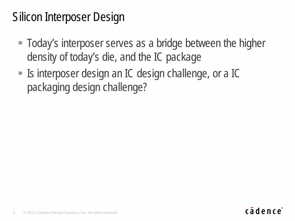
Silicon Interposer Design
Today’s interposer serves as a bridge between the higher density of today’s die, and the IC package Is interposer design an IC design challenge, or a IC
packaging design challenge?

3 © 2012 Cadence Design Systems, Inc. All rights reserved.
Interposer: Bridges IC and Package design
Interposer Features “Coarse” “Fine” Metal Line/Space > 5um/5um < 1um/1um Provider Package house, using
RDL manufacturing Foundry, using IC manufacturing
RDL Metal Cu Al, Cu RDL Thickness 3-5um <1um Passive Devices Yes Yes Cost Lower Higher Application Low I/O Count High I/O Count Design Rules Package-Like IC-Like Design Tool APD/SiP (EDI/VLE for
Validation) EDI/VLE (APD/SiP for Feasibility)

4 © 2012 Cadence Design Systems, Inc. All rights reserved.
“Classic” Interposer: Virtex-7 2000T
“Stacked Silicon Interconnect” 6.8 Billion transistors Four 28nm die on a “fine” Interposer
Source: Xilinx

5 © 2012 Cadence Design Systems, Inc. All rights reserved.
Silicon Interposer
Package Substrate
IC-Based 2.5D vs PKG-Based 2.5D
•IC Technology-Based Solution •Analysis include Core logic •Design for TEST •Timing Analysis (STA) •Manufacturing ready DRC •TSV implementation
•PKG/PCB Technology-Based Solution •System Interconnect Analysis •System Optimization thru all domains •Package Routing Technology •Core areas could be Black box •TSV proposal

6 © 2012 Cadence Design Systems, Inc. All rights reserved.
Perfect World: Interposer Design
IC-Tool-Based
PKG-Tool-Based
7 © 2012 Cadence Design Systems, Inc. All rights reserved.
Course PCB Rules
Fine IC Design Rules
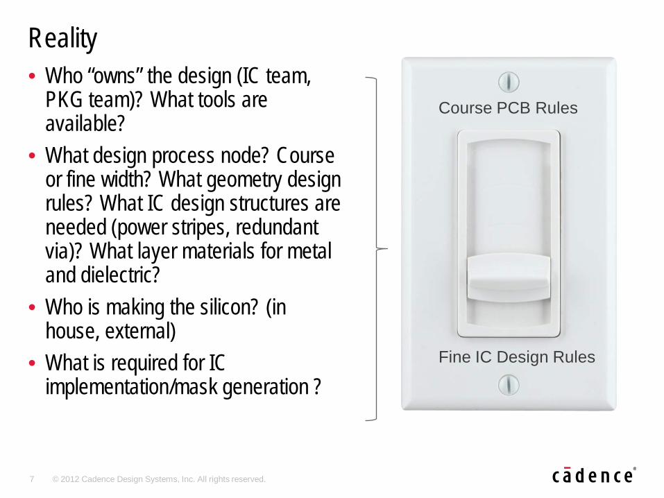
Reality • Who “owns” the design (IC team,
PKG team)? What tools are available?
• What design process node? Course or fine width? What geometry design rules? What IC design structures are needed (power stripes, redundant via)? What layer materials for metal and dielectric?
• Who is making the silicon? (in house, external)
• What is required for IC implementation/mask generation ?

8 © 2012 Cadence Design Systems, Inc. All rights reserved.
Why use Packaging tools for Si Interposer Planning?
• Sorting out the optimization
When considering fixed components on the board, the system (chip-interposer-package-board) can be optimized from the board up
• Preliminary system analysis
– When System route planning validates the route-ability of the system – System Signal and Power Integrity can be analyzed early
• Hand off the Interposer plan to IC tools
IC Packaging tools can create a representation of a silicon interposer that includes die placement, TSV locations, and feasibility routing that can be transferred to an IC tool for final detailed implementation using IC Design rules
9 © 2012 Cadence Design Systems, Inc. All rights reserved.
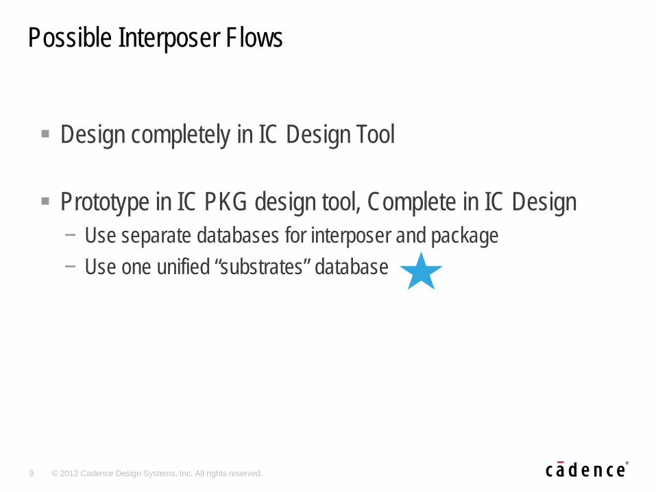
Possible Interposer Flows
Design completely in IC Design Tool Prototype in IC PKG design tool, Complete in IC Design − Use separate databases for interposer and package − Use one unified “substrates” database

10 © 2012 Cadence Design Systems, Inc. All rights reserved.
Common Database: Design Overview
interposer
logic mem Abstract#2: Front-side die pin
Abstract#1: Front-side die pin
Abstract#3: Back-side die pin
BGA
C4 bump
U-bump
package substrate
silicon substrate

11 © 2012 Cadence Design Systems, Inc. All rights reserved.
Interposer/Package Co-design Planning Flow
Die Abstract: Logic, Mem and Intpsr
Import Die abstract (distributed codesign)
PKG Tool
update
IC DesignTool
Add Package Component
Connectivity Manager
•Die to Die connectivity •Die to C4-bump connectivity •C4-bump to Ball connectivity
Connectivity Optimization (Auto assign Net…)
Routing(Auto/Interactive Route) •Die to Die Route •Die to C4-bump Route •C4-bump to Ball Route
GDSII for RDL on SiI Gerber on PKG
System Planner

12 © 2012 Cadence Design Systems, Inc. All rights reserved.
Co-Design and System Feasibility Planning
Bump Pattern Development 2.5D & 3D Planning IO Pad Ring Construction
Net Management System Connection Planning Multi-Die Support
Single Canvas Optimization of Chip-Interposer-Package-Board

13 © 2012 Cadence Design Systems, Inc. All rights reserved.
• IC technology information • Library
− I/O drivers − I/O pins
• Netlist − IC Net name inherited from
Verilog − Flight line between bumps
and I/O drivers • Physical
− Bumps − IC Cells/Pins − Die boundary
Die Abstract is Self-contained with …
14 © 2012 Cadence Design Systems, Inc. All rights reserved.
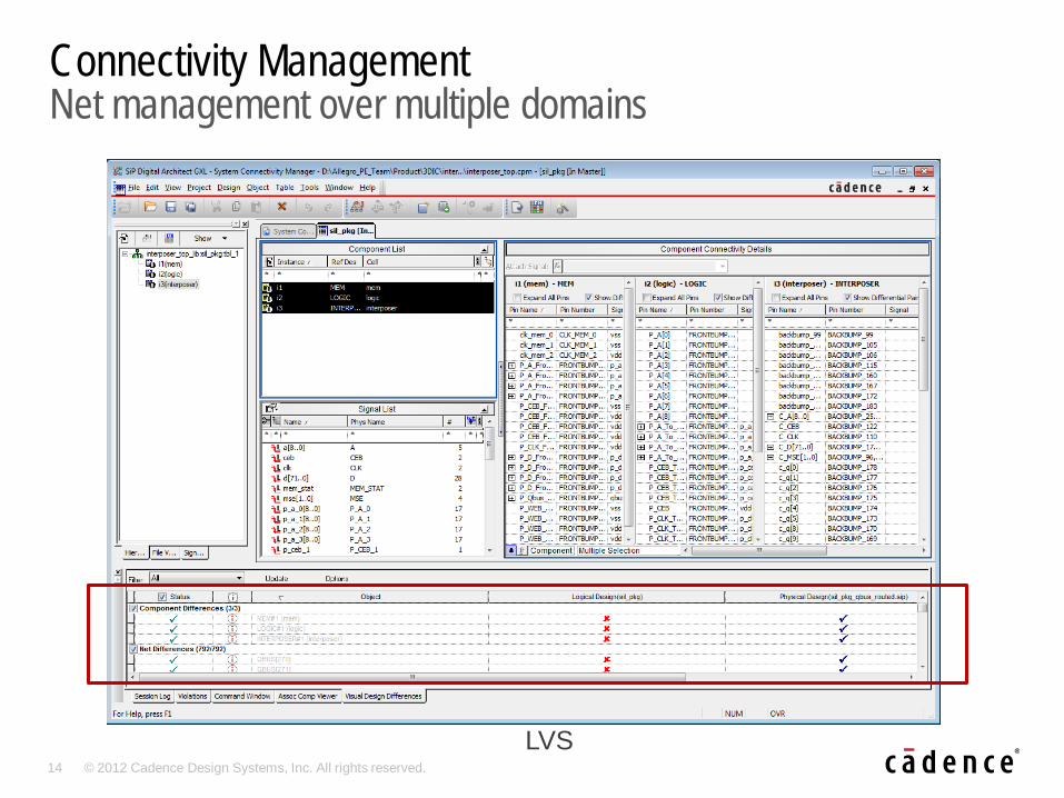
Connectivity Management Net management over multiple domains
LVS

15 © 2012 Cadence Design Systems, Inc. All rights reserved.
Automatic Die micro-bump Interposer C4-bump Package Ball Connection Optimization

16 © 2012 Cadence Design Systems, Inc. All rights reserved.
Bump and Micro-Bump Assignment Optimization
Before auto-assign net
After auto-assign net

17 © 2012 Cadence Design Systems, Inc. All rights reserved.
Auto RDL Routing Feasibility

18 © 2012 Cadence Design Systems, Inc. All rights reserved.
While optimizing bump to bump connection, micro-bump assignments in logic and memory die and C4-bump assignments in the interposer could change. Updated die abstract file and IO location file can be written to
update floor planning in IC tool.
Export Modified Bump Assignment back to IC Tool

19 © 2012 Cadence Design Systems, Inc. All rights reserved.
Export GDSII to combine RDL routing data in IC tool
Layer mapping between package & IC layout tool

20 © 2012 Cadence Design Systems, Inc. All rights reserved.
Extend Co-design into a “Single-Canvas View”
Generate netlist Create flat view of − PCB − Package/Interposer − IC
Optimize interfaces between fabrics
21 © 2012 Cadence Design Systems, Inc. All rights reserved.
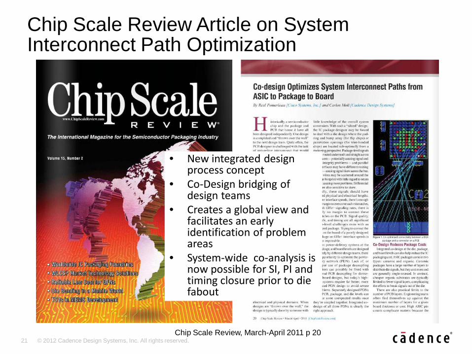
Chip Scale Review Article on System Interconnect Path Optimization
Chip Scale Review, March-April 2011 p 20
• New integrated design process concept
• Co-Design bridging of design teams
• Creates a global view and facilitates an early identification of problem areas
• System-wide co-analysis is now possible for SI, PI and timing closure prior to die fabout

22 © 2012 Cadence Design Systems, Inc. All rights reserved.
IC-IPSR-PKG-PCB Optimization
62 Ω 93 Ω 93 Ω
IO PKG PCB PKG IO
DDR DDR
Route Instantiation
Rats based Pin Assignment Throughout
Define routing path and sequencing

23 © 2012 Cadence Design Systems, Inc. All rights reserved.
Planner • Lightweight, rapid prototyping
environment for chip, package, board planning
System Planning & Single Canvas: Complementary Solutions
2
Plan Prototype Optimize Interconnect Implement Analyze &
Refine
Single Canvas • Detailed co-design
with greater awareness of constraints and routability

24 © 2012 Cadence Design Systems, Inc. All rights reserved.
Single-Canvas Extraction and Analysis
Leverage SI analysis tools with common view Co-simulation of chip-package-board system view − n-fabrics − n-layers − Board routing, package routing, RDL routing, vias

25 © 2012 Cadence Design Systems, Inc. All rights reserved.
Problem
• Lack of optimization between the Silicon Interposer and adjacent fabrics adds cost to the overall system and reduces system performance
Solution: Interposer planning
• A comprehensive system view and pin assignment optimization function will reduce the number of signal crossovers in the overall system
• System route feasibility and system SI and PI analysis validates that the Interposer will meet design specifications
Result
• A system optimized Silicon Interposer plan that can be handed off to IC implementation tools for final manufacturing prep
Package-Driven Si Interposer Benefits

26 © 2012 Cadence Design Systems, Inc. All rights reserved.


![High-Reliability Accelerometer and Pressure Sensor Design ...meptec.org/Resources/6 - Meggitt.pdf[1] “Practical Understanding of Key Accelerometer Specifications,” Technical Paper](https://static.documents.pub/doc/80x56/5eb59b3291cbaa59696a0fdf/high-reliability-accelerometer-and-pressure-sensor-design-meggittpdf-1.jpg)


![INVENTIVE - Si2projects.si2.org/events_dir/2007/date/cadence.pdf · INVENTIVE Common Power Format: ... ATPG Constraint Validation Equivalence checking ... [ -sdc_files sdc_file_list]](https://static.documents.pub/doc/80x56/5ac901cf7f8b9aa3298c99f7/inventive-common-power-format-atpg-constraint-validation-equivalence-checking.jpg)


