Simulation of Vector Mode Grating Coupler Interfaces for Integrated Optics Christopher T. Nadovich *1 , Derek J. Kosciolek 2 , William D. Jemison 1 and David T. Crouse 2 1 Clarkson University, 2 City University of New York *Corresponding author: [email protected]Abstract: The use of grating couplers to couple light near vertically in and out of optical slab or film waveguides represents an attractive method to interface optical fiber to photonic ICs. Newly developed fiber technologies exploiting vector mode polarization and orbital angular momentum (OAM) are inherently three- dimensional and interfaces for such beams require the solution of fully general 3D models, rather than the 2D models often used with ordinary grating couplers. In this work COMSOL Multiphysics was applied to the full 3D electromagnetic wave simulation of a novel forked grating coupler designed to interface with vortex modes of 1550 nm wavelength light. Full 3D models were solved for the radiating vector mode from a forked grating emitter structure driven from a nanophotonic waveguide. The results include interesting visualizations of vortex phasefronts, amplitude profiles, and polarization. Keywords: OAM, vortex, grating, photonics, optics. 1. Introduction The nature of the Forked Grating Coupler (FGC) device simulated herein ties together two distinct concepts: optical vorticies, and grating couplers for integrated optics. The following two sections provide a brief review of these topics. 1.1 Optical Vorticies Nye and Berry introduced the general theory of phase singularities in wave physics in 1974. In their seminal paper “Dislocations in Wave Trains” [1] they show that wavefronts can contain dislocation lines, closely analogous to those found in imperfect crystals. Surrounding these dislocations, the wave field can have interesting properties. Optical vortex (OV) beams [2] contain a wavefront phase singularity in their center. Such beams can propagate in free space or in special kinds of optical fiber waveguide. OV beams have a variety of potential applications in many areas, including particle manipulation [3], micro fabrication [4], and optical communications [5]. OV beams are characterized by helical phase fronts, a null central intensity, and the ability to convey internal optical orbital angular momentum (OAM) [6]. An important characteristic of of these beams is an azimuthal phase dependence e iχφ where φ is the azimuthal angle about the beam, and χ represents the overall topological charge of the internal Orbital Angular Momentum (OAM) of the beam. As a consequence of this helical phase, the phase front has a screw dislocation in the center of the beam. E fields cancel at this point giving rise to so called “donut modes” with zero intensity centers and singular phase. These properties of OAM beams are illustrated in Figure 1. Figure 1. Magnitude (left) and phase of χ = +1 vortex beam cross section. The specific advantage possessed by OV beams for use in communications is that they can be described as the superposition of infinite set of mutually orthogonal propagating modes that are independent of polarization and wavelength. As these orthogonal OAM modes are parameterized by the distinct integer “topological charge” that can vary without theoretical limit, exploiting OAM can multiply the number of available channels in optical communications multiplexing above and beyond what is available with wavelength and polarization multiplexing [5]. Many methods for generating and manipulating vortex beams have been developed. Of particular Excerpt from the Proceedings of the 2015 COMSOL Conference in Boston
Transcript
Simulation of Vector Mode Grating Coupler Interfaces for Integrated Optics Christopher T. Nadovich*1, Derek J. Kosciolek2, William D. Jemison1 and David T. Crouse2 1Clarkson University, 2City University of New York *Corresponding author: [email protected] Abstract: The use of grating couplers to couple light near vertically in and out of optical slab or film waveguides represents an attractive method to interface optical fiber to photonic ICs. Newly developed fiber technologies exploiting vector mode polarization and orbital angular momentum (OAM) are inherently three-dimensional and interfaces for such beams require the solution of fully general 3D models, rather than the 2D models often used with ordinary grating couplers. In this work COMSOL Multiphysics was applied to the full 3D electromagnetic wave simulation of a novel forked grating coupler designed to interface with vortex modes of 1550 nm wavelength light. Full 3D models were solved for the radiating vector mode from a forked grating emitter structure driven from a nanophotonic waveguide. The results include interesting visualizations of vortex phasefronts, amplitude profiles, and polarization. Keywords: OAM, vortex, grating, photonics, optics. 1. Introduction The nature of the Forked Grating Coupler (FGC) device simulated herein ties together two distinct concepts: optical vorticies, and grating couplers for integrated optics. The following two sections provide a brief review of these topics. 1.1 Optical Vorticies Nye and Berry introduced the general theory of phase singularities in wave physics in 1974. In their seminal paper “Dislocations in Wave Trains” [1] they show that wavefronts can contain dislocation lines, closely analogous to those found in imperfect crystals. Surrounding these dislocations, the wave field can have interesting properties. Optical vortex (OV) beams [2] contain a wavefront phase singularity in their center. Such beams can propagate in free space or in special
kinds of optical fiber waveguide. OV beams have a variety of potential applications in many areas, including particle manipulation [3], micro fabrication [4], and optical communications [5]. OV beams are characterized by helical phase fronts, a null central intensity, and the ability to convey internal optical orbital angular momentum (OAM) [6]. An important characteristic of of these beams is an azimuthal phase dependence eiχφ where φ is the azimuthal angle about the beam, and χ represents the overall topological charge of the internal Orbital Angular Momentum (OAM) of the beam. As a consequence of this helical phase, the phase front has a screw dislocation in the center of the beam. E fields cancel at this point giving rise to so called “donut modes” with zero intensity centers and singular phase. These properties of OAM beams are illustrated in Figure 1.
Figure 1. Magnitude (left) and phase of χ = +1 vortex beam cross section. The specific advantage possessed by OV beams for use in communications is that they can be described as the superposition of infinite set of mutually orthogonal propagating modes that are independent of polarization and wavelength. As these orthogonal OAM modes are parameterized by the distinct integer “topological charge” that can vary without theoretical limit, exploiting OAM can multiply the number of available channels in optical communications multiplexing above and beyond what is available with wavelength and polarization multiplexing [5]. Many methods for generating and manipulating vortex beams have been developed. Of particular
Excerpt from the Proceedings of the 2015 COMSOL Conference in Boston
significance to this work are the vortex generation methods based on forked holograms. If an ordinary Bragg diffraction grating (of either phase or amplitude) is modified (forked) to include an edge dislocation at its center, then the first-order diffracted beam contains an optical vortex singularity [7]. 1.2 Grating Couplers The technology to connect external electronic signals carried by copper PCB traces to ordinary electronic ICs is straightforward and well established. An electronic signal is conducted from the PCB trace through an IC package pin to the internal lead frame and on through bond wires welded to metalized pads on the IC perimeter. In contrast, technology for connecting external photonic signals, free space or fiber-guided light beams, to a Photonic IC (PIC) is not quite as straightforward. Nevertheless several viable fiber-to-PIC interface options have emerged [8], including
Of these options, the use of grating couplers is becoming a very well developed technology with many advantages over the other techniques [9]. These so called “Bragg couplers” couple light near vertically in and out of the optical slab or film waveguides of integrated optics. Theoretical efficiencies for optimized grating couplers approach 100% and practical implementations have demonstrated efficiencies over 60% [10]. The near vertical coupling of a grating coupler provides physical flexibility in placing the optical interface anywhere on the chip surface. As such, a grating coupler represents an analogous optical “bond pad” on the PIC where a fiber conveniently could be butt-coupled, or a free-space beam could be focused. This allows increasing the density of optical interfaces and preserves the chip edge to be used for low- and high-speed electronic signal pads. 1.3 The Forked Grating Coupler
The novel Forked Grating Coupler (FGC) invention [11, 12] applies a forked grating structure to the design of the diffracting “lines” in an integrated optics grating coupler in order to make the device compatible with vortex light beams. These “lines,” which may be grooves, or ridges, or a photonic metamaterial discontinuity arranged in a smooth curve, follow the forked diffraction pattern lobes over a 2D surface. An example forked grating using constant width grooves is shown in Figure 2.
Figure 2. Forked grating for χ = +1
The resulting device can absorb or radiate a vortex beam mode at near-normal incidence to a PIC and transform that vortex mode to a TE or TM waveguide mode traveling along a slab or strip optical waveguide parallel to the surface of the IC.
Figure 3. Forked grating coupler device component parts. A sketch of a FGC fabricated on a Silicon-on-Insulator (SOI) wafer is shown in Figure 3. A 220 nm thick top “device layer” of silicon is etched away around the perimeter of the device, leaving the buried oxide (SiO2) exposed as an outline. This outlining etch defines the 450x220 nm input/output photonic “wire” waveguide that
Excerpt from the Proceedings of the 2015 COMSOL Conference in Boston
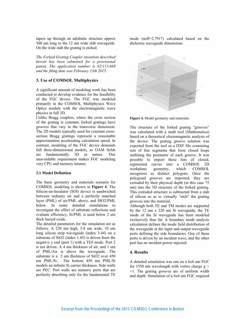
tapers up through an adiabatic structure approx 500 um long to the 12 um wide slab waveguide. On the wide slab the grating is etched. The Forked Grating Coupler invention described herein has been submitted for a provisional patent. The application number is 62/115,668 and the filing date was February 13th 2015. 3. Use of COMSOL Multiphysics A significant amount of modeling work has been conducted to develop evidence for the feasibility of the FGC device. The FGC was modeled primarily in the COMSOL Multiphysics Wave Optics module with the electromagnetic wave physics in full 3D. Unlike Bragg couplers, where the cross section of the grating is constant, forked gratings have grooves that vary in the transverse dimension. The 2D models typically used for constant cross-section Bragg gratings represent a reasonable approximation accelerating calculation speed. In contrast, modeling of the FGC device demands full three-dimensional models, as OAM fields are fundamentally 3D in nature. This unavoidable requirement makes FGC modeling very CPU and memory intense. 3.1 Model Definition The basic geometry and materials scenario for COMSOL modeling is shown in Figure 4. The Silicon-on-Insulator (SOI) device is sandwiched between ordinary air and a perfectly matched layer (PML) of air/PML above, and SIO2/PML below. In some detailed simulations to investigate the effect of substrate reflections and evaluate efficiency, Si/PML is used below 2 um thick buried oxide. The detailed parameters for the simulation are as follows. A 220 nm high, 5.8 um wide, 10 um long silicon strip waveguide (index 3.44) on a substrate of SiO2 (index 1.45) is driven from the negative y end (port 1) with a TE0 mode. Port 2 is not driven. A 4 um thickness of air, and 1 um of PML/Air is above the waveguide. The substrate is a 2 um thickness of SiO2 over 450 nm PML/Si. The bottom 450 nm PML/Si models an infinite Si carrier thickness. Side walls are PEC. Port walls are numeric ports that are perfectly absorbing only for the fundamental TE
mode (neff=2.7917) calculated based on the dielectric waveguide dimensions.
Figure 4. Model geometry and materials. The structure of the forked grating “grooves” was calculated with a math tool (Mathematica) based on a theoretical electomagnetic analysis of the device. The grating groove solution was exported from the tool as a DXF file containing sets of line segments that form closed loops outlining the perimeter of each groove. It was possible to import these lists of closed, segmented curves into a COMSOL 2D workplane geometry, which COMSOL recognizes as distinct polygons. Once the polygonal grooves are imported, they are extruded by their physical depth (in this case 75 nm) into the 3D structure of the forked grating. This extruded structure is subtracted from a slab of silicon so as to virtually “etch” the grating grooves into the material. Although both TE and TM modes are supported by the 12 um x 220 nm Si waveguide, the TE mode of the Si waveguide has been modeled exclusively thus far. A boundary mode analysis calculation defines the mode field distribution of the waveguide at the input and output waveguide ports defining the side boundaries. One of these ports is driven by an incident wave, and the other port has no incident power injected. 4. Results A detailed simulation was run on a 6x6 um FGC for 1550 nm wavelength with vortex charge χ = +1. The grating grooves are of uniform width and depth. Simulation of a 6x6 um FGC required
Excerpt from the Proceedings of the 2015 COMSOL Conference in Boston
approximately 75 GB RAM and took 45 minutes to run on a 16 core 2.8 Ghz computer. 4.1 Visualization
Figure 5. Isosurface plot of electric field for phase=0. An animated version may be viewed at the URL http://nadovich.com/vortex.gif A 3D isosurface plot in Figure 5 shows the vortex phase=0 front emerging from the forked grating. A cylindrical data filter is added to the visualization node in COMSOL to better see the “corkscrew phase” section of the beam. One of the unique characteristics of a vortex beam is that the Poynting vector has an azimuthal component. This component is responsible for the orbital angular momentum carried by the beam. A visualization of the Poynting vector streamlines that illustrates the azimuthal component is shown in Figure 6.
Figure 6. Poynting vector streamlines
Transverse (P-plane) cuts through the center of the device are shown in Figure 7 (amplitude) and Figure 8 (wave E-field x-component). The “themal” color scheme seemed most appropriate for unipolar magnitude, while the “wave” scheme facilitates visualization of bipolar real values like the E-field x-component.
Figure 7. Annotated P-plane cut of electric field norm.
Figure 8. Annotated P-plane cut of E-field x component. Vague standing waves are observable in the output (Port 2) waveguide and output-side of the beam. This possibly could be explained by higher order modes propagating toward Port 2 that are reflected rather than absorbed by the numeric port. To study this amplitude asymmetry in the beam more closely, consider Figure 9 showing a tilted beam cut plane at 2 um height, tilted 9.4 degrees to be exactly transverse to the beam axis.
Excerpt from the Proceedings of the 2015 COMSOL Conference in Boston
Figure 9. Cut plane transverse to the beam. Seen in plan view in Figure 10 an amplitude imbalance toward the y < 0 side (the Port 1 input side) is evident. The imbalance is approximately 6 dB. Compare this imbalance with the overall 7.5 dB loss through the device (S21). Amplitude non-uniformity is expected in a grating coupler with uniform groove width across the face of the grating. Constant groove width creates a constant attenuation factor, α, in the waveguide mode and the radiated amplitude of the leaky wave decays exponentially.
Figure 10. Electric field norm plotted on beam cut plane The waveguide mode is the fundamental TE mode with the E vector along the x axis, and the grating lines are largely parallel to the x axis, so we would expect the resulting radiation to be polarized along the x axis as well. This expected polarization is proved in Figure 11. The norm of the E vector is almost indistinguishable from the Ex component.
Figure 11. Beam cuts in different polarizations. 4.2 Quantitative Performance The quantitative device performance predicted by the COMSOL global post-processing calculations is as follows:
Beam tilt error: +1.4 degrees S11: -15.8 dB S21: -7.5 dB Central null offset: -210 nm Conjugate OAM Mode Crosstalk:
-13.2 dB
Oveall power efficiency: 31.8% Global calculations of S-parameters are built in COMSOL global evaluation options. To facilitate calculation of beam metrics, integration disks above the device were included in the model geometry. These disks were used for integrations to compute overlap integrals yielding efficiency and crosstalk measurements. COMSOL also calculated beam-pointing error. This grating was designed to implement an 8º beam axis tilt based on an assumption of an effective index under the grating of 2.63. COMSOL integrated the arc tangent of the y and z Poynting vector components on a 2 um radius circle at 1 um height over the center of the grating, we obtain an averaged beam angle in the simulation of 9.4º. To confirm conservation of power, integrate the Poynting vector over the top and bottom surfaces (the Air – Air/PML interface, and the SiO2 – Si/PML interface). The results from the simulation are:
PIN Incident Port 1 Power
1.0 W
PREF Reflected Power (Port 1)
0.026W
PTX Transmitted Power (Port 2)
0.178 W
PUP Total Upward Beam Power
0.435 W
PDN Total Downward Substrate Power
0.347 W
POUT = PREF+PTX+PUP+PDN
Total Scattered Power
0.984 W
PIN – POUT “Lost” Power 0.016 W
Excerpt from the Proceedings of the 2015 COMSOL Conference in Boston
There is small 0.016 Watt unaccounted for in the conservation of power assessment. This is not unexpected for a lambda/5 COMSOL simulation mesh and a convergence limit of 0.01. A finer mesh and tighter convergence limit in the simulation might provide a more accurate energy balance at the cost of a significantly longer run time and memory requirement. Integrating just the outflow power up through a disk of 3 um radius tilted at 9.4 degrees and centered on the beam null yields 0.408 Watt The above number might suggest that the coupler has 40.8% efficiency, but this is not nearly the case. The mode pattern radiated upward will not perfectly match a Charge = +1 OAM mode. To evaluate how well the OV beam will couple from a vortex fiber to the forked grating coupler, an overlap integral is typically used to calculate the coupling factor. One such possible integral is The calculated Mode Coupling Overlap Integral Power Efficiency based on an integration over a 3 um radius disk aligned with the beam against various OAM Charges (χ) modeled as ideal Bessel Gaussian beams is
The “best” coupling, by far, occurs at the desired charge = -1. The coupler forked grating was designed for +1 charge in detector mode. The simulation was done in emitter mode, which explains the flip in sign. Given the total power through the integration disk is 0.408 watt, and the mode coupling efficiency is 78%, an overall power transfer efficiency of 31.8% is predicted (neglecting reflections at the fiber facet). This efficiency is commensurate with efficiencies achieved by basic non-vortex Bragg couplers. 5. Conclusions The simulation results from COMSOL give us good assurance that the Forked Grating Coupler device can emit vortex beams of the desired
topological charge. This assurance has given us confidence to proceed forward with fabrication of the FGC in silicon. Fabrication is underway now and measured results will soon be available for comparison with the COMSOL calculated results. 6. References [1] Nye, J. F. and Berry, M.V., Dislocations in Wave Trains. Proceedings of the Royal Society A, 1974. [2] Andrews D., Structured Light and Its Applications, Academic Press, 2008. [3] GarcésChávez, et al, “Observation of the Transfer of the Local Angular Momentum Density of a Multiringed Light Beam to an Optically Trapped Particle.” Physical Review Letters, 91 (9): 093602, 2003. [4] Hamazaki, Junichi et al, “OpticalVortex Laser Ablation.” Optics Express 18 (3): 2144–51, 2010. [5] Bozinovic, Nenad, et al, “TerabitScale Orbital Angular Momentum Mode Division Multiplexing in Fibers.” Science 340 (6140): 1545–48, 2013. [6] Alison M. Yao and Miles J. Padgett, “Orbital angular momentum: origins, behavior and applications”, Advances in Optics and Photonics 3, 161204, 2011. [7] Li, Yanming, et al, “Orbital Angular Momentum Generation and Mode Transformation with High Efficiency Using Forked Polarization Gratings.” Applied Optics 51 (34): 8236–45, 2012. [8] Hunsperger, R. G., Integrated Optics: Theory and Technology, Springer, 2009. [9] Taillaert, Dirk, et al, “Grating Couplers for Coupling between Optical Fibers and Nanophotonic Waveguides.” Japanese Journal of Applied Physics 45 (8A): 6071–77, 2006. [10] Antelius, M., et al, “An apodized SOI waveguide to fiber surface grating coupler for single lithography silicon photonics”, Optics Express, 19(4), 3592–3598, 2007. [11] C. T. Nadovich, et al, “Forked grating coupler optical vortex beam interface for integrated optics”, presented at the Third International Conference on Optical Angular Momentum, New York, N.Y., 2015. [12] D.J Kosciolek, et al, “SOI Forked Grating Coupler for Integrated Optics: Fabrication
Excerpt from the Proceedings of the 2015 COMSOL Conference in Boston
Tolerances and Efficiency Improvements for Coupling into a Single Mode Fiber”, presented at META’15, the 6th International Conference on Metamaterials, Photonic Crystals and Plasmonics, New York, N.Y., 2015. 7. Acknowledgements
This work is supported by the NSF Center for Metamaterials I/UCRC and Corning Incorporated.
Excerpt from the Proceedings of the 2015 COMSOL Conference in Boston