1 The DSP Primer Presented by: Bob Stewart University of Strathclyde, Scotland, UK [email protected]Steve Alexander University of Strathclyde, Scotland, UK [email protected]Jeff Weintraub Xilinx Inc, San Jose, USA [email protected]Presented as part of Xilinx University Program (XUP) August 2005, Version 0.97
8.1 CIC filters 579 Direct Digital Downconversion 61
9.1 Downconversion using DSP 619.2 CICs for Downconversion 64
10 Numerically Controlled Oscillators 6610.1 Look-up Table Technique 6610.2 Sine Wave Generation Using IIR Filters 68
11 CORDIC - Vector Magnitude Calculations. 7411.1 The Golden Reference Design 7411.2 The Fixed Point CORDIC Design 7511.3 Build A Fixed Point CORDIC System. 8111.4 Using CORDIC In A QR-Array 82
12 Fixed Point Sigma-Delta 8513 Fixed Point Bandlimiting: RRC Filtering 8614 FPGA as an ASIC - Digital Downconverter 89
4
51 Introduction
1 Introduction
In this DSP for FPGAs Primer workbook the aim is:
• To allow all users experience of using the entire toolchain from DSPalgorithm concept to FPGA implementation.
After completing this workbook you will be able to:
• Understand fundamental DSP algorithms for FPGA implementation;• Be aware of the FPGA hardware for implementation of DSP algorithms;• Know how to use Simulink and SystemGenerator for the simulation of DSP
algorithms, architectures and systems• Know how to correctly design a DSP system with knowledge of issues
relating to wordlengths, overflow, saturation, wraparound and so on.• Be able to take a design from Simulink System Generator implementation to
Xilinx ISE tools.• Know how to use Xilinx ISE tools to synthesize and place and route the
design.• Know how to use the Xilinx FPGA editor to inspect the actual hardware
implementation with respect to on-chip hardware.• Know how to perform hardware-in-the-loop simulation.• Know how to run DSP algorithms on the XUP Virtex 2 Pro board.
1.1 Software Required
The following software is required to complete the various examples in thisworkbook:
1. MatLab Release 14, Simulink 62. Xilinx System Generator v7.13. Xilinx ISE Tools v7.1 + ServicePack 3 + IP update;4. Xilinx Chipscope v7.1
If any of these are missing please contact the appropriate vendor for install filesand a licence.
We will be using Xilinx ISE tools for synthesis and HDL simulation. It is ofcourse possible to use other synthesis tools (Leonardo, Synplicity) to do thesestages.
6
1.2 Example Files and Directories
The examples for this workbook should be copied to the location:
c:\Xilinx_DSP_PrimerAs a short cut notation we will use the Xilinx symbol to specify the directoryc:\Xilinx_DSP_PrimerYou will note that all top level Simulink models (with the.mdl suffix) are usuallylocated in a directory with the same name. For example the Simulink modelshortfilter.mdl would be found in directory:
\shortfilter\shortfilter.mdlor
c:\Xilinx_DSP_Primer\shortfilter\shortfilter.mdlThe reason for placing the examples in their own named directory is to ensurethat if you decide to set up a Xilinx ISE project file, then there is no interactionor mixing of different ISE project files which could happen if the ISE tools wereused on two or more different .mdl files in the same directory.
1.3 Shorthand for Mouse Clicks
Shorthand symbols for mouse clicks will be used in this workbook according tothe table below:
2 Top-Level View of the Design Flow
In this section we take some very simple designs through the entire design flowfrom simulation to bitstream form ready for implementation on an FPGA.
2 1
H
1 Left mouse button click once
Right mouse button click onceLeft mouse button click twice
Left mouse button hold down Right mouse button hold downH
Figure 1.1: Mouse and keyboard click notation used in this document.
Right mouse button click once2
72 Top-Level View of the Design Flow
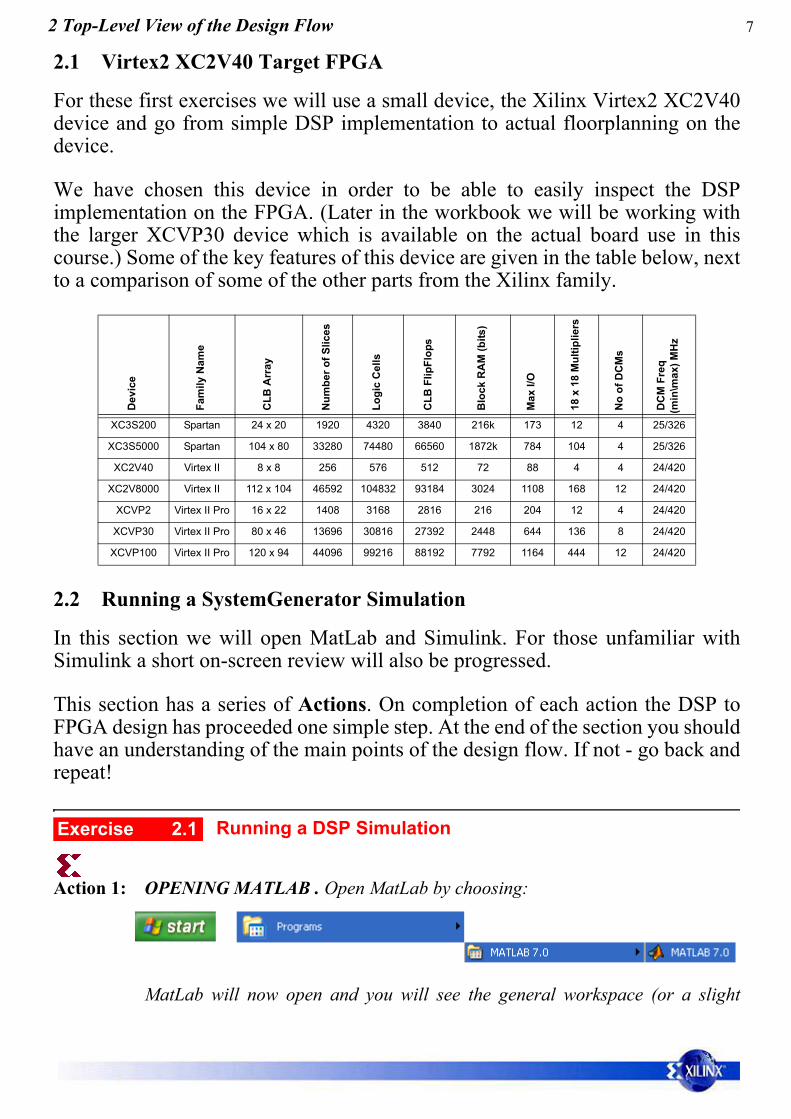
2.1 Virtex2 XC2V40 Target FPGA
For these first exercises we will use a small device, the Xilinx Virtex2 XC2V40device and go from simple DSP implementation to actual floorplanning on thedevice.
We have chosen this device in order to be able to easily inspect the DSPimplementation on the FPGA. (Later in the workbook we will be working withthe larger XCVP30 device which is available on the actual board use in thiscourse.) Some of the key features of this device are given in the table below, nextto a comparison of some of the other parts from the Xilinx family.
2.2 Running a SystemGenerator Simulation
In this section we will open MatLab and Simulink. For those unfamiliar withSimulink a short on-screen review will also be progressed.
This section has a series of Actions. On completion of each action the DSP toFPGA design has proceeded one simple step. At the end of the section you shouldhave an understanding of the main points of the design flow. If not - go back andrepeat!
Running a DSP Simulation
Action 1: OPENING MATLAB . Open MatLab by choosing:
MatLab will now open and you will see the general workspace (or a slight
XC2V40 Virtex II 8 x 8 256 576 512 72 88 4 4 24/420
XC2V8000 Virtex II 112 x 104 46592 104832 93184 3024 1108 168 12 24/420
XCVP2 Virtex II Pro 16 x 22 1408 3168 2816 216 204 12 4 24/420
XCVP30 Virtex II Pro 80 x 46 13696 30816 27392 2448 644 136 8 24/420
XCVP100 Virtex II Pro 120 x 94 44096 99216 88192 7792 1164 444 12 24/420
Exercise 2.1
8
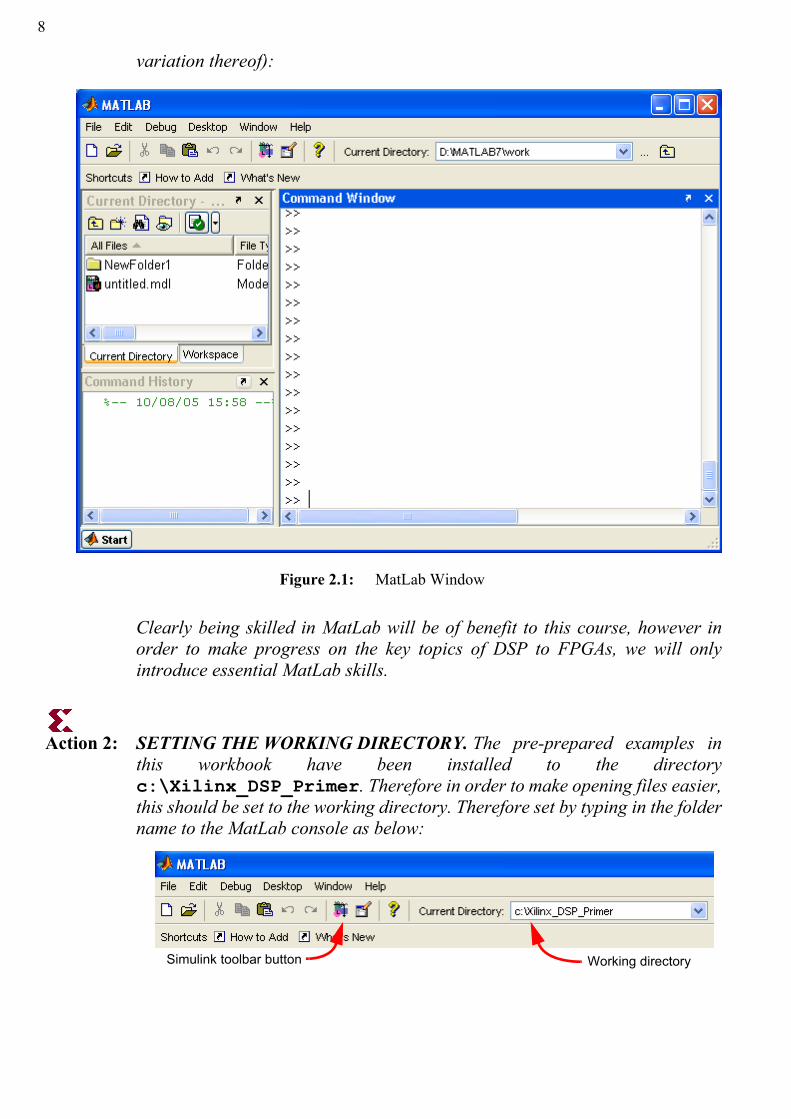
variation thereof):
Clearly being skilled in MatLab will be of benefit to this course, however inorder to make progress on the key topics of DSP to FPGAs, we will onlyintroduce essential MatLab skills.
Action 2: SETTING THE WORKING DIRECTORY. The pre-prepared examples inthis workbook have been installed to the directoryc:\Xilinx_DSP_Primer. Therefore in order to make opening files easier,this should be set to the working directory. Therefore set by typing in the foldername to the MatLab console as below:
Figure 2.1: MatLab Window
Simulink toolbar button Working directory
92 Top-Level View of the Design Flow
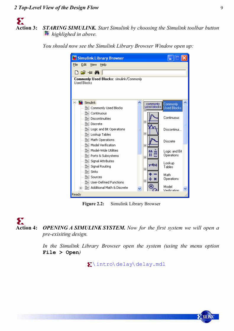
Action 3: STARING SIMULINK. Start Simulink by choosing the Simulink toolbar button highlighed in above.
You should now see the Simulink Library Browser Window open up:
Action 4: OPENING A SIMULINK SYSTEM. Now for the first system we will open apre-exisiting design.
In the Simulink Library Browser open the system (using the menu optionFile > Open)
\intro\delay\delay.mdl
Figure 2.2: Simulink Library Browser
10
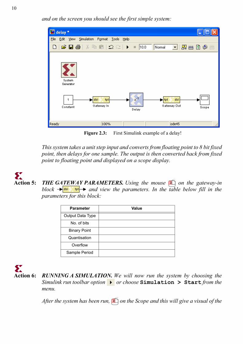
and on the screen you should see the first simple system:
This system takes a unit step input and converts from floating point to 8 bit fixedpoint, then delays for one sample. The output is then converted back from fixedpoint to floating point and displayed on a scope display.
Action 5: THE GATEWAY PARAMETERS. Using the mouse on the gateway-inblock and view the parameters. In the table below fill in theparameters for this block:
Action 6: RUNNING A SIMULATION. We will now run the system by choosing theSimulink run toolbar option or choose Simulation > Start from themenu.
After the system has been run, on the Scope and this will give a visual of the
Parameter Value
Output Data Type
No. of bits
Binary Point
Quantisation
Overflow
Sample Period
Figure 2.3: First Simulink example of a delay!
2
2
112 Top-Level View of the Design Flow
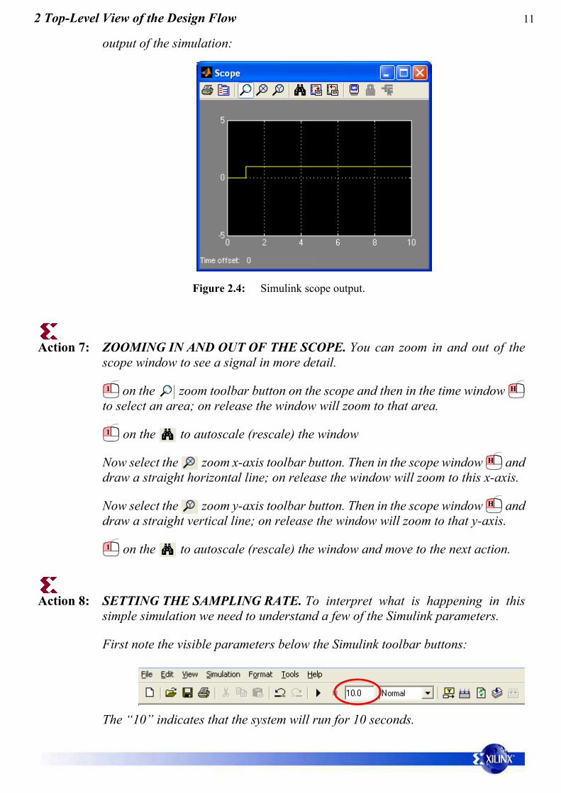
output of the simulation:
Action 7: ZOOMING IN AND OUT OF THE SCOPE. You can zoom in and out of thescope window to see a signal in more detail.
on the zoom toolbar button on the scope and then in the time window to select an area; on release the window will zoom to that area.
on the to autoscale (rescale) the window
Now select the zoom x-axis toolbar button. Then in the scope window anddraw a straight horizontal line; on release the window will zoom to this x-axis.
Now select the zoom y-axis toolbar button. Then in the scope window anddraw a straight vertical line; on release the window will zoom to that y-axis.
on the to autoscale (rescale) the window and move to the next action.
Action 8: SETTING THE SAMPLING RATE. To interpret what is happening in thissimple simulation we need to understand a few of the Simulink parameters.
First note the visible parameters below the Simulink toolbar buttons:
The “10” indicates that the system will run for 10 seconds.
Figure 2.4: Simulink scope output.
1 H
1
H
H
1
12
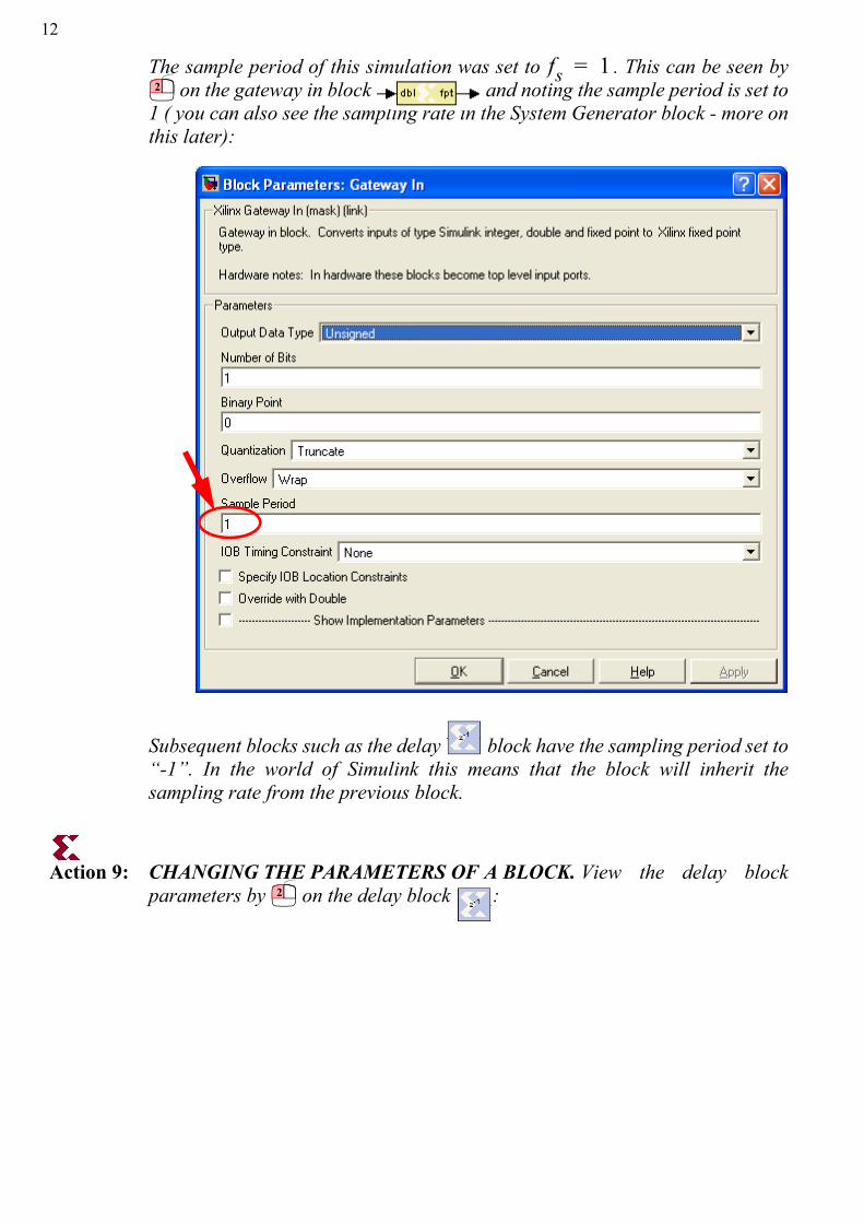
The sample period of this simulation was set to . This can be seen by on the gateway in block and noting the sample period is set to
1 ( you can also see the sampling rate in the System Generator block - more onthis later):
Subsequent blocks such as the delay block have the sampling period set to“-1”. In the world of Simulink this means that the block will inherit thesampling rate from the previous block.
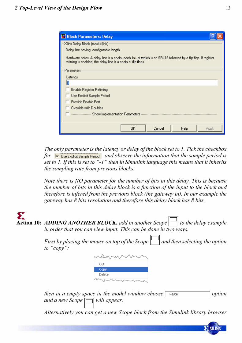
Action 9: CHANGING THE PARAMETERS OF A BLOCK. View the delay blockparameters by on the delay block :
fs 1=2
2
132 Top-Level View of the Design Flow
The only parameter is the latency or delay of the block set to 1. Tick the checkboxfor and observe the information that the sample period isset to 1. If this is set to “-1” then in Simulink language this means that it inheritsthe sampling rate from previous blocks.
Note there is NO parameter for the number of bits in this delay. This is becausethe number of bits in this delay block is a function of the input to the block andtherefore is infered from the previous block (the gateway in). In our example thegateway has 8 bits resolution and therefore this delay block has 8 bits.
Action 10: ADDING ANOTHER BLOCK. add in another Scope to the delay examplein order that you can view input. This can be done in two ways.
First by placing the mouse on top of the Scope and then selecting the optionto “copy”:
then in a empty space in the model window choose optionand a new Scope will appear.
Alternatively you can get a new Scope block from the Simulink library browser
14
(see Figure 2.2 on page 9) and select from the option:
and select Scope and the scope into the Simulink workspace and dropwhere you want to place the scope.
Action 11: CONNECTING BLOCKS TOGETHER. You should now have a system withan additional scope similar to below:
If you want to move any block then on the block and drag and drop to whereyou want to put it.
To connect the new scope block place the mouse on top of the actual “wire”connection and at position and observe the mouse pointer change tocrosshairs ; then (still holding the right mouse button down) drag to connectto the > at position - when you are at the connection point observe that thecross-hairs become double now let go of the mouse button.
You should now have successfully connected the constant to the scope as below!
Action 12: DISCONNECTING BLOCKS. To disconnect the connection just made,highlight the connecting line of interest at position by and note that theline is now selected. You can then either hit BACKSPACE on the keyboard, or
and select .
H
1
2
H
H 1
2
3
4
3 1
1
152 Top-Level View of the Design Flow
Reconnecting the line using the procedure from the previous Action.
Action 13: RECONNECTING BLOCKS. Disconnect the two blocks at position bydeleting the wire. Note that to connect two blocks (i.e. not tapping off an exisitingconnection as in Action 11) you simply select the “from” block “>” (on the rightside) and then drag and hold to connect to the “>” on the “destination”block.
Before proceeding ensure all disconnections are remade and continue.
Action 14: RE-RUNNING THE SYSTEM. Run the system with the added scope. Openboth scopes by on each scope. Observe that the output is in fact a delayedversion of the input with a single sample delay, and a sampling rate of 1Hz.
Modifying Time Parameters of a Simulink Simulation Open the system:
\intro\delay2\delay2.mdl(This is the same system that would be generated by completing all of theAction 1 to Action 14 on the delay.mdl file.)(a) Run the system and confirm a sampling rate of 1Hz, and a single 8 bit
sample delay.(b) Change the sample rate of the system to 100Hz by modifying the sample
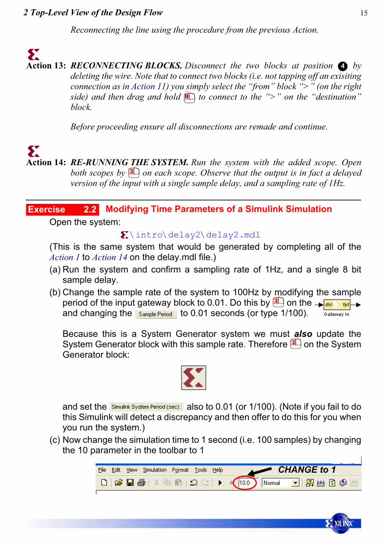
period of the input gateway block to 0.01. Do this by on the and changing the to 0.01 seconds (or type 1/100).
Because this is a System Generator system we must also update theSystem Generator block with this sample rate. Therefore on the SystemGenerator block:
and set the also to 0.01 (or 1/100). (Note if you fail to dothis Simulink will detect a discrepancy and then offer to do this for you whenyou run the system.)
(c) Now change the simulation time to 1 second (i.e. 100 samples) by changingthe 10 parameter in the toolbar to 1
4
H
2
Exercise 2.2
2
2
CHANGE to 1
16
(d) Run the system and then observe the two scopes. You should see 100samples, and still a delay of 1 sample. The time axis on the scopes shouldnow reflect that the simulation was performed at a sampling rate of
.
Modifying Block Functionality in a Simulink SimulationOpen the system:
\intro\delay3\delay3.mdlThis system has sampling rate set to and will run for 0.02seconds or 200 samples. In this example we will change the input signal to asine wave and then change the parameters of the delay block.
(a) First delete the constant source by on the block and selecting. Note that the now unconnected wires remain but are
highlighted red and are dotted indicating they are free-floating and notconnected.
(b) Goto the browser window and find the sources and view the sources set of blocks.
Scroll down to find the sine wave and then into the exampleworkspace and place carefully just at the the end of the red line where theprevious source was. This should then make the connections as werepreviously set. If the connections are not made for you, simply place thesine wave and then manually make the connections according to theprocedures described earlier in Action 11 (page 14) and Action 13(page 15).
(c) On the sine wave now on the parameter dialog, change the to 50
and to 2*pi*100
Note that the frequency parameter is in radians/sec hence to convert to Hzwe simply multiply by 2π. In Simulink just type “pi” for π and “*” for multiply.
fs 100=
Exercise 2.3
fs 10000Hz=
1
H
2
172 Top-Level View of the Design Flow
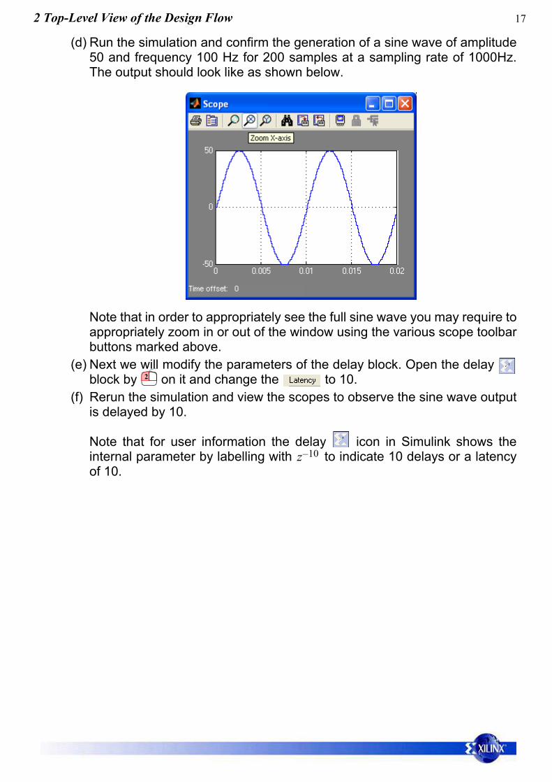
(d) Run the simulation and confirm the generation of a sine wave of amplitude50 and frequency 100 Hz for 200 samples at a sampling rate of 1000Hz.The output should look like as shown below.
Note that in order to appropriately see the full sine wave you may require toappropriately zoom in or out of the window using the various scope toolbarbuttons marked above.
(e) Next we will modify the parameters of the delay block. Open the delay block by on it and change the to 10.
(f) Rerun the simulation and view the scopes to observe the sine wave outputis delayed by 10.
Note that for user information the delay icon in Simulink shows theinternal parameter by labelling with to indicate 10 delays or a latencyof 10.
2
z 10–
18
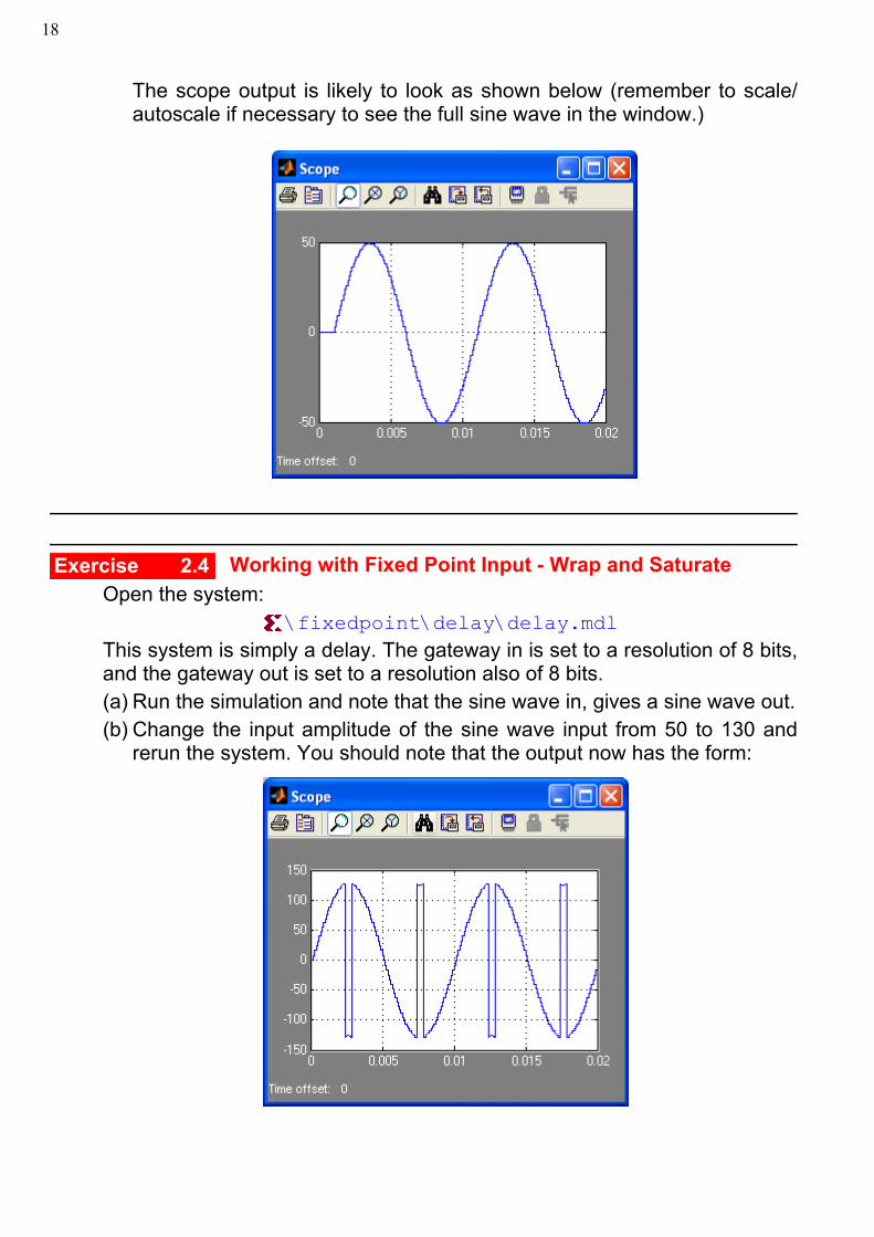
The scope output is likely to look as shown below (remember to scale/autoscale if necessary to see the full sine wave in the window.)
Working with Fixed Point Input - Wrap and SaturateOpen the system:
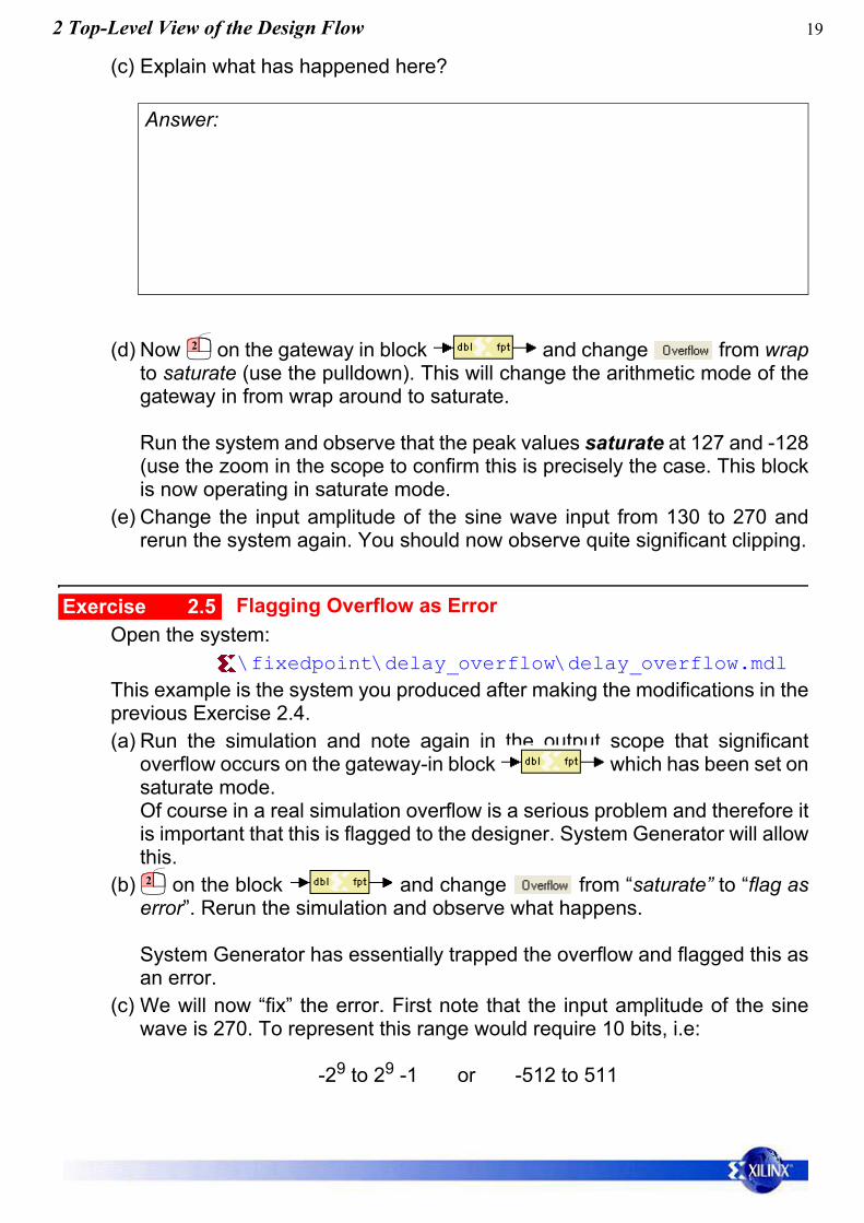
\fixedpoint\delay\delay.mdlThis system is simply a delay. The gateway in is set to a resolution of 8 bits,and the gateway out is set to a resolution also of 8 bits.(a) Run the simulation and note that the sine wave in, gives a sine wave out.(b) Change the input amplitude of the sine wave input from 50 to 130 and
rerun the system. You should note that the output now has the form:
Exercise 2.4
192 Top-Level View of the Design Flow
(c) Explain what has happened here?
(d) Now on the gateway in block and change from wrapto saturate (use the pulldown). This will change the arithmetic mode of thegateway in from wrap around to saturate.
Run the system and observe that the peak values saturate at 127 and -128(use the zoom in the scope to confirm this is precisely the case. This blockis now operating in saturate mode.
(e) Change the input amplitude of the sine wave input from 130 to 270 andrerun the system again. You should now observe quite significant clipping.
Flagging Overflow as ErrorOpen the system:
\fixedpoint\delay_overflow\delay_overflow.mdlThis example is the system you produced after making the modifications in theprevious Exercise 2.4.(a) Run the simulation and note again in the output scope that significant
overflow occurs on the gateway-in block which has been set onsaturate mode.Of course in a real simulation overflow is a serious problem and therefore itis important that this is flagged to the designer. System Generator will allowthis.
(b) on the block and change from “saturate” to “flag aserror”. Rerun the simulation and observe what happens.
System Generator has essentially trapped the overflow and flagged this asan error.
(c) We will now “fix” the error. First note that the input amplitude of the sinewave is 270. To represent this range would require 10 bits, i.e:
-29 to 29 -1 or -512 to 511
Answer:
2
Exercise 2.5
2
20
on the block and change from 8 to 10.
Run the simulation and note that the sine wave in, gives a sine wave out.(d) This simulation should now run with no error and if you view the output
ampltude of the sine wave it should look OK.
3 Simple Arithmetic
This section of the workbook reviews some fundamental issues of arithmetic forDSPs.
Gateway Block Underflow and OverflowRecall that overflow is when a number is too large to be represented in a fixednumber of bits, and underflow is when a number is too small to be represented(and the result is zero).Open the system:
\fixedpoint\gateway_overflow\gateway_overflow.mdlThis system simply uses the gateway-in block to quantise data to 4 bits or 5bits with various modes of overflow set on and off: .
Run the system and complete the table below for the various input values.Ensure you interpret what is happening with respect to the binary numbers.
Decimal Input 5 bitsBinary
4 bits Wraparound 4 bit Saturate
Binary Decimal Binary Decimal
6 00110 00110 6 0110 613 01101 1101 -3 0111 77
-4
-9
-16
2
Exercise 3.1
213 Simple Arithmetic
Arithmetic OverflowOpen the system:
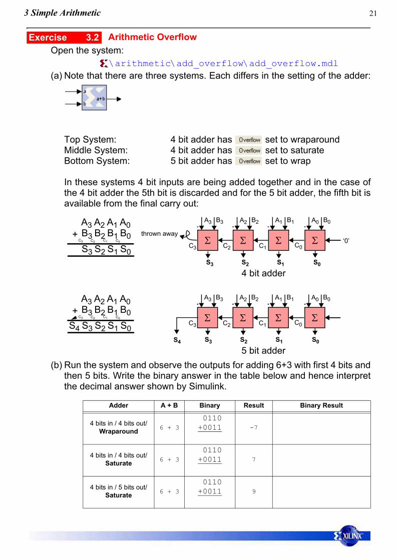
\arithmetic\add_overflow\add_overflow.mdl(a) Note that there are three systems. Each differs in the setting of the adder:
Top System: 4 bit adder has set to wraparoundMiddle System: 4 bit adder has set to saturateBottom System: 5 bit adder has set to wrap
In these systems 4 bit inputs are being added together and in the case ofthe 4 bit adder the 5th bit is discarded and for the 5 bit adder, the fifth bit isavailable from the final carry out:
(b) Run the system and observe the outputs for adding 6+3 with first 4 bits andthen 5 bits. Write the binary answer in the table below and hence interpretthe decimal answer shown by Simulink.
Adder A + B Binary Result Binary Result
4 bits in / 4 bits out/Wraparound 6 + 3
0110 +0011 -7
4 bits in / 4 bits out/Saturate 6 + 3
0110+0011 7
4 bits in / 5 bits out/Saturate 6 + 3
0110+0011 9
Exercise 3.2
Σ
A3 B3
S3
Σ
A2 B2
S2
Σ
A1 B1
S1
Σ
A0 B0
S0
‘0’C0C1C2C3
4 bit adder
Σ
A3 B3
S3
Σ
A2 B2
S2
Σ
A1 B1
S1
Σ
A0 B0
S0
C0C1C2C3
5 bit adderS4
thrown away
A3 A2 A1 A0B3 B2 B1 B0
S4 S3 S2 S1 S0
C3 C2 C1 C0
+
A3 A2 A1 A0B3 B2 B1 B0
S3 S2 S1 S0
C3 C2 C1 C0
+
22
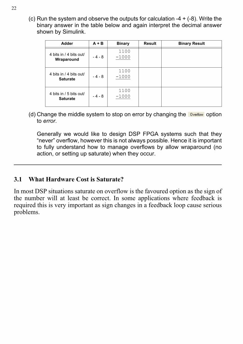
(c) Run the system and observe the outputs for calculation -4 + (-8). Write thebinary answer in the table below and again interpret the decimal answershown by Simulink.
(d) Change the middle system to stop on error by changing the optionto error.
Generally we would like to design DSP FPGA systems such that they“never” overflow, however this is not always possible. Hence it is importantto fully understand how to manage overflows by allow wraparound (noaction, or setting up saturate) when they occur.
3.1 What Hardware Cost is Saturate?
In most DSP situations saturate on overflow is the favoured option as the sign ofthe number will at least be correct. In some applications where feedback isrequired this is very important as sign changes in a feedback loop cause seriousproblems.
Adder A + B Binary Result Binary Result
4 bits in / 4 bits out/Wraparound - 4 - 8
1100 -1000
4 bits in / 4 bits out/Saturate - 4 - 8
1100 -1000
4 bits in / 5 bits out/Saturate - 4 - 8
1100 -1000
233 Simple Arithmetic
Saturation does not come for free however!
Once overflow has been detected, based on an overflow output we could use amultiplexor to then switch in the most positive or most negative 4 bit valuedepending on whether the overflow was negative or positive.
Σ
A3 B3
S3
Σ
A2 B2
S2
Σ
A1 B1
S1
Σ
A0 B0
S0
C0C1C2C3
QUESTION 1: For the 4 bit adder (using 2’s complement arithmetic) below, design someadditional circuitry that will detect when the result has overflowed.
Σ
A3 B3
S3
Σ
A2 B2
S2
Σ
A1 B1
S1
Σ
A0 B0
S0
C0C1C2C3
5 bit adder
QUESTION 2: Using your answer to the previous question design a circuit that will allowsaturate (positive or negative) to be implemented on detection of overflow.
24
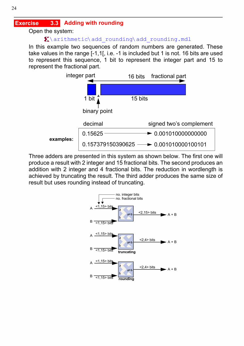
Adding with roundingOpen the system:
\arithmetic\add_rounding\add_rounding.mdlIn this example two sequences of random numbers are generated. Thesetake values in the range [-1,1[, i.e. -1 is included but 1 is not. 16 bits are usedto represent this sequence, 1 bit to represent the integer part and 15 torepresent the fractional part.
Three adders are presented in this system as shown below. The first one willproduce a result with 2 integer and 15 fractional bits. The second produces anaddition with 2 integer and 4 fractional bits. The reduction in wordlength isachieved by truncating the result. The third adder produces the same size ofresult but uses rounding instead of truncating.
Exercise 3.3
15 bits1 bit
binary point
integer part fractional part16 bits
examples:0.15625 0.001010000000000
0.0010100001001010.157379150390625
decimal signed two’s complement
A
B
<1,15> bits
<1,15> bits
<2,15> bits A + B
A
B
<1,15> bits
<1,15> bits
<2,4> bits A + B
A
B
<1,15> bits
<1,15> bits
<2,4> bits A + B
truncating
rounding
no. integer bitsno. fractional bits
253 Simple Arithmetic
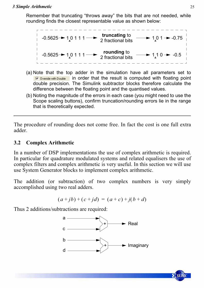
Remember that truncating “throws away” the bits that are not needed, whilerounding finds the closest representable value as shown below:
(a) Note that the top adder in the simulation have all parameters set to in order that the result is computed with floating point
double precision. The Simulink subtractor blocks therefore calculate thedifference between the floating point and the quantised values.
(b) Noting the magnitude of the errors in each case (you might need to use theScope scaling buttons), confirm truncation/rounding errors lie in the rangethat is theoretically expected.
The procedure of rounding does not come free. In fact the cost is one full extraadder.
3.2 Complex Arithmetic
In a number of DSP implementations the use of complex arithmetic is required.In particular for quadrature modulated systems and related equalisers the use ofcomplex filters and complex arithmetic is very useful. In this section we will useuse System Generator blocks to implement complex arithmetic.
The addition (or subtraction) of two complex numbers is very simplyaccomplished using two real adders.
Complex AdditionConfirm the correct operation of the 8 bit adder.
\arithmetic\complex_add\complex_add.mdl
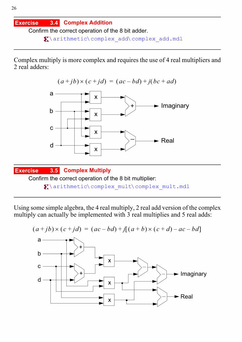
Complex multiply is more complex and requires the use of 4 real multipliers and2 real adders:
Complex MultiplyConfirm the correct operation of the 8 bit multiplier:
\arithmetic\complex_mult\complex_mult.mdl
Using some simple algebra, the 4 real multiply, 2 real add version of the complexmultiply can actually be implemented with 3 real multiplies and 5 real adds:
Exercise 3.4
a jb+( ) c jd+( )× ac bd–( ) j bc ad+( )+=
x+
_Real
Imaginary
a
b
c
d
x
x
x
Exercise 3.5
a jb+( ) c jd+( )× ac bd–( ) j a b+( ) c d+( ) ac– bd–×[ ]+=
+
+
a
b
c
d
_
_
_
Imaginary
Real
x
x
x
274 Designing for Xilinx ISE Tools
4 Designing for Xilinx ISE Tools
In this section we will take some simple designs and from first principlessynthesise them to Xilinx FPGAs. We will start with some very simple exampleswhere we will describe each step and facility in detail.
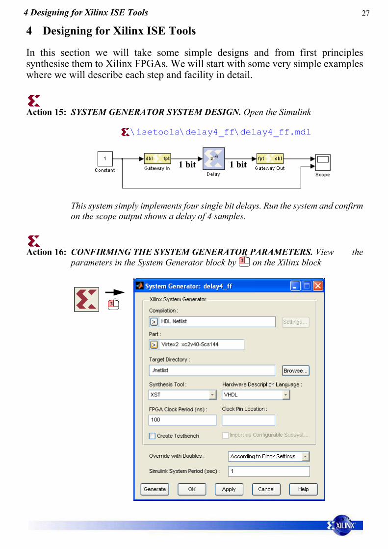
Action 15: SYSTEM GENERATOR SYSTEM DESIGN. Open the Simulink
\isetools\delay4_ff\delay4_ff.mdl
This system simply implements four single bit delays. Run the system and confirmon the scope output shows a delay of 4 samples.
Action 16: CONFIRMING THE SYSTEM GENERATOR PARAMETERS. View theparameters in the System Generator block by on the Xilinx block
1 bit 1 bit
2
2
28
View the various parameters in this window and where necessary check in the on the meanings of the various parameters.
Note that the target device is set to the Virtex2 XC2v40 device.
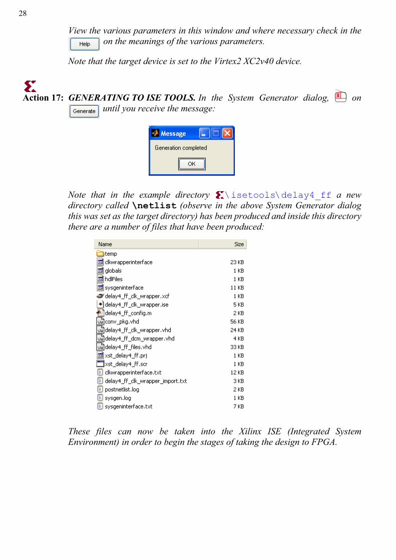
Action 17: GENERATING TO ISE TOOLS. In the System Generator dialog, on until you receive the message:
Note that in the example directory \isetools\delay4_ff a newdirectory called \netlist (observe in the above System Generator dialogthis was set as the target directory) has been produced and inside this directorythere are a number of files that have been produced:
These files can now be taken into the Xilinx ISE (Integrated SystemEnvironment) in order to begin the stages of taking the design to FPGA.
1
294 Designing for Xilinx ISE Tools
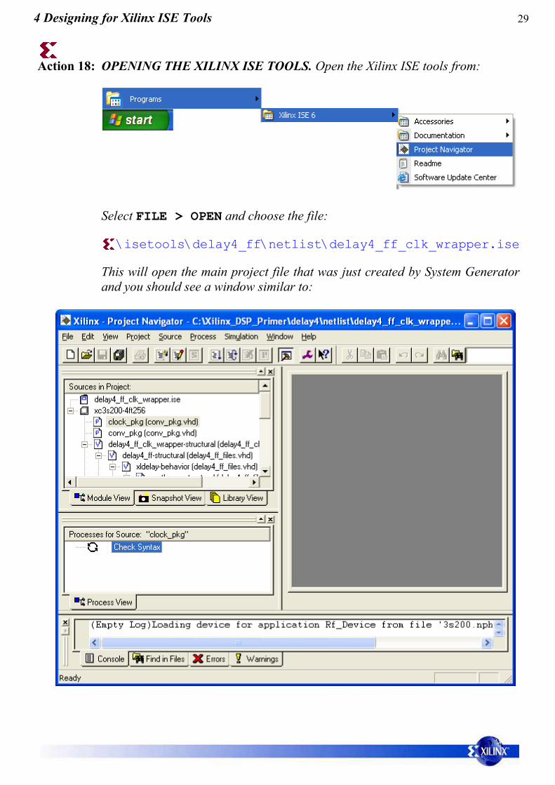
Action 18: OPENING THE XILINX ISE TOOLS. Open the Xilinx ISE tools from:
This will open the main project file that was just created by System Generatorand you should see a window similar to:
30
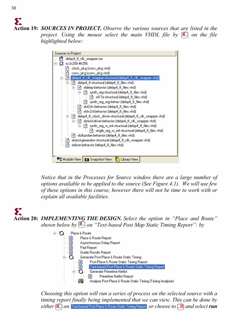
Action 19: SOURCES IN PROJECT. Observe the various sources that are listed in theproject. Using the mouse select the main VHDL file by on the filehighlighted below:
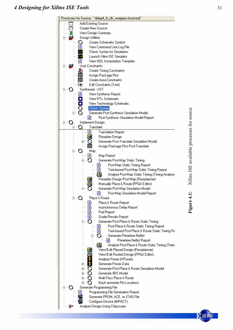
Notice that in the Processes for Source window there are a large number ofoptions available to be applied to the source (See Figure 4.1). We will use fewof these options in this course, however there will not be time to work with orexplain all available facilities.
Action 20: IMPLEMENTING THE DESIGN. Select the option in “Place and Route”shown below by on “Text-based Post Map Static Timing Report”: by
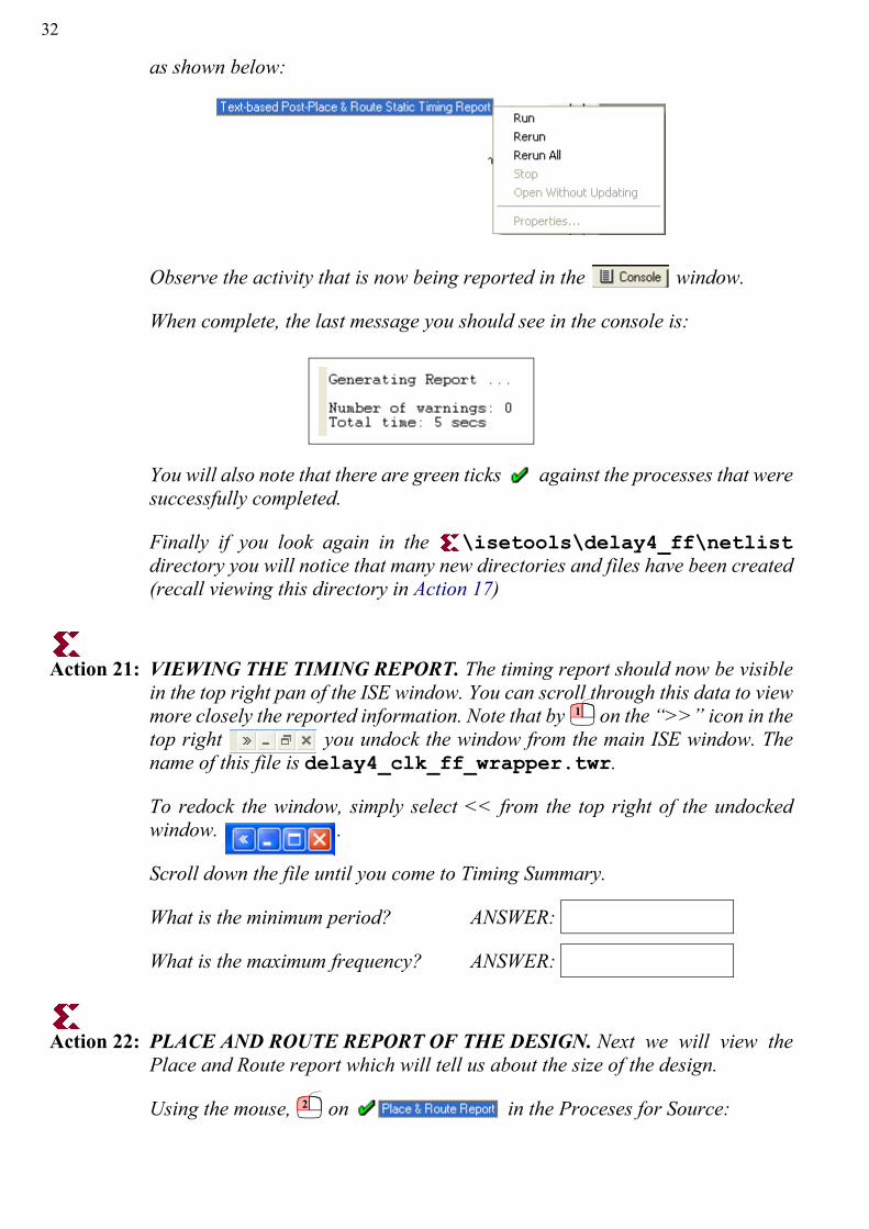
Choosing this option will run a series of process on the selected source with atiming report finally being implemented that we can view. This can be done byeither on or choose to and select run
1
1
2 1
314 Designing for Xilinx ISE Tools
Figu
re 4
.1:
Xili
nx IS
E av
aila
ble
proc
esse
s for
sour
ce
32
as shown below:
Observe the activity that is now being reported in the window.
When complete, the last message you should see in the console is:
You will also note that there are green ticks against the processes that weresuccessfully completed.
Finally if you look again in the \isetools\delay4_ff\netlistdirectory you will notice that many new directories and files have been created(recall viewing this directory in Action 17)
Action 21: VIEWING THE TIMING REPORT. The timing report should now be visiblein the top right pan of the ISE window. You can scroll through this data to viewmore closely the reported information. Note that by on the “>>” icon in thetop right you undock the window from the main ISE window. Thename of this file is delay4_clk_ff_wrapper.twr.
To redock the window, simply select << from the top right of the undockedwindow. .
Scroll down the file until you come to Timing Summary.
What is the minimum period? ANSWER:
What is the maximum frequency? ANSWER:
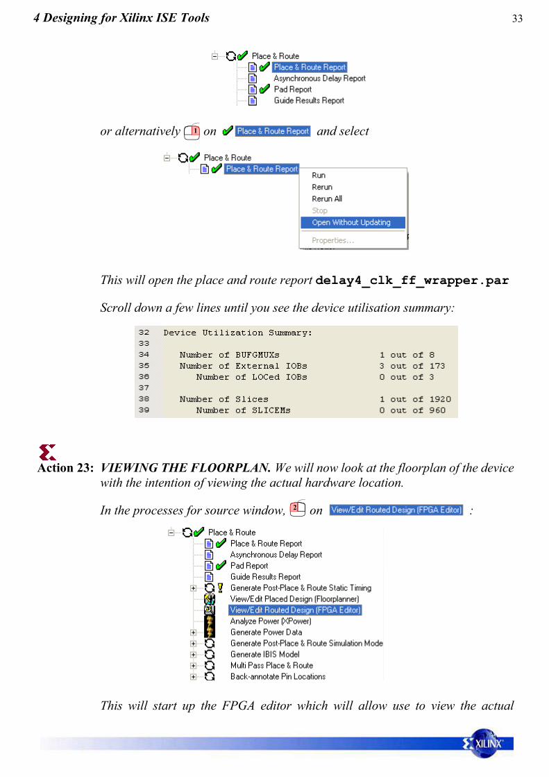
Action 22: PLACE AND ROUTE REPORT OF THE DESIGN. Next we will view thePlace and Route report which will tell us about the size of the design.
Using the mouse, on in the Proceses for Source:
1
2
334 Designing for Xilinx ISE Tools
or alternatively on and select
This will open the place and route report delay4_clk_ff_wrapper.par
Scroll down a few lines until you see the device utilisation summary:
Action 23: VIEWING THE FLOORPLAN. We will now look at the floorplan of the devicewith the intention of viewing the actual hardware location.
In the processes for source window, on :
This will start up the FPGA editor which will allow use to view the actual
1
2
34
implementation and inspect various slices and interconnections.
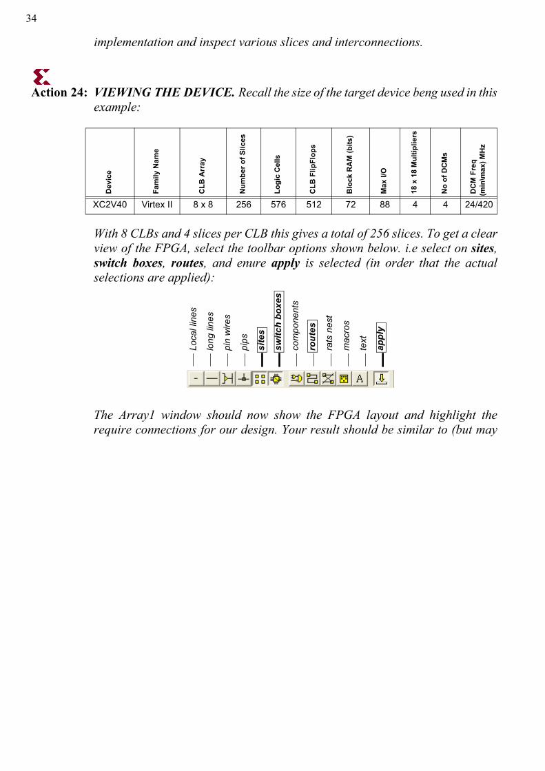
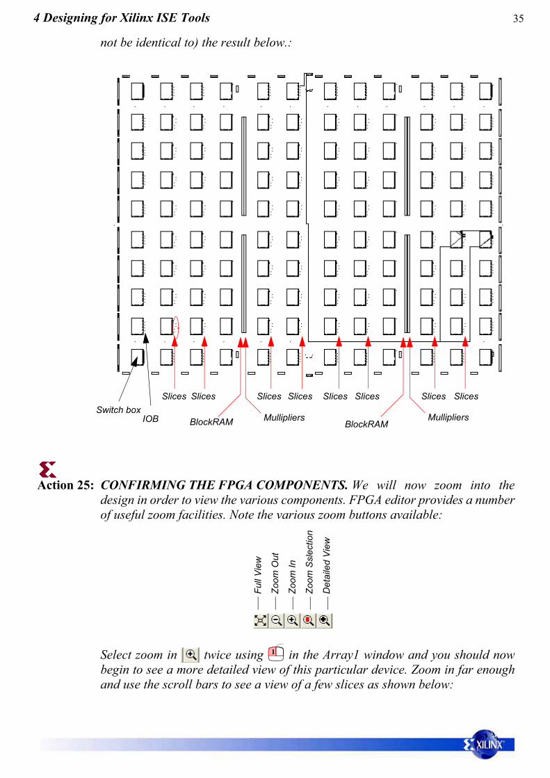
Action 24: VIEWING THE DEVICE. Recall the size of the target device beng used in thisexample:
With 8 CLBs and 4 slices per CLB this gives a total of 256 slices. To get a clearview of the FPGA, select the toolbar options shown below. i.e select on sites,switch boxes, routes, and enure apply is selected (in order that the actualselections are applied):
The Array1 window should now show the FPGA layout and highlight therequire connections for our design. Your result should be similar to (but may
Dev
ice
Fam
ily N
ame
CLB
Arr
ay
Num
ber o
f Slic
es
Logi
c C
ells
CLB
Flip
Flop
s
Blo
ck R
AM
(bits
)
Max
I/O
18 x
18
Mul
tiplie
rs
No
of D
CM
s
DC
M F
req
(min
\max
) MH
z
XC2V40 Virtex II 8 x 8 256 576 512 72 88 4 4 24/420Lo
cal l
ines
long
line
s
pin
wire
s
pips
site
s
switc
h bo
xes
com
pone
nts
rout
es
rats
nes
t
mac
ros
text
appl
y
354 Designing for Xilinx ISE Tools
not be identical to) the result below.:
Action 25: CONFIRMING THE FPGA COMPONENTS. We will now zoom into thedesign in order to view the various components. FPGA editor provides a numberof useful zoom facilities. Note the various zoom buttons available:
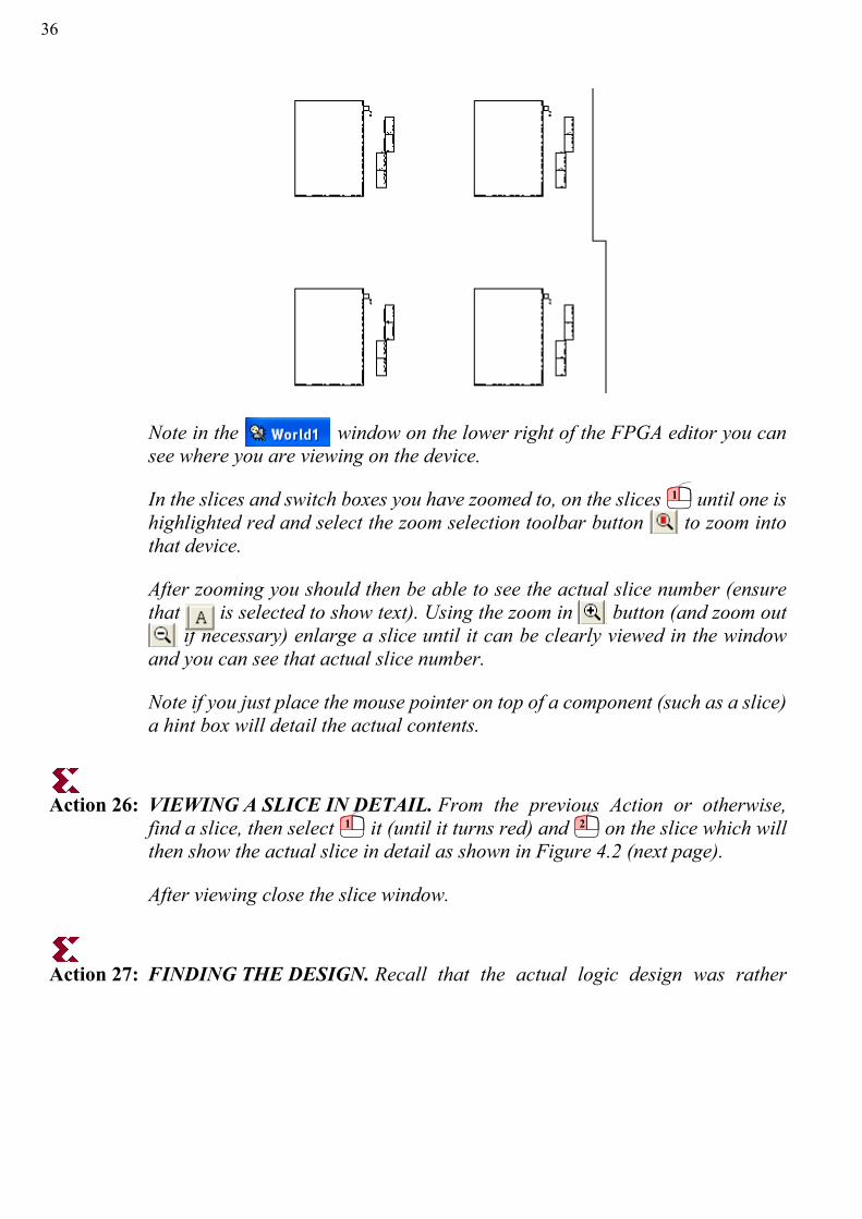
Select zoom in twice using in the Array1 window and you should nowbegin to see a more detailed view of this particular device. Zoom in far enoughand use the scroll bars to see a view of a few slices as shown below:
Note in the window on the lower right of the FPGA editor you cansee where you are viewing on the device.
In the slices and switch boxes you have zoomed to, on the slices until one ishighlighted red and select the zoom selection toolbar button to zoom intothat device.
After zooming you should then be able to see the actual slice number (ensurethat is selected to show text). Using the zoom in button (and zoom out
if necessary) enlarge a slice until it can be clearly viewed in the windowand you can see that actual slice number.
Note if you just place the mouse pointer on top of a component (such as a slice)a hint box will detail the actual contents.
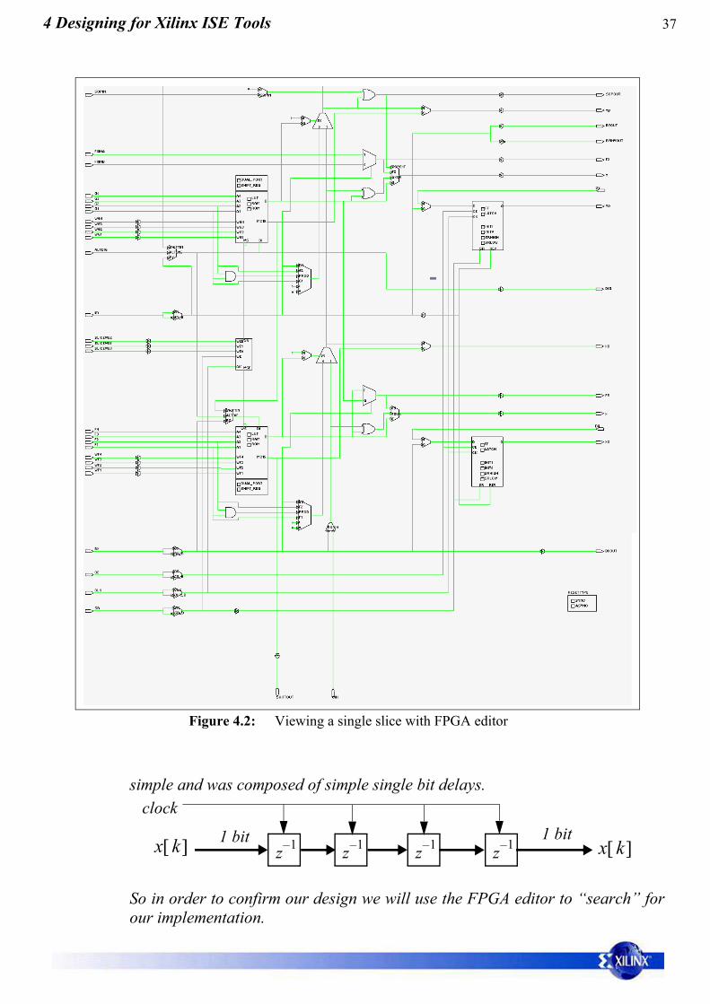
Action 26: VIEWING A SLICE IN DETAIL. From the previous Action or otherwise,find a slice, then select it (until it turns red) and on the slice which willthen show the actual slice in detail as shown in Figure 4.2 (next page).
After viewing close the slice window.
Action 27: FINDING THE DESIGN. Recall that the actual logic design was rather
1
1 2
374 Designing for Xilinx ISE Tools
simple and was composed of simple single bit delays.
So in order to confirm our design we will use the FPGA editor to “search” forour implementation.
Figure 4.2: Viewing a single slice with FPGA editor
z 1– z 1– z 1–x k[ ] x k[ ]
clock1 bit1 bit
z 1–
38
Choose to zoom out to a full screen view by on . Ensure that thefollowing toolbar options are set:
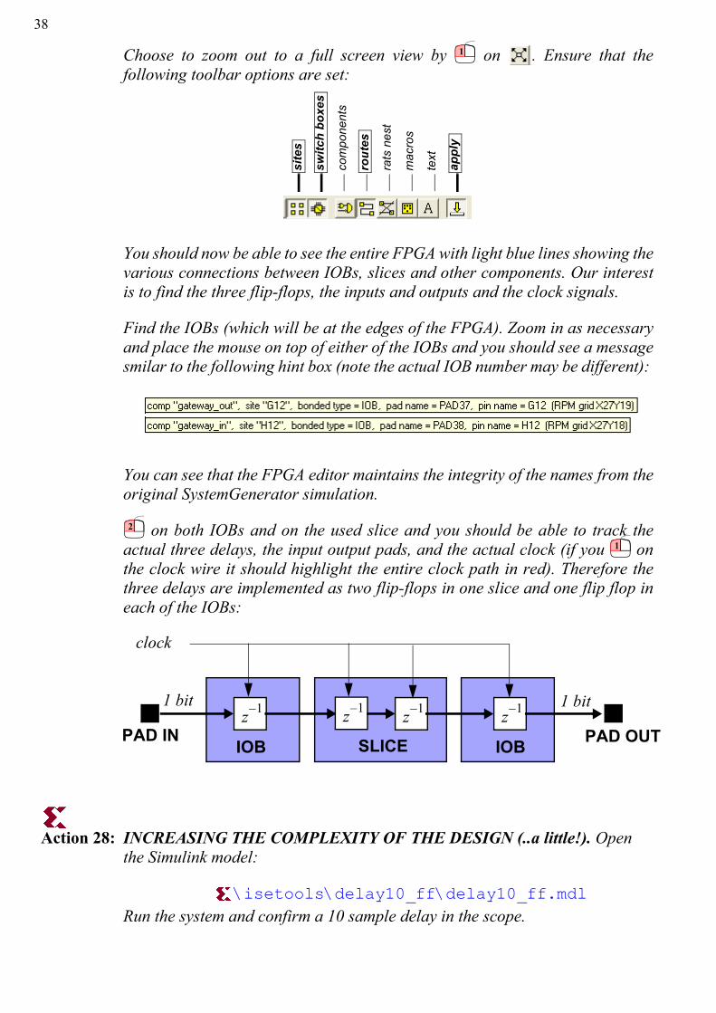
You should now be able to see the entire FPGA with light blue lines showing thevarious connections between IOBs, slices and other components. Our interestis to find the three flip-flops, the inputs and outputs and the clock signals.
Find the IOBs (which will be at the edges of the FPGA). Zoom in as necessaryand place the mouse on top of either of the IOBs and you should see a messagesmilar to the following hint box (note the actual IOB number may be different):
You can see that the FPGA editor maintains the integrity of the names from theoriginal SystemGenerator simulation.
on both IOBs and on the used slice and you should be able to track theactual three delays, the input output pads, and the actual clock (if you onthe clock wire it should highlight the entire clock path in red). Therefore thethree delays are implemented as two flip-flops in one slice and one flip flop ineach of the IOBs:
Action 28: INCREASING THE COMPLEXITY OF THE DESIGN (..a little!). Openthe Simulink model:
\isetools\delay10_ff\delay10_ff.mdlRun the system and confirm a 10 sample delay in the scope.
1
site
s
switc
h bo
xes
com
pone
nts
rout
es
rats
nes
t
mac
ros
text
appl
y
2
1
z 1– z 1– z 1–
clock
1 bit
IOB IOBSLICE
1 bit
PAD IN PAD OUTz 1–
394 Designing for Xilinx ISE Tools
in the System Generator block and then in the System Generator dialog, on . The new ISE project will now be produced.
Go to the Xilinx ISE tools again and select FILE > OPEN and choose the file:
Repeat Action 19 (page 32) to Action 22 in order to produce the Timing Reportand the Place and Route report and complete the table below:
You should notice that the speed has dropped slighlty, and the number of sliceshas increased by a factor 4. Can you justify this compared to the previous designwith only 3 delays?
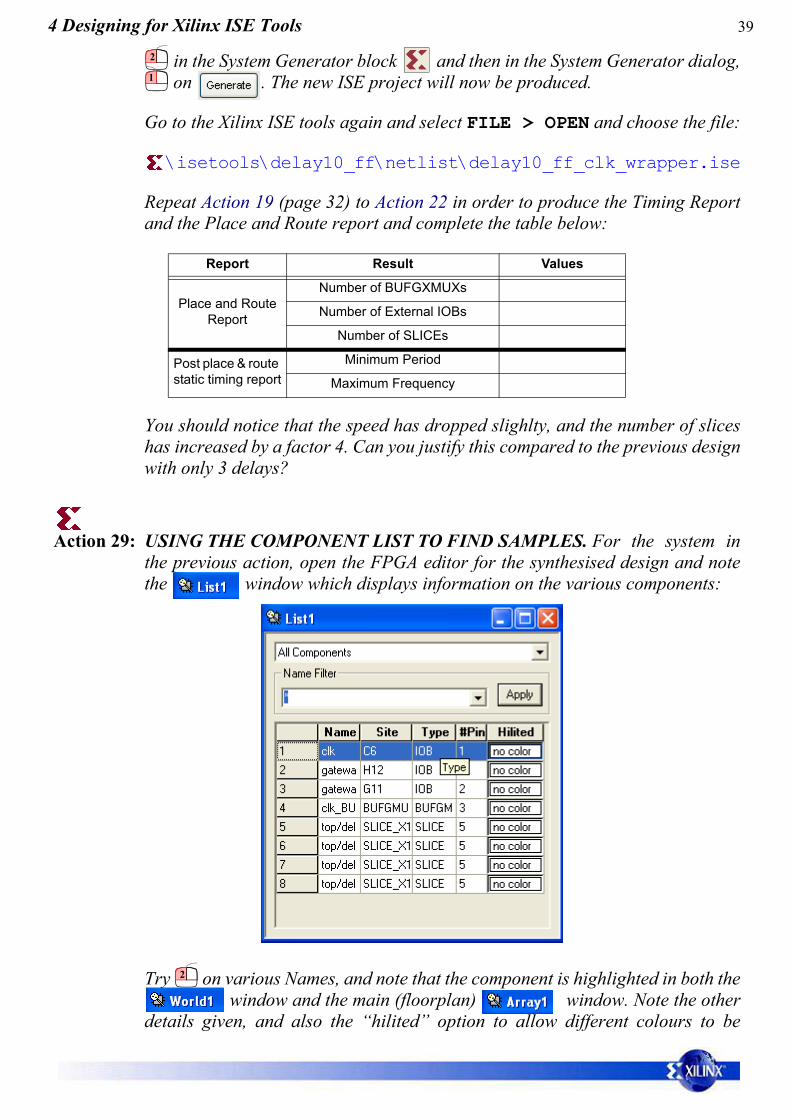
Action 29: USING THE COMPONENT LIST TO FIND SAMPLES. For the system inthe previous action, open the FPGA editor for the synthesised design and notethe window which displays information on the various components:
Try on various Names, and note that the component is highlighted in both the window and the main (floorplan) window. Note the other
details given, and also the “hilited” option to allow different colours to be
Report Result Values
Place and Route Report
Number of BUFGXMUXs
Number of External IOBs
Number of SLICEs
Post place & route static timing report
Minimum Period
Maximum Frequency
2
1
2
40
assigned to different components.
Search through the floorplan to find the 8 single delays.
4.1 Building Delays Lines
In this section (now that we have used the various Simulink, System Generatorand Xilinx ISE tools) we will produce delays lines and select a few options fromin doing this.
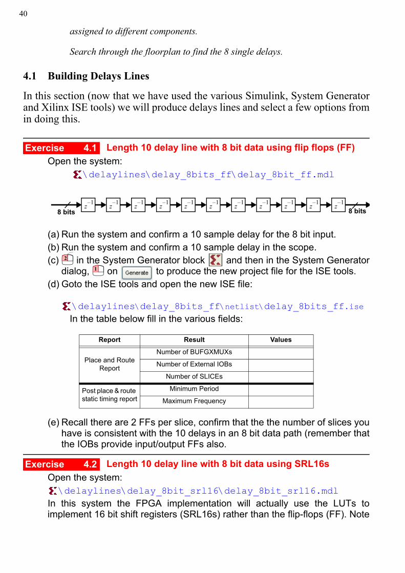
Length 10 delay line with 8 bit data using flip flops (FF)Open the system:
\delaylines\delay_8bits_ff\delay_8bit_ff.mdl
(a) Run the system and confirm a 10 sample delay for the 8 bit input. (b) Run the system and confirm a 10 sample delay in the scope.(c) in the System Generator block and then in the System Generator
dialog, on to produce the new project file for the ISE tools.(d) Goto the ISE tools and open the new ISE file:
\delaylines\delay_8bits_ff\netlist\delay_8bits_ff.iseIn the table below fill in the various fields:
(e) Recall there are 2 FFs per slice, confirm that the the number of slices youhave is consistent with the 10 delays in an 8 bit data path (remember thatthe IOBs provide input/output FFs also.
Length 10 delay line with 8 bit data using SRL16sOpen the system:\delaylines\delay_8bit_srl16\delay_8bit_srl16.mdl
In this system the FPGA implementation will actually use the LUTs toimplement 16 bit shift registers (SRL16s) rather than the flip-flops (FF). Note
Report Result Values
Place and Route Report
Number of BUFGXMUXs
Number of External IOBs
Number of SLICEs
Post place & route static timing report
Minimum Period
Maximum Frequency
Exercise 4.1
z 1–z 1– z 1– z 1– z 1– z 1– z 1– z 1– z 1– z 1– z 1–
8 bits 8 bits
2
1
Exercise 4.2
414 Designing for Xilinx ISE Tools
that this is something that can be explicitly setup in the actual delay block.
(a) on the delay block and note the text at the top:
“Hardware notes: A delay line is a chain, each link of which is an SRL16followed by a flip-flop. If register timing is enabled, the delay line is a chainof flip-flops.”
In the previous Exercise 4.1, register timing was enabled and hence thefinal implementation used a chain of flip-flops.
(b) Run the Simulink system and then following the same procedures aspreviously, take the system all the way to the ISE tools and complete thetable below:
(c) Compare this to the previous result from Exercise 4.1. (d) View the actual FPGA implementation and observe the use of the LUTs as
shift registers (SRL16). (e) Given the total number of slices used, confirm this is about the number you
would expect for this 8 bit, 10 sample delay line.
4.2 Arithmetic Components
In this section we will produce a few simple implementations of the arithmeticoperations of addition and multiplication in order to see how this is implementedin slice logic.
Report Result Values
Place and Route Report
Number of BUFGXMUXs
Number of External IOBs
Number of SLICEs
Post place & route static timing report
Minimum Period
Maximum Frequency
2
42
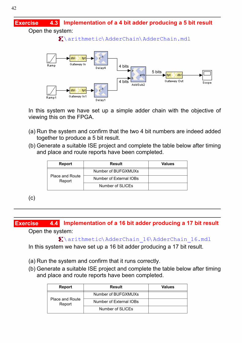
Implementation of a 4 bit adder producing a 5 bit resultOpen the system:
\arithmetic\AdderChain\AdderChain.mdl
In this system we have set up a simple adder chain with the objective ofviewing this on the FPGA.
(a) Run the system and confirm that the two 4 bit numbers are indeed addedtogether to produce a 5 bit result.
(b) Generate a suitable ISE project and complete the table below after timingand place and route reports have been completed.
(c)
Implementation of a 16 bit adder producing a 17 bit resultOpen the system:
\arithmetic\AdderChain_16\AdderChain_16.mdl In this system we have set up a 16 bit adder producing a 17 bit result.
(a) Run the system and confirm that it runs correctly.(b) Generate a suitable ISE project and complete the table below after timing
and place and route reports have been completed.
Report Result Values
Place and Route Report
Number of BUFGXMUXs
Number of External IOBs
Number of SLICEs
Report Result Values
Place and Route Report
Number of BUFGXMUXs
Number of External IOBs
Number of SLICEs
Exercise 4.3
4 bits
4 bits
5 bits
Exercise 4.4
435 FIR filtering
(c) How does this compare to the previous exercise?
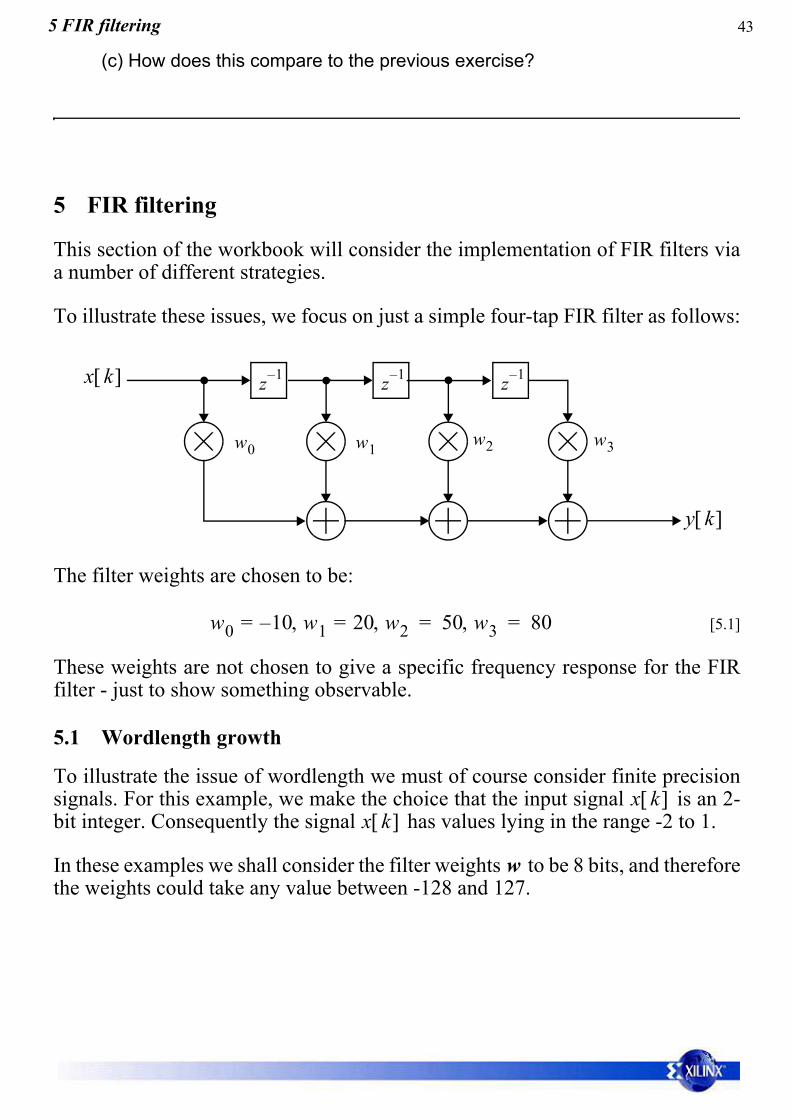
5 FIR filtering
This section of the workbook will consider the implementation of FIR filters viaa number of different strategies.
To illustrate these issues, we focus on just a simple four-tap FIR filter as follows:
The filter weights are chosen to be:
[5.1]
These weights are not chosen to give a specific frequency response for the FIRfilter - just to show something observable.
5.1 Wordlength growth
To illustrate the issue of wordlength we must of course consider finite precisionsignals. For this example, we make the choice that the input signal is an 2-bit integer. Consequently the signal has values lying in the range -2 to 1.
In these examples we shall consider the filter weights to be 8 bits, and thereforethe weights could take any value between -128 and 127.
z 1– z 1– z 1–x k[ ]
w0 w1 w2 w3
y k[ ]
w0 10– w1, 20= = w2, 50 w3, 80= =
x k[ ]x k[ ]
w
44
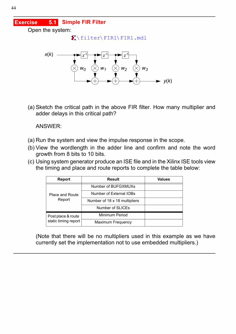
Simple FIR FilterOpen the system:
\filter\FIR1\FIR1.mdl
(a) Sketch the critical path in the above FIR filter. How many multiplier andadder delays in this critical path?
ANSWER:
(a) Run the system and view the impulse response in the scope.(b) View the wordlength in the adder line and confirm and note the word
growth from 8 bits to 10 bits.(c) Using system generator produce an ISE file and in the Xilinx ISE tools view
the timing and place and route reports to complete the table below:
(Note that there will be no multipliers used in this example as we havecurrently set the implementation not to use embedded multipliers.)
Report Result Values
Place and Route Report
Number of BUFGXMUXs
Number of External IOBs
Number of 18 x 18 multipliers
Number of SLICEs
Post place & route static timing report
Minimum Period
Maximum Frequency
Exercise 5.1
w0 w1 w2 w3
y(k)
x(k) z-1z-1z-1
455 FIR filtering
Retiming FIR FilterOpen the system:
\filter\FIR2\FIR2.mdl
This system has been produced by applying the cut sets in the top figure toproduce the signal flow graph in the lower figure in order to reduce the criticalpath latency.(a) Run the system and view the impulse response in the scope.
Note that compared to the previous example the critical path latency is nowmuch shorter. What is the new critical path latency?
ANSWER:
Exercise 5.2
w0 w1 w2 w3
z(k) = y(k-4)
x(k) z-2z-2z-2
z-1z-1z-1
w0 w1 w2 w3
y(k)
x(k) z-1z-1z-1
cut sets
46
(b) Using system generator produce an ISE file and in the Xilinx ISE tools viewthe timing and place and route reports to complete the table below: :
This should run faster than the previous example due to the shorter criticalpath, but will require some more hardware.
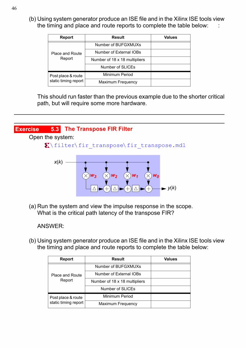
The Transpose FIR FilterOpen the system:
\filter\fir_transpose\fir_transpose.mdl
(a) Run the system and view the impulse response in the scope.What is the critical path latency of the transpose FIR?
ANSWER:
(b) Using system generator produce an ISE file and in the Xilinx ISE tools viewthe timing and place and route reports to complete the table below:
Report Result Values
Place and Route Report
Number of BUFGXMUXs
Number of External IOBs
Number of 18 x 18 multipliers
Number of SLICEs
Post place & route static timing report
Minimum Period
Maximum Frequency
Report Result Values
Place and Route Report
Number of BUFGXMUXs
Number of External IOBs
Number of 18 x 18 multipliers
Number of SLICEs
Post place & route static timing report
Minimum Period
Maximum Frequency
Exercise 5.3
x(k)
y(k)
w0w1w2w3
475 FIR filtering
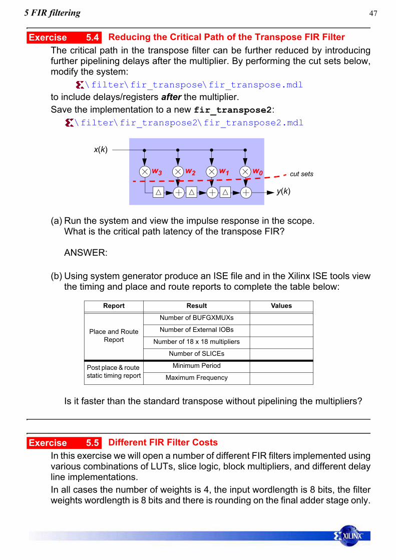
Reducing the Critical Path of the Transpose FIR FilterThe critical path in the transpose filter can be further reduced by introducingfurther pipelining delays after the multiplier. By performing the cut sets below,modify the system:
\filter\fir_transpose\fir_transpose.mdlto include delays/registers after the multiplier.Save the implementation to a new fir_transpose2:
\filter\fir_transpose2\fir_transpose2.mdl
(a) Run the system and view the impulse response in the scope.What is the critical path latency of the transpose FIR?
ANSWER:
(b) Using system generator produce an ISE file and in the Xilinx ISE tools viewthe timing and place and route reports to complete the table below:
Is it faster than the standard transpose without pipelining the multipliers?
Different FIR Filter CostsIn this exercise we will open a number of different FIR filters implemented usingvarious combinations of LUTs, slice logic, block multipliers, and different delayline implementations.In all cases the number of weights is 4, the input wordlength is 8 bits, the filterweights wordlength is 8 bits and there is rounding on the final adder stage only.
Report Result Values
Place and Route Report
Number of BUFGXMUXs
Number of External IOBs
Number of 18 x 18 multipliers
Number of SLICEs
Post place & route static timing report
Minimum Period
Maximum Frequency
Exercise 5.4
x(k)
y(k)
w0w1w2w3 cut sets
Exercise 5.5
48
Run them in Simulink then compare the timings and hardware costs from theplace and route reports and the timing reports.
(i) FIR Filter Using SRL16s Delay Lines\filter\fir_srl16\fir_srl16.mdl :
(ii) FIR Filter Using FF Delay Lines\filter\fir_ff\fir_ff.mdl :
(iii) FIR Filter Using Distributed Arithmetic Core\filter\fir_ff_da\fir_ff_da.mdl :
Report Result Values
Place and Route Report
Number of BUFGXMUXs
Number of External IOBs
Number of 18 x 18 multipliers
Number of SLICEs
Post place & route static timing report
Minimum Period
Maximum Frequency
Report Result Values
Place and Route Report
Number of BUFGXMUXs
Number of External IOBs
Number of 18 x 18 multipliers
Number of SLICEs
Post place & route static timing report
Minimum Period
Maximum Frequency
Report Result Values
Place and Route Report
Number of BUFGXMUXs
Number of External IOBs
Number of 18 x 18 multipliers
Number of SLICEs
Post place & route static timing report
Minimum Period
Maximum Frequency
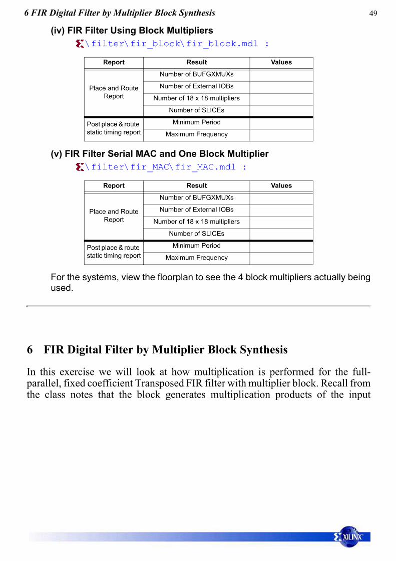
496 FIR Digital Filter by Multiplier Block Synthesis
(iv) FIR Filter Using Block Multipliers \filter\fir_block\fir_block.mdl :
(v) FIR Filter Serial MAC and One Block Multiplier\filter\fir_MAC\fir_MAC.mdl :
For the systems, view the floorplan to see the 4 block multipliers actually beingused.
6 FIR Digital Filter by Multiplier Block Synthesis
In this exercise we will look at how multiplication is performed for the full-parallel, fixed coefficient Transposed FIR filter with multiplier block. Recall fromthe class notes that the block generates multiplication products of the input
Report Result Values
Place and Route Report
Number of BUFGXMUXs
Number of External IOBs
Number of 18 x 18 multipliers
Number of SLICEs
Post place & route static timing report
Minimum Period
Maximum Frequency
Report Result Values
Place and Route Report
Number of BUFGXMUXs
Number of External IOBs
Number of 18 x 18 multipliers
Number of SLICEs
Post place & route static timing report
Minimum Period
Maximum Frequency
50
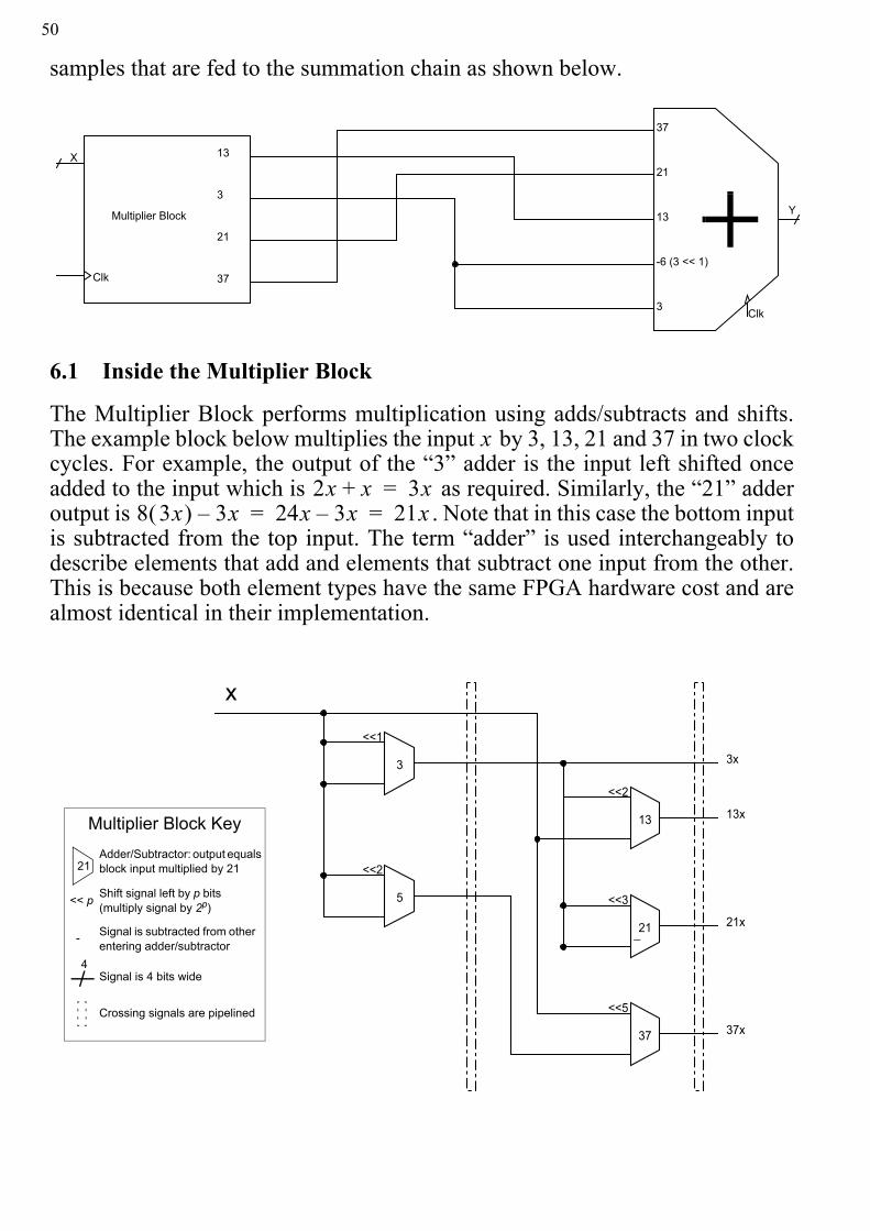
samples that are fed to the summation chain as shown below.
6.1 Inside the Multiplier Block
The Multiplier Block performs multiplication using adds/subtracts and shifts.The example block below multiplies the input by 3, 13, 21 and 37 in two clockcycles. For example, the output of the “3” adder is the input left shifted onceadded to the input which is as required. Similarly, the “21” adderoutput is . Note that in this case the bottom inputis subtracted from the top input. The term “adder” is used interchangeably todescribe elements that add and elements that subtract one input from the other.This is because both element types have the same FPGA hardware cost and arealmost identical in their implementation.
Y
Clk
37
21
13
-6 (3 << 1)
3
Multiplier Block
X
Clk
13
3
21
37
x
2x x+ 3x=8 3x( ) 3x– 24x 3x– 21x= =
3x
37x
13x
21x
37
<<5
13
<<2
21
<<3
_
5
<<2
3
<<1
<< p Shift signal left by p bits (multiply signal by 2p)
- Signal is subtracted from other entering adder/subtractor
Adder/Subtractor: output equals block input multiplied by 2121
Crossing signals are pipelined
Multiplier Block Key
4Signal is 4 bits wide
x
516 FIR Digital Filter by Multiplier Block Synthesis
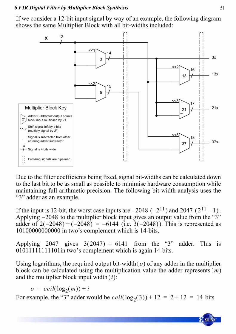
If we consider a 12-bit input signal by way of an example, the following diagramshows the same Multiplier Block with all bit-widths included:
Due to the filter coefficients being fixed, signal bit-widths can be calculated downto the last bit to be as small as possible to minimise hardware consumption whilemaintaining full arithmetic precision. The following bit-width analysis uses the“3” adder as an example.
If the input is 12-bit, the worst case inputs are ( ) and .Applying to the multiplier block input gives an output value from the “3”adder of (i.e. ). This is represented as10100000000000 in two’s complement which is 14-bits.
Applying gives from the “3” adder. This is01011111111101in two’s complement which is again 14-bits.
Using logarithms, the required output bit-width of any adder in the multiplierblock can be calculated using the multiplication value the adder represents and the multiplier block input width :
For example, the “3” adder would be bits
3x
37x
13x
21x
1837
<<5
1613
<<2
1721
<<3
_
155
<<2
143
<<1
12
<< p Shift signal left by p bits (multiply signal by 2p)
- Signal is subtracted from other entering adder/subtractor
Adder/Subtractor: output equals block input multiplied by 2121
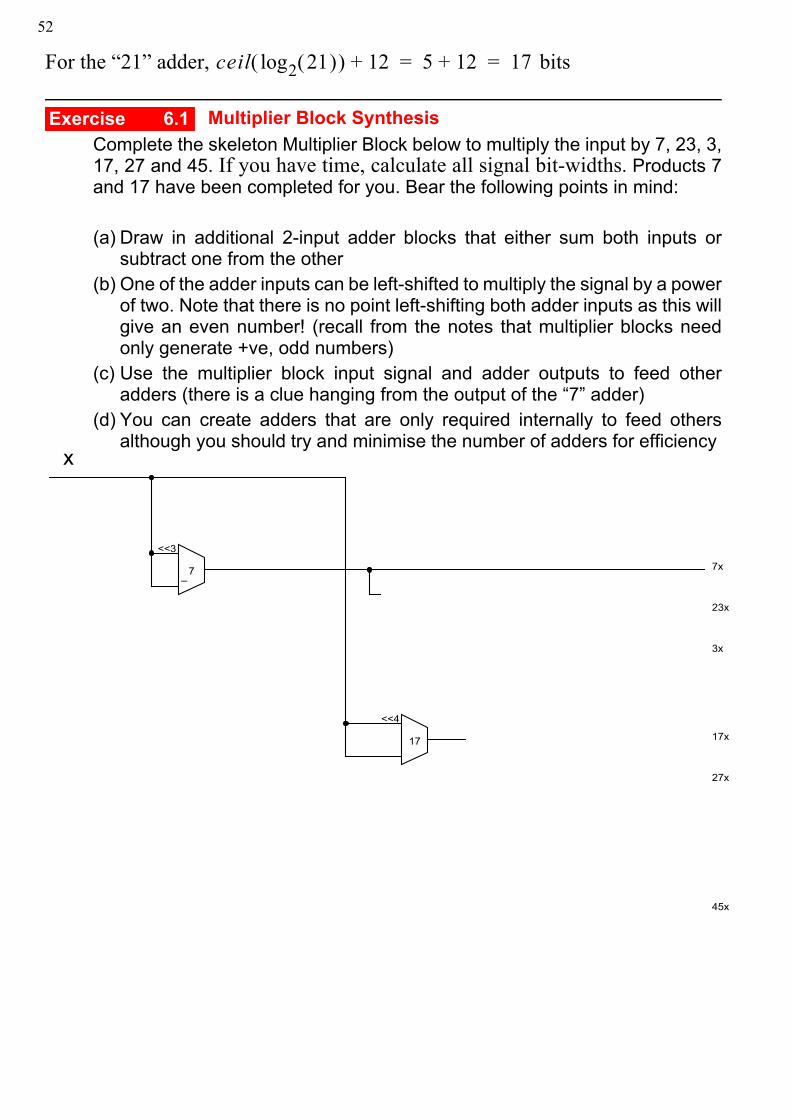
Multiplier Block SynthesisComplete the skeleton Multiplier Block below to multiply the input by 7, 23, 3,17, 27 and 45. If you have time, calculate all signal bit-widths. Products 7and 17 have been completed for you. Bear the following points in mind:
(a) Draw in additional 2-input adder blocks that either sum both inputs orsubtract one from the other
(b) One of the adder inputs can be left-shifted to multiply the signal by a powerof two. Note that there is no point left-shifting both adder inputs as this willgive an even number! (recall from the notes that multiplier blocks needonly generate +ve, odd numbers)
(c) Use the multiplier block input signal and adder outputs to feed otheradders (there is a clue hanging from the output of the “7” adder)
(d) You can create adders that are only required internally to feed othersalthough you should try and minimise the number of adders for efficiency
ceil log2 21( )( ) 12+ 5 12+ 17= =
Exercise 6.1
7x
23x
17x
45x
27x
3x
17
<<4
7
<<3
_
x
537 Adaptive Filtering
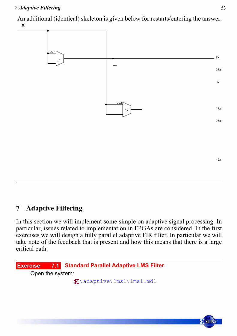
An additional (identical) skeleton is given below for restarts/entering the answer.
7 Adaptive Filtering
In this section we will implement some simple on adaptive signal processing. Inparticular, issues related to implementation in FPGAs are considered. In the firstexercises we will design a fully parallel adaptive FIR filter. In particular we willtake note of the feedback that is present and how this means that there is a largecritical path.
Standard Parallel Adaptive LMS FilterOpen the system:
\adaptive\lms1\lms1.mdl
7x
23x
17x
45x
27x
3x
17
<<4
7
<<3
_
x
Exercise 7.1
54
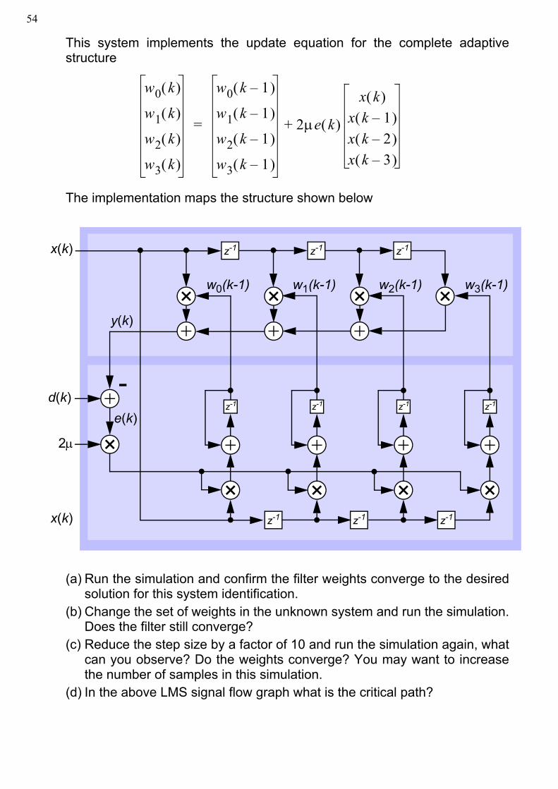
This system implements the update equation for the complete adaptivestructure
The implementation maps the structure shown below
(a) Run the simulation and confirm the filter weights converge to the desiredsolution for this system identification.
(b) Change the set of weights in the unknown system and run the simulation.Does the filter still converge?
(c) Reduce the step size by a factor of 10 and run the simulation again, whatcan you observe? Do the weights converge? You may want to increasethe number of samples in this simulation.
(d) In the above LMS signal flow graph what is the critical path?
w0 k( )
w1 k( )
w2 k( )
w3 k( )
w0 k 1–( )
w1 k 1–( )
w2 k 1–( )
w3 k 1–( )
2µe k( )
x k( )x k 1–( )x k 2–( )x k 3–( )
+=
z-1 z-1 z-1 z-1
z-1 z-1z-1
z-1z-1z-1
w0(k-1)
x(k)
y(k)
d(k)-
2µ
w1(k-1) w2(k-1) w3(k-1)
e(k)
x(k)
557 Adaptive Filtering
(e) Using System Generator and again targetting the XC2V40 with its 4multipliers, synthesise this to an FPGA design using the usual procedure tothe ISE tools.
(f) If you synthesized successfully, complete the table below.
(g) Save the Simulink file to a new directory lms2, and filename of lms2.mdl.Use the System Generator tools again, but this time target the larger device,the XCVP30 from the VIrtex II Pro family (and available on the board usedin this course). Again, complete the table below:
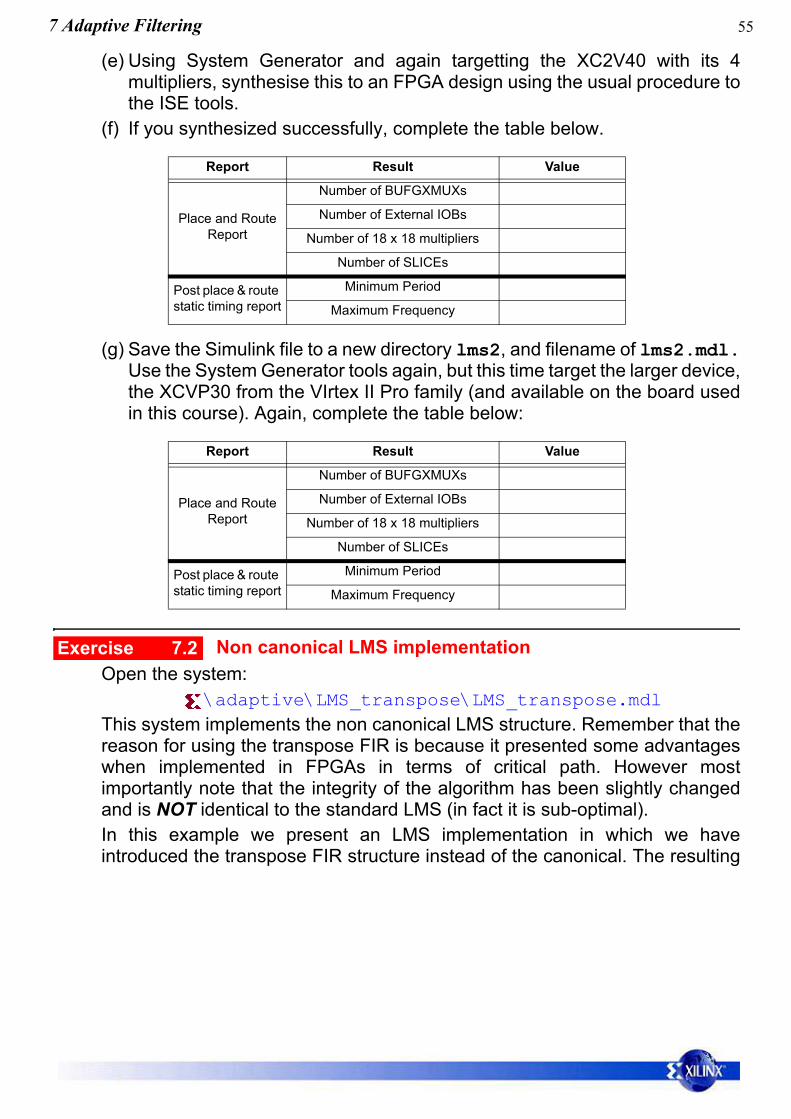
Non canonical LMS implementationOpen the system:
\adaptive\LMS_transpose\LMS_transpose.mdlThis system implements the non canonical LMS structure. Remember that thereason for using the transpose FIR is because it presented some advantageswhen implemented in FPGAs in terms of critical path. However mostimportantly note that the integrity of the algorithm has been slightly changedand is NOT identical to the standard LMS (in fact it is sub-optimal).In this example we present an LMS implementation in which we haveintroduced the transpose FIR structure instead of the canonical. The resulting
Report Result Value
Place and Route Report
Number of BUFGXMUXs
Number of External IOBs
Number of 18 x 18 multipliers
Number of SLICEs
Post place & route static timing report
Minimum Period
Maximum Frequency
Report Result Value
Place and Route Report
Number of BUFGXMUXs
Number of External IOBs
Number of 18 x 18 multipliers
Number of SLICEs
Post place & route static timing report
Minimum Period
Maximum Frequency
Exercise 7.2
56
implementation of the LMS is called the non-canonical LMS and is shown inthe figure below.
(a) Check the configuration in the provided System Generator file and confirmit implements the structure shown above.
(b) Run the simulation and confirm the filter weights converge to the desiredsolution.
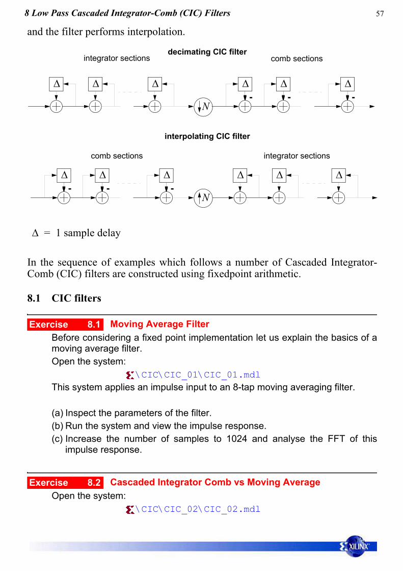
8 Low Pass Cascaded Integrator-Comb (CIC) Filters
Cascaded integrator-comb filters provide an efficient way to perform resamplingin a multi-rate DSP system. As suggested by the name, these filters areconstructed using integrators and comb filters. The diagram below shows thetwo most common CIC filter configurations. In the first configuration theintegrator sections preceed the comb sections and the filter performs decimation.In the second configuration the comb sections preceed the integrator sections
In the sequence of examples which follows a number of Cascaded Integrator-Comb (CIC) filters are constructed using fixedpoint arithmetic.
8.1 CIC filters
Moving Average FilterBefore considering a fixed point implementation let us explain the basics of amoving average filter.Open the system:
\CIC\CIC_01\CIC_01.mdlThis system applies an impulse input to an 8-tap moving averaging filter.
(a) Inspect the parameters of the filter.(b) Run the system and view the impulse response.(c) Increase the number of samples to 1024 and analyse the FFT of this
impulse response.
Cascaded Integrator Comb vs Moving AverageOpen the system:
This example shows how a Cascaded Integrator-Comb filter is equivalent toa non-recursive moving average filter.
(a) Inspect the block parameters, run the system and, observe that the CICfrequency response is equivalent to that of the moving average filter.
(b) Swap the order of the integrator and comb sections. Does the system stillhave the same response?
Multi-Stage CIC FilterOpen the system:
\CIC\CIC_03\CIC_03.mdl
This system consists of three CIC "stages" where each stage consists of anintegrator-comb pair. The impulse response at the output of each stage isanalysed. Note that each CIC stage has a dc gain of 8. For this reasoncompensation gains have been used to normalise the impulse responsemeasurements to have a dc gain of 1 (0dB).
(a) Run the system and view the frequency response.(b) Observe the difference between the impulse response and the frequency
at each stage. How does the anti-alias performance compare with anincrease in the number of sections?
Fixedpoint CIC FilterOpen the system:
\CIC\CIC_04\CIC_04.mdl
This example includes a parallel fixed point implementation of the CIC filter.The 3-stage CIC system from the previous example is shown along with aparallel fixed point version which uses 19 bit words. The input signal has beenswapped for a noisy sine wave which we intend to "clean up" using the CICfilter. Note how the integrator and comb sections are implemented explicitlyusing adds, subtracts and delays.
(a) Inspect the parameters of the fixed point blocks.(b) Run the system and compare the fixed point and floating point outputs.
This example shows a CIC being used to implement an upsampling /interpolation filter. A sinusoidal input signal is expanded by a factor of 8 andthen filtered using the CIC to attenuate the spectral images.
(a) Run the system and observe the signals at the output of each stage.(b) Compare the spectrum of the output at each stage
Cascaded Integrator Comb Filter - Fixed Point UpsamplerOpen the system:
\CIC\CIC_06\CIC_06.mdl
In this example the interpolating CIC filter is implemented with the resampler intwo different positions. In the upper CIC filter the upsampler appears prior tofiltering. In the lower CIC filter the three comb sections have been groupedtogether and the three integrators have been grouped together and theresampler appears in between the two groups.
(a) Run the system and verify that the two filters produce the same outputsignal.
(b) What do you notice about the delays used in the comb sections of the lowerfilter? Can you explain this?
(c) What do you think the advantages of the lower implementation are?
Cascaded Integrator Comb Filter - Fixed Point DecimatorOpen the system:
\CIC\CIC_07\CIC_07.mdlIn this exercise, we now build a CIC which decimates by a factor of 16 and uses4 sections. This filter is designed to decimate from a 10MHz sampling ratedown to a sampling rate of 625kHz for a pass band of 78.125kHz
(a) Observe the truncate and shift block before the first filter stage. Thiscompensates for the non zero dB gain of the CIC filter
Exercise 8.6
Exercise 8.7
60
(b) Run the system and observe the frequency response. In the passbandthere is clearly a “droop” present.
(c) Use System Generator and the ISE tools, take this implementation to anFPGA design using the XCVP30 from the VIrtex II Pro family. Note that forobvious reasons there are no block multipliers to be used in theimplementation.
Decimating CIC Filter - Maximum Bit widthsIn this example the maximum bit width is demonstrated and the filter is shownto overflow at certain stages.Open and the system:
\CIC\CIC_08\CIC_08.mdlThe maximum bit width at each integrator and comb stage for a decimatingCIC filter with decimation factor R, delays per comb M and number of combsN is given by:
where is the ceiling operator which rounds up to the nearest integer. Inthis case, for R=16, N=4, BIN= 16, BOUT = 32.
(a) Run the system and observe the output.(b) In the duplicate system, try increasing the number of bits in a component,
run the system and view the results. Try also decreasing the wordlength ina component and again view the difference between the two signals.Observe the results for different wordlengths at different points in the filtercascade.
(c) Run the system again and view the results for the components in system1 (this system should not have been edited). Note that there are overflowsin some of the filter stages.
Report Result Value
Place and Route Report
Number of BUFGXMUXs
Number of External IOBs
Number of 18 x 18 multipliers
Number of SLICEs
Post place & route static timing report
Minimum Period
Maximum Frequency
Exercise 8.8
BOUT N R BIN+2log=
619 Direct Digital Downconversion
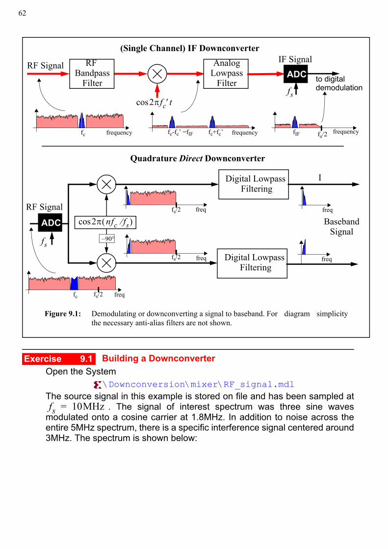
9 Direct Digital Downconversion
In this section we shall consider some of the hardware components required toimplement a digital down converter. A downconverter brings an RF (radiofrequency) signal down to an intermediate or baseband frequency. Ultimatelydownconversion consists of shifting the signal of interest to a lower frequency,removing unwanted signal components and sampling the desired informationsignal at a “reasonable” sampling rate.
This section is split into a number of exercises. Firstly we shall build adownconverter using standard Simulink blocks and using double precisionarithmetic. We shall then consider how to optimise each component forimplementation on an FPGA.
9.1 Downconversion using DSP
Figure 9.1 shows two common downconverter architectures. The first converts toan intermediate frequency (IF) and requires a further stage of demodulation tobring down to baseband. An additional stage is then required to demodulate thesignal to baseband. The second technique is known as direct downconversion. Inthis case the signal is demodulated directly from RF to baseband.
62
Building a DownconverterOpen the System
\Downconversion\mixer\RF_signal.mdlThe source signal in this example is stored on file and has been sampled at
. The signal of interest spectrum was three sine wavesmodulated onto a cosine carrier at 1.8MHz. In addition to noise across theentire 5MHz spectrum, there is a specific interference signal centered around3MHz. The spectrum is shown below:
2πfc′tcos
AnalogLowpass
RF Bandpass
RF SignalIF Signal
Quadrature Direct Downconverter
Digital Lowpass
RF SignalBaseband
Signal
Filtering
(Single Channel) IF Downconverter
2π nfc fs⁄( )cos
frequency frequencyfc fc-fc’ =fIF fc+fc’ frequencyfIF
90°–
freqfc
freq
freq
I
freq
freq
Figure 9.1: Demodulating or downconverting a signal to baseband. For diagram simplicitythe necessary anti-alias filters are not shown.
ADC
ADC
fs
fs
fs/2
fs/2
fs/2
fs/2
Digital Lowpass Filtering
FilterFilter to digital demodulation
Exercise 9.1
fs 10MHz=
639 Direct Digital Downconversion
Run the system and view the received signal. As shown above you should seetwo distinct components; the first centred on 1.8MHz comprises a number oftones. The second is an interfering signal centred on 3 MHz.
In order to gain an understanding of how a downconverter works we shall builda system using Xilinx System Generator blocks which will demodulate the1.8MHz component to baseband. The following steps should help you toachieve this.
(a) We can use a multiplier to mix down the signal to baseband using an1.8MHz cosine. Implement this or open the system in:
\Downconversion\mixer\mixer.mdlCan you account (by some pseudo-trigonometry) for the frequencycomponents which appear centered at 1.2MHz, 3.6MHz and 4.8MHz?What would happen if you mixed down with a sine-wave - Why would thisbe?
(b) Design a lowpass filter which retains the 1.8MHz component howeverremoves the 3MHz signal by at least 60dB. Filters can be designed usingthe Simulink Xilinx Blockset>Tools>FDATool. A designed filter canbe found in:
\Downconversion\mixer\lpfilter.mdl(c) Assuming the original signal can be considered to have a bandwidth of
1MHz, place a suitable downsampling at the output of the filter to decimateby 50. A designed filter can be found in:
\Downconversion\mixer\decimate.mdl(d) Confirm that the downconvert is functioning correctly, using System
Generator the take this final design through the ISE tools to an FPGAimplementation using the XCVP30 from the VIrtex II Pro family - does you
Signal of interest Interferer
0 1 2 3 4 5freq/MHz
-120
-180
Pow
er/d
B
64
design actually synthesise OK?
Any comments on the final design?
9.2 CICs for Downconversion
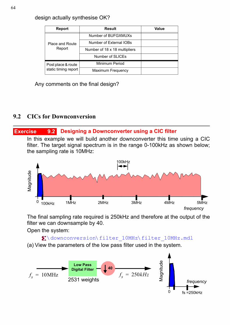
Designing a Downconverter using a CIC filterIn this example we will build another downconverter this time using a CICfilter. The target signal spectrum is in the range 0-100kHz as shown below;the sampling rate is 10MHz:
The final sampling rate required is 250kHz and therefore at the output of thefilter we can downsample by 40.Open the system:
\downconversion\filter_10MHz\filter_10MHz.mdl(a) View the parameters of the low pass filter used in the system.
Report Result Value
Place and Route Report
Number of BUFGXMUXs
Number of External IOBs
Number of 18 x 18 multipliers
Number of SLICEs
Post place & route static timing report
Minimum Period
Maximum Frequency
Exercise 9.2
frequency
Mag
nitu
de
1MHz 2MHz 3MHz 4MHz 5MHz0
100kHz
100kHz
Low Pass Digital Filter
fs 10MHz=2531 weights
40
fs 250kHz=frequencyM
agni
tude
fs =250kHz0
659 Direct Digital Downconversion
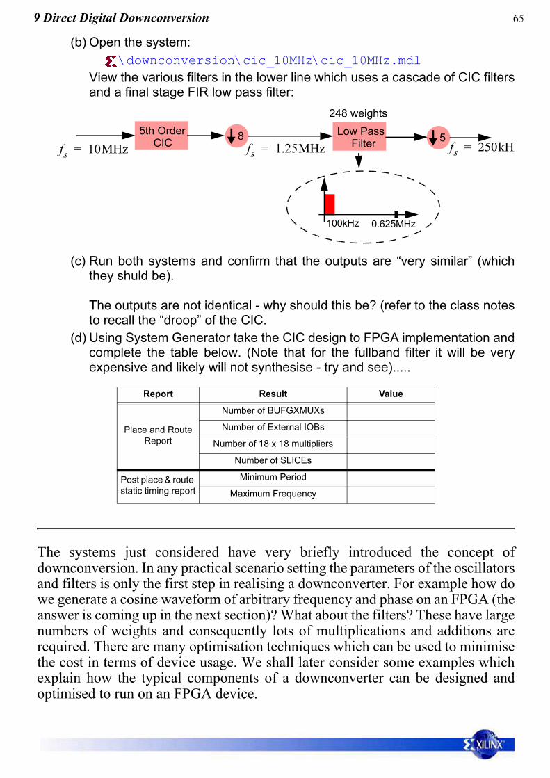
(b) Open the system:\downconversion\cic_10MHz\cic_10MHz.mdl
View the various filters in the lower line which uses a cascade of CIC filtersand a final stage FIR low pass filter:
(c) Run both systems and confirm that the outputs are “very similar” (whichthey shuld be).
The outputs are not identical - why should this be? (refer to the class notesto recall the “droop” of the CIC.
(d) Using System Generator take the CIC design to FPGA implementation andcomplete the table below. (Note that for the fullband filter it will be veryexpensive and likely will not synthesise - try and see).....
The systems just considered have very briefly introduced the concept ofdownconversion. In any practical scenario setting the parameters of the oscillatorsand filters is only the first step in realising a downconverter. For example how dowe generate a cosine waveform of arbitrary frequency and phase on an FPGA (theanswer is coming up in the next section)? What about the filters? These have largenumbers of weights and consequently lots of multiplications and additions arerequired. There are many optimisation techniques which can be used to minimisethe cost in terms of device usage. We shall later consider some examples whichexplain how the typical components of a downconverter can be designed andoptimised to run on an FPGA device.
Report Result Value
Place and Route Report
Number of BUFGXMUXs
Number of External IOBs
Number of 18 x 18 multipliers
Number of SLICEs
Post place & route static timing report
Minimum Period
Maximum Frequency
85th Order CIC
Low PassFilter
0.625MHz100kHz
5
248 weights
fs 10MHz= fs 1.25MHz= fs 250kHz=
66
10 Numerically Controlled Oscillators
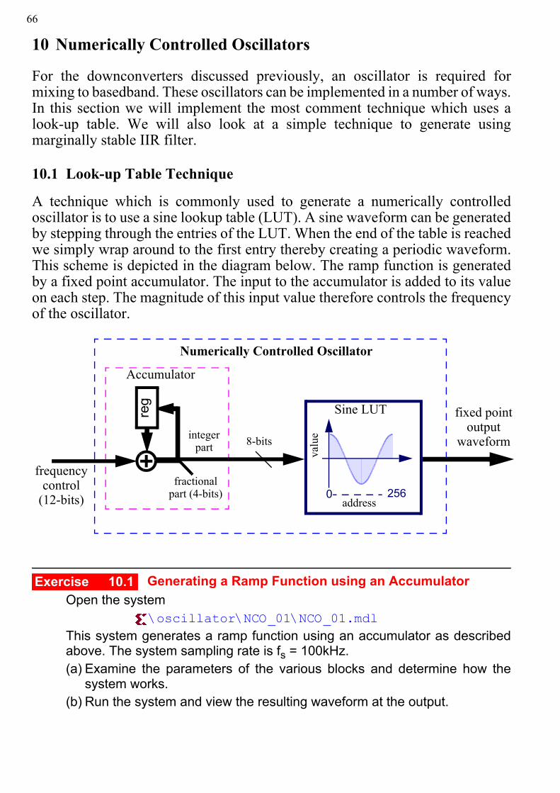
For the downconverters discussed previously, an oscillator is required formixing to basedband. These oscillators can be implemented in a number of ways.In this section we will implement the most comment technique which uses alook-up table. We will also look at a simple technique to generate usingmarginally stable IIR filter.
10.1 Look-up Table Technique
A technique which is commonly used to generate a numerically controlledoscillator is to use a sine lookup table (LUT). A sine waveform can be generatedby stepping through the entries of the LUT. When the end of the table is reachedwe simply wrap around to the first entry thereby creating a periodic waveform.This scheme is depicted in the diagram below. The ramp function is generatedby a fixed point accumulator. The input to the accumulator is added to its valueon each step. The magnitude of this input value therefore controls the frequencyof the oscillator.
Generating a Ramp Function using an AccumulatorOpen the system
\oscillator\NCO_01\NCO_01.mdlThis system generates a ramp function using an accumulator as describedabove. The system sampling rate is fs = 100kHz.(a) Examine the parameters of the various blocks and determine how the
system works.(b) Run the system and view the resulting waveform at the output.
0 256
reg
integerpart
frequencycontrol
Accumulator
Numerically Controlled Oscillator
Sine LUT
address
valu
e8-bits
fractionalpart (4-bits)(12-bits)
fixed pointoutput
waveform
Exercise 10.1
6710 Numerically Controlled Oscillators
(c) Derive an equation which determines the frequency of the resultingsawtooth waveform for a given step size. You may ignore numericalinaccuracy at this stage.
(d) Set the step size such that the sawtooth waveform has a frequency of1000Hz.
Effect of Accumulator PrecisionOpen the system
\oscillator\NCO_02\NCO_02.mdlThis system contains two fixed point ramp (sawtooth) generators. They areboth currently configured so that the accumulator has a precision of 8 integerbits and 2 fractional bits.(a) Run the system and view the outputs.(b) What do you think would be the effect of changing the precision (i.e. number
of fractional bits) of one of the ramp generators?(c) Set one of the function generators to have 6 fractional bits rather than 2.
This only requires you to change the gateway block. The adder isconfigured to use the same precision as its input.
(d) Run the system and view the results. Is this what you expected?
Generating a Sine Wave using a Lookup TableOpen the System
\oscillator\NCO_03\NCO_03.mdlThis system builds on the previous ones by introducing a sine lookup table. Thefractional part of the ramp signal is disregarded and the integer part is used toaddress the look-up table stored in memory.(a) Study the parameters of the converter block and the memory with the sine
wave. (b) Run the system and view the output. Note that the sawtooth wave and sine
wave have the same frequency.(c) Observe the frequency response of the sinusoid which is generated by the
NCO. Measure the approximate difference in power between the dominanttone and the harmonic tones.
(d) In the design, change the precision of the lookup table entries to 16 bits (i.e.16 bit register with 15 fractional bits). Run the system and view the newresults. Now measure the difference between the dominant tone and theharmonics. How does this compare to the measurement in (c)?
(e) Why do you think the quantisation noise appears as harmonics in thisexample?
Exercise 10.2
Exercise 10.3
68
(f) Leave the lookup table precision at 16 bits and change the frequency ofthe NCO to 1kHz by setting the step size to 2.56. Run the system again.What has happened to the power of the harmonics. Can you explain whyyou obtain this result?
10.2 Sine Wave Generation Using IIR Filters
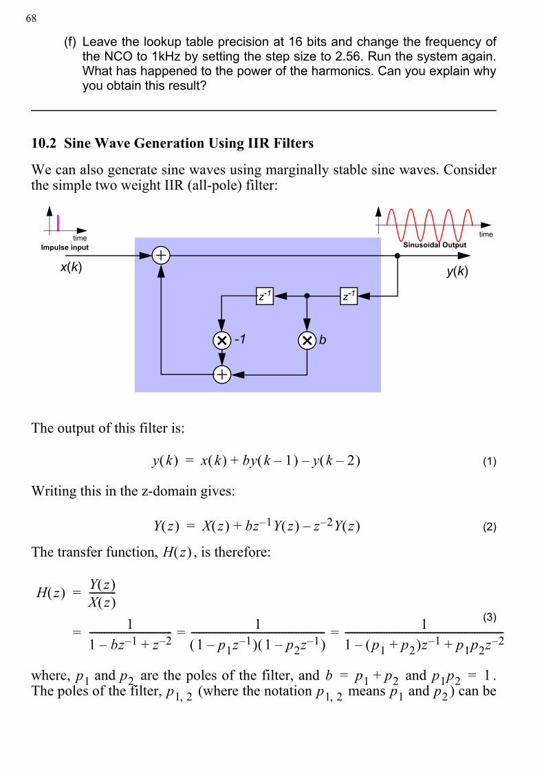
We can also generate sine waves using marginally stable sine waves. Considerthe simple two weight IIR (all-pole) filter:
The output of this filter is:
(1)
Writing this in the z-domain gives:
(2)
The transfer function, , is therefore:
(3)
where, are the poles of the filter, and and .The poles of the filter, (where the notation means ) can be
z-1z-1
x(k)
-1 b
y(k)
time time
Impulse input Sinusoidal Output
y k( ) x k( ) by k 1–( ) y k 2–( )–+=
Y z( ) X z( ) b+ z 1– Y z( ) z 2– Y z( )–=
H z( )
H z( ) Y z( )X z( )-----------=
11 bz 1–– z 2–+---------------------------------- 1
Given that is a real value, then are complex conjugates. RewritingEq. 4 in polar form gives:
(5)
Considering the denominator polynomial of Eq. 3, the magnitude of the complexconjugate values are necessarily both 1, and the poles will lie on theunit circle. In terms of the frequency placement of the poles, noting that this isgiven by:
(6)
(where for any ) for a sampling frequency , from Eq. 6 and Eq. 5 itfollows that:
(7)
Sine Wave Oscillators using IIR filtersOpen the system
\oscillator\sine_wave_iir.mdl
p1 2,b b2 4–±
2---------------------------- b j 4 b2–±
2------------------------------= =
b p1 and p2
p1 2, ej± 4 b2–
b------------------tan 1–
=
p1 and p2
p1 2, 1 ej2± πffs
--------------= =
ejω 1= ω fs
2πffs
-------- 4 b2–b
------------------tan 1–=
Exercise 10.4
70
In this example we have implemented an IIR filter sampling at fs = 100MHzwith b = 1.75
(a) Using the root-locus of facility of the Linear System block, confirm that thepoles of the filter are as shown above.
(b) Run the system observe the sine wave and the frequency spectrum of theIIR filters (implemented via a linear system block and also from discreteblocks) and confirm the frequency of the sine wave is 8.04MHz.
(c) From above the equation confirm thatthis is correct for b = 1.75.
(d) Change the value to b = 1.95 (note that in the Linear System block youtype in the coefficients of the z-polynomial therefore you will enter -1.95).Calculate the frequency of the output using the equation above. Confirmthis is correct by running the simulation.
(e) If we set b = 0, then:
what is the frequency of the output now? Run the simulation and observethe frequency of the signal. Observe the time domain signal (zoom in tosee individual periods.)
Sine Wave Oscillators using IIR filtersOpen the system\oscillator\sine_wave_iir_spectrum.mdl
z-1z-1
x(k)
-1 1.75
y(k)1
1
-1
-1Re
Im
z-domain
H z( ) 11 1.75z 1–– z 2–+-----------------------------------------=
2πf( ) fs⁄ 4 b2–( ) b⁄tan 1–=
H z( ) 11 z 2–+-----------------=
1
1
-1
-1Re
Imz-domain
Exercise 10.5
7110 Numerically Controlled Oscillators
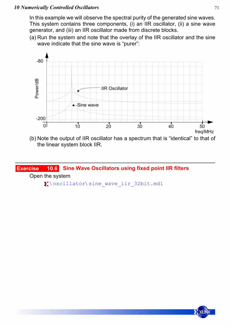
In this example we will observe the spectral purity of the generated sine waves.This system contains three components, (i) an IIR oscillator, (ii) a sine wavegenerator, and (iii) an IIR oscillator made from discrete blocks.(a) Run the system and note that the overlay of the IIR oscillator and the sine
wave indicate that the sine wave is “purer”:
(b) Note the output of IIR oscillator has a spectrum that is “identical” to that ofthe linear system block IIR.
Sine Wave Oscillators using fixed point IIR filtersOpen the system
\oscillator\sine_wave_iir_32bit.mdl
0 10 20 30 40 50freq/MHz
-80
-200
Pow
er/d
B
Sine wave
IIR Oscillator
Exercise 10.6
72
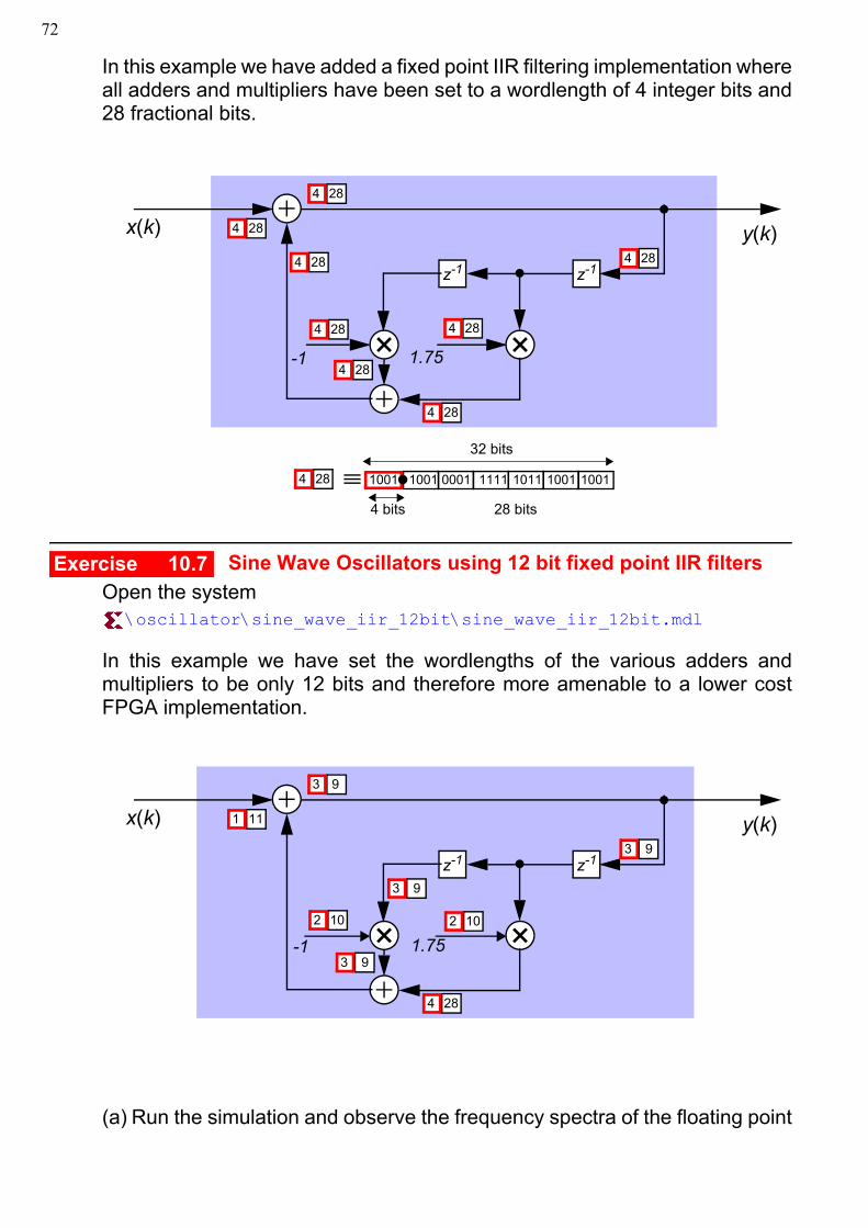
In this example we have added a fixed point IIR filtering implementation whereall adders and multipliers have been set to a wordlength of 4 integer bits and28 fractional bits.
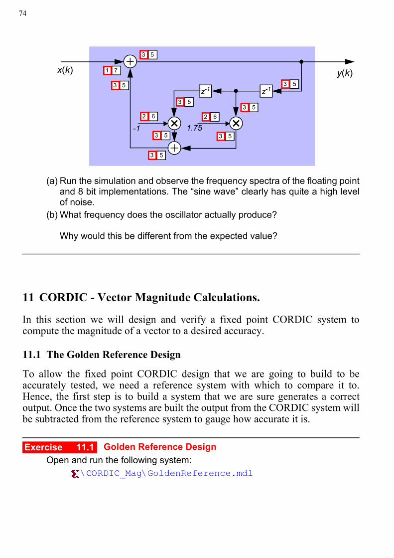
Sine Wave Oscillators using 12 bit fixed point IIR filters Open the system
In this example we have set the wordlengths of the various adders andmultipliers to be only 12 bits and therefore more amenable to a lower costFPGA implementation.
(a) Run the simulation and observe the frequency spectra of the floating point
1001 0001 1111 1011 100110011001
4 bits 28 bits
z-1z-1
x(k) y(k)4 28
4 28
4 28
4 28
4 28
4 28
4 28 4 28
32 bits
4 28
-1 1.75
Exercise 10.7
z-1z-1
x(k) y(k)1 11
3 9
3 9
3 9
4 28
2 10 2 10
-1 1.75
3 9
7310 Numerically Controlled Oscillators
and 12 bit implementations.(b) If you view the frequency spectra you should notice that the two spectra are
very similar but not identical. The 12 bit representation has slightly morenoise components visible (i.e. a less pure sine wave).
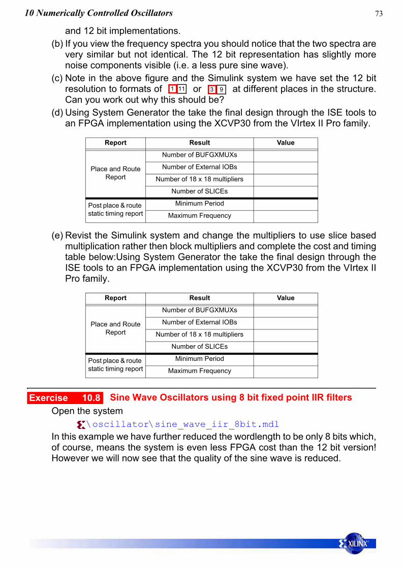
(c) Note in the above figure and the Simulink system we have set the 12 bitresolution to formats of or at different places in the structure.Can you work out why this should be?
(d) Using System Generator the take the final design through the ISE tools toan FPGA implementation using the XCVP30 from the VIrtex II Pro family.
(e) Revist the Simulink system and change the multipliers to use slice basedmultiplication rather then block multipliers and complete the cost and timingtable below:Using System Generator the take the final design through theISE tools to an FPGA implementation using the XCVP30 from the VIrtex IIPro family.
Sine Wave Oscillators using 8 bit fixed point IIR filtersOpen the system
\oscillator\sine_wave_iir_8bit.mdlIn this example we have further reduced the wordlength to be only 8 bits which,of course, means the system is even less FPGA cost than the 12 bit version!However we will now see that the quality of the sine wave is reduced.
Report Result Value
Place and Route Report
Number of BUFGXMUXs
Number of External IOBs
Number of 18 x 18 multipliers
Number of SLICEs
Post place & route static timing report
Minimum Period
Maximum Frequency
Report Result Value
Place and Route Report
Number of BUFGXMUXs
Number of External IOBs
Number of 18 x 18 multipliers
Number of SLICEs
Post place & route static timing report
Minimum Period
Maximum Frequency
1 11 3 9
Exercise 10.8
74
(a) Run the simulation and observe the frequency spectra of the floating pointand 8 bit implementations. The “sine wave” clearly has quite a high levelof noise.
(b) What frequency does the oscillator actually produce?
Why would this be different from the expected value?
11 CORDIC - Vector Magnitude Calculations.
In this section we will design and verify a fixed point CORDIC system tocompute the magnitude of a vector to a desired accuracy.
11.1 The Golden Reference Design
To allow the fixed point CORDIC design that we are going to build to beaccurately tested, we need a reference system with which to compare it to.Hence, the first step is to build a system that we are sure generates a correctoutput. Once the two systems are built the output from the CORDIC system willbe subtracted from the reference system to gauge how accurate it is.
Golden Reference DesignOpen and run the following system:
\CORDIC_Mag\GoldenReference.mdl
z-1z-1
x(k) y(k)1 7
3 5
3 5
3 5
2 6 2 6
-1 1.75
3 5
3 5
3 5
3 5
3 5
Exercise 11.1
7511 CORDIC - Vector Magnitude Calculations.
In this example we will see that floating point blocks have been used toimplement a Direct approach. Using floating point blocks we are sure that themagnitude that is computed will have a high degree of accuracy.(a) Change the input values of the Constant blocks and verify that the system
is actually computing the magnitude correctly.
11.2 The Fixed Point CORDIC Design
The fixed point CORDIC system that we are going to build will compute themagnitude of a vector to an accuracy of 5 effective fractional bits. The first stepis to consult the table below which predicts values of deff (the number of effectivefractional bits) for systems with n iterations and b fractional bits in the data path.
From the table it is clear that we could choose either n = 4, b = 7 or n = 3, b = 8 toobtain deff = 5. When faced with trading n for b, always choose the smallest n asthis offers the most efficient design.
One final parameter for our design that must be discussed is the maximummagnitude of the vector that will be rotated. The above table was generatedwith the assumption that the x and y inputs would be constrained to . Thismeans that the maximum value that the magnitude could be is and hence thisis the value that was used to generate the table. Thus, the inputs to our design mustbe in the range . Now that all the parameters required to build our system areknown, we can begin.
Set Up The Input SignalsStarting with the system in the previous exercise we shall now begin to buildthe fixed point CORDIC system. The first step is to put down the input signals. Reopen the system (same as previous exercise):
\CORDIC_Mag\GoldenReference.mdl
Predicted
n / b 7 8 9
1 2.21 2.24 2.26
2 3.51 3.62 3.68
3 4.74 5.09 5.31
4 5.31 6.03 6.59
5 5.36 6.28 7.13
6 5.23 6.21 7.17
v 0( )0.5±
0.5
0.5±
Exercise 11.2
76
and save it with a new filename to a desired location. This new file will be usedto build the CORDIC system.At this stage the reference design is driven by Constant blocks which providea source with a constant amplitude. However, we are now going to useUniform Random Number blocks to drive both the reference design and thefixed point CORDIC design that we will shortly build.(a) Drag in a Uniform Random Number block from the Simulink>Sources
library. Open up the block parameter window and set Minimum = -0.5 andMaximum = 0.5. Close the block by clicking the OK button.
(b) We need two of these blocks so to duplicate the original, right click on itand select Copy and then paste the block into the workspace. A secondUniform Random Number block with the same parameters will appear. Donot connect the new input blocks to anything yet.
(c) Rename both blocks to ‘x input’ and ‘y input’ and then save the file andcheck it against:
\CORDIC_Mag\CORDIC_mag1.mdlSet The Fixed Point Format Of The Input
The Uniform Random Number blocks created will produce floating point data.Hence, we must now convert these signals into a desired fixed point format.(a) Building on the previous system, drag in a Gateway In block from the Xilinx
Blockset>Basic Elements library. Open the block parameters window andset Number of Bits = 9 and Binary Point = 8. Make sure the Output DataType is set to Signed and close the block. Hence, the fixed point formatwill be .
(b) Again, we need two Gateway In blocks so duplicate the original.(c) Connect the Uniform Random Number blocks to the Gateway In blocks.(d) Save the file and check it against:
\CORDIC_Mag\CORDIC_mag2.mdlConnect The Fixed Point Inputs To The Reference Design
The fixed point inputs are used to drive both the reference design and theCORDIC design. Hence, the Constant blocks driving the reference design atpresent can be replaced by the fixed point inputs just created. However, thefloating point blocks of the reference design must be driven with floating pointdata. This means that the fixed point inputs must be converted back into afloating point format.(a) Delete the Constant blocks driving the reference design.(b) Drag in a Gateway Out block from the Xilinx Blockset>Basic Elements
library. Open the block parameters and uncheck the “Translate into OutputPort” option. Close the parameters and notice that the block has turnedgray.
Exercise 11.3
<1,8>±
Exercise 11.4
7711 CORDIC - Vector Magnitude Calculations.
(c) Then connect the Gateway Out block to one of the multipliers like so:
(d) Duplicate the Gateway Out block and connect the new block to the othermultiplier in the same fashion as above.
(e) Now connect the Gateway In blocks to the Gateway Out blocks. (f) Finally drag in a System Generator block from the Xilinx Blockset>Basic
Elements library. Save the design and check against:\CORDIC_Mag\CORDIC_mag3.mdl
Note that the reference design has simply been wrapped up into a subsystemwhich can be acheived easily by dragging a box around the blocks that are togo into the subsystem and then right clicking on the selected blocks andselecting Create Subsystem.
x Input ConverterIf the x input data is not controlled so that only positive values enter theCORDIC system, the magnitude will not be generated correctly. Hence, a smallcircuit must be designed to convert negative x input data to positive data.(a) Design the small circuit shown below using blocks from the Xilinx Blockset
library:
(b) Set the output of the Negate block to (Number of Bits = 9, BinaryPoint = 8).
(c) Make sure and check the “Boolean Output” option for the Slice block.(d) Set the output of the Mux block to .(e) Save the file and check against:
\CORDIC_Mag\CORDIC_mag4.mdlImport The First Cell
The cell that will compute the first iteration of the CORDIC system has alreadybeen developed and can be imported into your design and connected to theappropriate inputs.Open the file:
\CORDIC_Mag\Cell1.mdl
Exercise 11.5
x
<1,8>±
<1,8>±
Exercise 11.6
78
Open the cell and note that the circuit represents the following equations:
By opening the Shift blocks it can be seen that a right shift of 0 bits is set, asis required for the first iteration. The width of the data paths can all be seen tobe set to thus satisfying the 8 fractional bits that were specified inthe deff table. Note that 2 integer bits are required to accommodate the growthdue to the scaling factor K.(a) Copy the cell into your design.(b) Now connect the output of the Mux block to the x input of the cell.(c) Before connecting the y input to the Cell, insert a Delay block between the
y Gateway In block and the Cell. Then connect the y Gateway In block tothe Delay and the output from the Delay to the y input of the cell.
(d) Once again save the file and check against:\CORDIC_Mag\CORDIC_mag5.mdl
Note that the circuit built to convert the x input data into positive values hasbeen captured in a subsystem.
Create The Second CellThe initial cell can be used to generate any existing cells although it will haveto be altered appropriately.(a) Make a copy of the first cell and place it next to the original.(b) Connect the x output of cell 1 to the x input of cell 2 and do the same with
the y input/output of both cells.(c) Now edit both Shift blocks in the second cell so that the number of bits
shifted = 1.(d) Save the file and check against:
\CORDIC_Mag\CORDIC_mag6.mdlCreate The Third Cell
The second cell can now be used to create the third cell. This will be the finalcell that is required (n = 3 was given by the deff table).(a) Make a copy of the second cell and then connect the x output/input and y
output/input of both cells as done previously.(b) Open the third cell and edit both Shift blocks so that the number of bits
shifted = 2.(c) Save the file and check against:
\CORDIC_Mag\CORDIC_mag7.mdl
x 1( ) x 0( ) di 2 0– y 0( )( )–( )=
y 1( ) y 0( ) di 2 0– x 0( )( )+( )=
<2,8>±
Exercise 11.7
Exercise 11.8
7911 CORDIC - Vector Magnitude Calculations.
Add The Post Scaling MultiplierNow that all the cells have been implemented, all that remains of the CORDIChardware is the post scaling multiplier and the constant source generating 1/K. (a) Drag in a Multiplier block and a Constant block from the Xilinx Blockset
library.(b) Connect the Constant block to one of the Multiplier inputs.(c) Connect the x output from cell 3 to the other Multiplier input.(d) Set the parameters of the Multiplier block according to:(e) Set the output of the Constant block to and enter the desired value
to 1/1.62980060130066, which is equal to 1/K(3). Also check the “SampledConstant” option.
Exercise 11.9
<1,8>±
80
(f) Drag in a Delay block and connect it to the output from the Multiplier.(g) Finally select all the fixed point CORDIC blocks (by dragging a box around
them) and put them into a subsystem.(h) Save the file and check it against:
\CORDIC_Mag\CORDIC_mag8.mdlSubtract CORDIC Output From Reference Signal
To obtain the error of the CORDIC system, its output must be subtracted fromthe output of the reference system. However, the reference system outputs afloating point signal so the CORDIC output must also be converted to floatingpoint format before subtracting it. Also, we need to compensate for any delaysso that both the reference output and the CORDIC output are synchronised.(a) Drag in a Gateway Out block and connect it to the output of the CORDIC
subsystem.(b) Drag in an Integer Delay block from the Simulink>Discrete library. Open
up the parameters of the block and set Number of Delays = 1. Then,connect the input of this block to the output of the Gateway Out block.
(c) The delay through the entire CORDIC data path is now 3 clock periods.Hence, we must delay the reference signal by the same amount. Copy theInteger Delay block and change its parameters to Number of Delays = 3.Connect the output of the reference subsystem to the input of this delay.
(d) Now drag in an Add block from the Simulink>Math Operations library.Open up the parameters of this block and set them to:
(e) Connect the delayed output from the reference system to the + port of theAdd block and connect the delayed output from the CORDIC system to the- port of the Add block.
(f) Now drag in an Abs block from the Simulink>Math Operations library andconnect it to the output of the Add block.
Exercise 11.10
8111 CORDIC - Vector Magnitude Calculations.
(g) Next, drag in a MinMax Running Resettable block from the Simulink>MathOperations library and set its parameters to Function = max. Connect theoutput of the Abs block to the input of this block. You do not need to connectthe R port to anything.
(h) Finally, to view the output, drag in a Scope block from the Simulink>Sinkslibrary and then connect the output of the Add block to the input of theScope block. This will show all the errors. To view the max absolute error,drag in a Display block from the Simulink>Sinks library and connect it to thethe MinMax block. Set the parameters of the this sink to Format = long_e.This will show the maximum absolute error for the simulation.
(i) Save the system and check it against:\CORDIC_Mag\CORDIC_mag9.mdl
Run The SystemNow the system is ready to be run.(a) Run the system by clicking on the button on the Simulink toolbar.(b) Wait for the simulation to finish and then view the absolute error by double
clicking on the Scope block. The maximum absolute error will be shown inthe display block.
(c) We now need to compute . This will give usthe number of effective fractional bits.
(d) Perform this calculation using the value given in the Display. The followingequation may be useful:
(e) Confirm that the number of effective fractional bits is > 5 as was specifiedat the start by the deff table.
(f) Change the length of the simulation and the seeds for the Uniform RandomNumber generators and reconfirm that 5 effective bits are still acheived.
11.3 Build A Fixed Point CORDIC System.
Build A CORDIC System To Compute deff = 10.(a) Using the system that was built to compute deff = 5 as a template, build
another system to compute deff = 10. Use the table below to help find theparameters that you will need. As before, this table was generated for
. Verify the accuracy of your design using a floating point
Exercise 11.11
log2 Max Absolute Error( )–
log2xlog10xlog102----------------=
Exercise 11.12
v 0( ) 0.5=
82
reference design.
The following values may be useful:K(5) = 1.64568891575726, K(6) = 1.64649227871248, K(7) = 1.64669325427364, K(8) = 1.64674350659690Once your system is complete, save it and check it against:
\CORDIC_Mag\CORDIC_deff10.mdlHow does your system compare? Have you managed to obtain deff = 10 withless iterations? Also, have you noticed that the final cell can be reduced to halfthe logic of the other cells because the y output is not required?
11.4 Using CORDIC In A QR-Array
In this section we are going to see how the CORDIC systems that have just been
n / b 11 12 13 14 15 16 17
3 5.50 5.53 5.55 5.56 5.56 5.56 5.56
4 7.22 7.36 7.44 7.48 7.50 7.51 7.51
5 8.47 8.90 9.17 9.33 9.41 9.46 9.48
6 8.97 9.74 10.37 10.83 11.12 11.30 11.40
7 9.01 9.94 10.83 11.62 12.27 12.76 13.08
8 8.90 9.89 10.86 11.80 12.69 13.50 14.18
9 8.77 9.77 10.76 11.75 12.72 13.67 14.57
10 8.65 9.65 10.65 11.64 12.64 13.63 14.60
8311 CORDIC - Vector Magnitude Calculations.
built can be used in a QR-array.
Using the diagram above we can see that the function of each boundary cell (BC)is to rotate an input vector (x,y) onto the x-axis. Hence, the new x value (x’) isequal to the magnitude of the initial vector and the new y value (y’) is 0. However,each boundary cell must pass on the angle θ to the other cells in its row. Thefunction of each remaining cell in the row is to rotate an input vector by the sameangle θ as the boundary cell. One way to do this is to have each boundary cellcompute cosθ and sinθ and pass these values on instead of θ itself. This meansthat each of the remaining cells in a row must only perform 4 multiplications and2 additions/subtractions to perform the rotation. The added benefit of thisapproach is that each boundary cell must compute the magnitude of the initialvector anyway to obtain x’. To obtain cosθ and sinθ then involves inverting themagnitude and multiplying it by x and y respectively.
0
0
0
R00 R01 R02
R11 R12
R22
d0 d1 d2
BC
BC
BC
BC
xy
cos θsin θ
y’ = 0
x’
x' x θcos y θsin+ x2 y2+= =y' y θcos x θsin– 0= =
θcos x x2 y2+( )⁄=
θsin y x2 y2+( )⁄=
y
xθ
magnitude
x’
84
QR Boundary Cell1In this exercise we are simply going to look at one implementation of a QRboundary cell. Note that the vector magnitude is computed with 9 effectivefractional bits. Open the file:
\CORDIC_Mag\QR_BoundCell1\QR_BoundCell1.mdl(a) Open the CORDIC QR Boundary Cell subsystem and explore its contents.
Notice that the same architecture has been used to generate themagnitude as was used in the previous exercises.
(b) Run the system and take a note of the max errors for both Cos and Sin.
QR Boundary Cell2The system used in this exercise is exactly the same as the previous oneexcept that the vector magnitude is computed with 16 effective fractional bitsas opposed to 9. Open the file:
\CORDIC_Mag\QR_BoundCell2\QR_BoundCell2.mdl(a) Open the subsystems and confirm that the system is the same as the
previous exercise with the exception of the CORDIC magnitude unit.(b) Run the system and take a note of the max errors for both Cos and Sin
again. What do you notice?The fact that the CORDIC vector magnitude is computed to 16 effective bitsrather than 9 has had a dramatic effect on the accuracy of the values of Cosand Sin. In the previous exercise the Cos and Sin were generated withapproximately 6 effective bits. However, now that the accurcay of themagnitude has been improved, Cos and Sin are now generated with 11effective bits. The QR algorithm is sensitive to quantisation so it is importantto know where we can improve the accuracy of the algorithm.
The Cost Of A QR Boundary CellUsing System Generator and ISE the hardware for the previous system hasbeen generated, synthesised and implemented. This was done to save timeas the process can be quite lengthy. However, feel free to go through eachstage on your own. To view the ISE project that was generated open:
(a) Explore the project and take a look at the cost of the hardware by viewingthe Place & Route Report. You should see the following:
Exercise 11.13
Exercise 11.14
Exercise 11.15
8512 Fixed Point Sigma-Delta
(b) The speed at which the design can be clocked at can be found in the Text-based Post-Place & Route Static Timing Report. The timing summary isgiven below:
12 Fixed Point Sigma-Delta
This section demonstrates on sigma delta techniques using fixed point arithmetic.It is recommended that the section on sigma delta principles of the DSPedia iscovered before going through the examples below
The sequence of examples presented next implement a fixed point arithmeticsigma delta converter for an audio application. It is important to note that thisexample considers feedback issues. Under these conditions the designer has totake into account certain points which are highlighted in the examples below.
10 bit to 1bit oversampling Sigma DeltaOpen the system.
\sigmadelta\SigmaDelta01\SigmaDelta01.mdlThe one bit oversampled sigma delta signal is low pass filtered anddownsampled in order to produce the original signal.(a) Run the simulation view the 1 bit output of the sigma delta oversampler.(b) Using System Generator the take the final design through the ISE tools to
an FPGA implementation using the XCVP30 from the VIrtex II Pro family.
Report Result Value
Place and Route Report
Number of BUFGXMUXs
Number of External IOBs
Number of 18 x 18 multipliers
Number of SLICEs
Post place & route static timing report
Minimum Period
Maximum Frequency
Exercise 12.1
86
13 Fixed Point Bandlimiting: RRC Filtering
It is very important to make sure a transmitter only uses its assigned bandwidth.It is normally the role of the pulse shaping filter to limit the bandwidth of thetransmitted signal so it does not leak into adjacent frequency bands. In order toensure this the pulse shaping filter has to be designed properly.
Very often the amount of power that can be leaked into adjacent bands is givenas a frequency mask as shown below. This mask specifies the maximum powerlevels which are allowed in the frequency band of interest and adjacent channels.
If the spectrum at the output of a pulse shaping filter does not meet the frequencymask requirements the amount of power leaked into adjacent bands larger thanallowed and the filter does not meet the specifications. An example of this isgiven below, where filter B does not meet the mask but filter A does.
freq
Power spectraldensity
frequency mask
band ofinterest
pulseshapingfilter A
pulseshapingfilter B
mask NOT met
8713 Fixed Point Bandlimiting: RRC Filtering
A filter designed with floating point precision will change its characteristic whenits coefficients are quantised. Thus, a filter operating correctly and meeting themask in floating point may be unsuitable once its coefficients have beenquantised.
The next sequence of examples shows how the frequency response of a pulseshaping filter changes as its weights are quantised with different number of bits.
64QAM Sequence GenerationOpen the system.
\PulseShape\64QAM_01.mdlThis system shows the mapping of a sequence of symbols onto a 64QAMconstellation. The original sequence of symbols has 64 levels and is generatedat a rate of . Since 64 levels can be represented with 6 bitsthe total bit rate is .(a) Run the simulation and i check the produced constellation.
Quantisation of 64QAM ConstellationOpen the system.
\PulseShape\64QAM_02.mdlIn this example the generated 64QAM constellation is quantised andrepresented in fixed point precision using 8 integer bits signed format (<8,0>signed).(a) Run the simulation and check the produced constellation.
RRC Filter: Floating Point WeightsOpen the system.
\PulseShape\64QAM_03.mdlA certain RRC filter design has been chosen and used in this example. The In-phase and quadrature components generated (I & Q) are independently filteredwith two real RRC filters. The coefficients of these filters are represented withdouble precision.(a) Open the filters parameter box and check that they both have the same
impulse response, i.e. they are the same filter. Observe the filters frequencyresponse.
(b) Run the simulation, and observe the spectrum of the generated signal. Is itsimilar to the frequency response of the filters used?
RRC Filter: 12-bit Weights, 20-bit OutputOpen the system.
\PulseShape\64QAM_04.mdl
Exercise 13.1
28 Msymbols/sec28 6× 168 Mbits/sec=
Exercise 13.2
Exercise 13.3
Exercise 13.4
88
In this example fixed point filters are used. The coefficients of the RRC filterhave been quantised using 12 bits while the output of the filter is representedusing 20 bits.(a) Open the fixed point filter parameter box and check that the wordlengths
used are the ones indicated above.(b) The gain blocks after the fixed point filters compensate for differences in
amplitude between the two systems and have been used only to simplifythe visual analysis of the results.
(c) Run the simulation and observe the results. The automated sequence willcalculate the spectrum of the output of both implementations (floating pointand 20-bit coefficients), and will overlay them. An averaging is performedso the differences can be more easily observed. Observe the differencesbetween the two produced spectra plots.
RRC Filter: 8-bit Weights, 16-bit OutputOpen the system.
\PulseShape\64QAM_05.mdlIn this example the number of bits used to represent the weights and the filteroutput has been reduced. The coefficients are now represented with 8 bitswhile the output of the filter is coded using 16 bits. Note that gain blocks havebeen used again to normalise the output of the filters.(a) Open the fixed point filter parameter box and check that the wordlengths
used are the ones indicated above.(b) Run the simulation and view the spectrum at the output of the different
filters.(c) Observe the differences in the spectrum.(d) Using System Generator the take the final design through the ISE tools to
an FPGA implementation using the XCVP30 from the VIrtex II Pro family.
RRC Filter: 5-bit Weights, 13-bit OutputOpen the system.
\PulseShape\64QAM_06.mdl
Report Result Value
Place and Route Report
Number of BUFGXMUXs
Number of External IOBs
Number of 18 x 18 multipliers
Number of SLICEs
Post place & route static timing report
Minimum Period
Maximum Frequency
Exercise 13.5
Exercise 13.6
8914 FPGA as an ASIC - Digital Downconverter
The number of bits used to represent the weights and the filter output has beenreduced even further. The coefficients are now represented with 5 bits whilethe output of the filter is coded using 13 bits. (a) Run the simulation and view the results. Observe the overlay of the
spectrum at the output of the different filters after the automated sequencehas been executed.
(b) What is the main effect in the spectrum when the wordlength used torepresent weights and outputs is reduced?
(c) Observe the differences in the spectrum. Which implementations meet themask specified below?
(d) Using System Generator the take the final design through the ISE tools toan FPGA implementation using the XCVP30 from the VIrtex II Pro family.
How does this compare to the cost from the previous exercise with thesmaller wordlength?
14 FPGA as an ASIC - Digital Downconverter
In this sequence of examples a digital downconverter is constructed in Simulink.
Report Result Value
Place and Route Report
Number of BUFGXMUXs
Number of External IOBs
Number of 18 x 18 multipliers
Number of SLICEs
Post place & route static timing report
Minimum Period
Maximum Frequency
freq (MHz)
Power spectraldensity
14 dB
21.517.7
90
As a quick view the general DSP structure of the system is shown below:
The examples demonstrate the digital downconversion of two modulatedinformation signals, and . These signals arrive at the input to the digitaldownconverter modulated onto the in-phase and quadrature components of a3.3MHz intermediate frequency (IF). The diagram below shows a simplifiedmodel of the system which will be constructed. The sampling rate at the input tothe downconverter is 12.8Msps however at the output this rate is reduced to200ksps and the unwanted channels are removed from the signal.
In the simulations almost all of the signals are represented using bit signed
HALFBAND
POLYPHASEFIR AND
FILTERS
INP
UT
SE
CT
ION
LEVEL DETECT
CARRIER
5TH
CARTESIANTO
OU
TP
UT
FO
RM
AT
TE
R
DISCRIMINATOR
AGC LOOP FILTER
MAG.
PHASE
RESAMPLING
I OUT
Q OUT
FREQ
AGC
∆TIMING ERROR
IN(13:0)
REFCLK
SEROUTA
SEROUTB
AOUT(15:0)
BOUT(15:0)
CONTROLC(7:0)
MICROPROCESSORREAD/WRITE
GAIN
(2:0)
HA
LFB
AN
DF
ILT
ER
S
FILTERCIC
ORDER
HA
LFB
AN
DF
ILT
ER
S
POLAR
COORDINATECONVERTER
HALFBAND
POLYPHASEFIR AND
FILTERS
NCO
NCOCOF
SOF
ADJ
CLKINPROCCLK
255-
TAP
FIR
FIL
TE
R25
5-TA
PF
IR F
ILT
ER5TH
FILTERCIC
ORDER
Figure 14.1: Digital Downconverter DSP functional block diagram.
I t( ) Q t( )
I t( )
Q t( )
sin
cos
3.3MHzOscillator
other frequencymultiplexed
channels
sin
cos
3.3MHzNCO
decimationfilters
Digital Downconverter
I n[ ]
Q n[ ]
Model of input signal to(Equivalent Model)digital downconverter
decimationfilters
fs =fs 200ksps=
12.8MHz
gain
gain
N
9114 FPGA as an ASIC - Digital Downconverter
fixedpoint values interpreted as having integer bit and fractional bits(denoted as <1,F> format). This format allows values in the range
to be represented. The bit weightings of this format are shownin the diagram below.
Bandlimited Information SignalsOpen the system
\qam-ddc\Downconverter_01.mdlThis system reads a pair of pre-generated bandlimited information signals intoSimulink from external files.
(a) Run the system and estimate the bandwidth occupied by these signals.1
Modulation of Information Signals onto IF CarrierOpen the system
\qam-ddc\Downconverter_02.mdlIn this system the I and Q waveforms are modulated onto a 3.2MHzintermediate frequency (IF) carrier signal. A model of the adjacent channelshas also been added.
(a) Inspect the new blocks and their parameters.(b) Run the system.(c) Now view the resulting signal at the output of the generator. Notice how it
looks like random noise.(d) View the spectrum and you should be able to see the signal of interest
centred on the carrier frequency and surrounded by noise representing theother channels.
23
Numerically Controlled OscillatorOpen the system
\qam-ddc\Downconverter_03.mdl
1 F N 1–=
1– x 1 2 F––≤ ≤
20 2 1– 2 2– 2 3– 2 F–
integer / sign bit fractional bits
Bit weighting of the <1,F> signed fixedpoint format
Exercise 14.1
Exercise 14.2
Exercise 14.3
92
In this system the received signal is mixed down to baseband using anumerically controlled oscillator (NCO) and two multipliers. The NCOgenerates sinusoidal signals by using an accumulator to generate a variablefrequency ramp function. The ramp function is then used to address a sineLook-Up Table (LUT). The result is a variable frequency digital oscillator. Ablock diagram of the NCO is shown below.
(a) Inspect the blocks which form the NCO and the mixer. Pay particularattention to the number of bits used at each stage.
(b) Run the system and view the various signals produced.
Note that the signal has now been mixed down to baseband however thenoise components are still there.
CIC FilterOpen the system
\qam-ddc\Downconverter_04.mdlIn this example a 5-stage CIC filter has been added to begin thedownsampling process. This reduces the sampling rate by a factor of 16 andremoves a significant proportion of the adjacent channels.(a) Run the system.(b) Compare the in-phase transmitted signal to the in-phase signal at the
output of the CIC filter. Does there appear to be any correlation betweenthe two?
Halfband FiltersOpen the system
\qam-ddc\Downconverter_05.mdl
32-bit unsignedphasestep
18 MSBs32 218 pointsinewave
LUTsize
18 sinewaveout
accumulator
Numerically controlled Oscillator
(frequencycontrol)
Exercise 14.4
Exercise 14.5
9314 FPGA as an ASIC - Digital Downconverter
Although CIC filters are an efficient to perform decimation in a downconverterthey may only be used to reduce the rate to a certain degree due to the problemknown as “CIC droop”. CIC droop can modify the frequency content of ourchannel of interest and lead to inter-symbol interference.In our downconverter system the CIC brings the sampling rate down to 8x thesymbol rate. The remaining downconversion is performed using an FIR“halfband” filter and a programmable FIR filter.
(a) View the parameters of the two new filter blocks which have been added. Inparticular view the “weights” property page and view the impulse andfrequency responses of the filters. Why are these called “halfband” filters?Note that every second weight is zero (except for the middle weight) andhence these should lead to cheaper implementation.
(b) Now compare the transmitted and received information signals. What doyou notice about the signal levels. Remember that the input to theDownconverter is scaled to utilize the full dynamic range.
Active Gain ControlAs was seen in the previous example, the output of all of the filtering stagescan be a signal with relatively low amplitude. This is because all of the adjacentchannels (which form the majority of the downconverter input) have beenrejected. The Active Gain Control (AGC) stage is used to amplify the signal sothat it utilizes the dynamic range of the output word.
The gain part of the AGC loop has been included in this final simulation. Itconsists of a shift and a multiplier as shown in the diagram below. Theexponent controls the shift and therefore provides gains which are powers of2. The mantissa may be used to implement non-power of 2 gains. The overallgain is
The exponent is a number between 0 and 15 and the mantissa is a numberbetween 0 and .
(a) Inspect the parameters of the gain section in the system.(b) Calculate the total gain in dB which is introduced.(c) Now run the system and view the results.(d) Using System Generator the take the final design through the ISE tools to
an FPGA implementation using the XCVP30 from the VIrtex II Pro family.