March, 2003 IEEE P802.15-03/142r0 IEEE P802.15 Wireless Personal Area Networks Project IEEE P802.15 Working Group for Wireless Personal Area Networks (WPANs) Title TI Physical Layer Proposal for IEEE 802.15 Task Group 3a Date Submitt ed 03 March, 2003 Source [Anuj Batra et al.] [Texas Instruments, Inc.] [12500 TI Blvd, Dallas, TX 75243] Voice: [214-480-4220] Fax: [972-761-6966] E-mail: [[email protected]] Re: [If this is a proposed revision, cite the original document.] [If this is a response to a Call for Contributions, cite the name and date of the Call for Contributions to which this document responds, as well as the relevant item number in the Call for Contributions.] [Note: Contributions that are not responsive to this section of the template, and contributions which do not address the topic under which they are submitted, may be refused or consigned to the “General Contributions” area.] Abstrac t A high rate WPAN with data rates from 55 Mbps to 480 Mbps is proposed. Submission Page 1 Anuj Batra et al., Texas Instruments, Inc.
Transcript
March, 2003 IEEE P802.15-03/142r0
IEEE P802.15Wireless Personal Area Networks
Project IEEE P802.15 Working Group for Wireless Personal Area Networks (WPANs)
Title TI Physical Layer Proposal for IEEE 802.15 Task Group 3a
Date Submitted
03 March, 2003
Source [Anuj Batra et al.][Texas Instruments, Inc.][12500 TI Blvd, Dallas, TX 75243]
Re: [If this is a proposed revision, cite the original document.]
[If this is a response to a Call for Contributions, cite the name and date of the Call for Contributions to which this document responds, as well as the relevant item number in the Call for Contributions.]
[Note: Contributions that are not responsive to this section of the template, and contributions which do not address the topic under which they are submitted, may be refused or consigned to the “General Contributions” area.]
Abstract A high rate WPAN with data rates from 55 Mbps to 480 Mbps is proposed.
Purpose Discussion
Notice This document has been prepared to assist the IEEE P802.15. It is offered as a basis for discussion and is not binding on the contributing individual(s) or organization(s). The material in this document is subject to change in form and content after further study. The contributor(s) reserve(s) the right to add, amend or withdraw material contained herein.
Release The contributor acknowledges and accepts that this contribution becomes the property of IEEE and may be made publicly available by P802.15.
Submission Page 1 Anuj Batra et al., Texas Instruments, Inc.
March, 2003 IEEE P802.15-03/142r0
Physical Layer Submission to 802.15 Task Group 3a:
Time-Frequency Interleaved Orthogonal Frequency Division Multiplexing
(TFI-OFDM)
Anuj Batra, Jaiganesh Balakrishnan, Anand DabakRanjit Gharpurey, Paul Fontaine, Jerry Lin
Jin-Meng Ho, Simon Lee
Texas Instruments, Inc.12500 TI Blvd, M/S 8649
Dallas TX 75243
March 11, 2003
Submission Page 2 Anuj Batra et al., Texas Instruments, Inc.
March, 2003 IEEE P802.15-03/142r0
Executive Summary
For initial deployment (quick time to market) of the proposed UWB systems, and development of low cost, low power CMOS solutions we propose to employ only three bands with bandwidth 528 MHz each and center frequencies 3432, 3960 and 4488 MHz respectively. The proposed system can in fact support up to a total of 14 bands, each with a bandwidth of 528 MHz and with center frequencies that range from 3432 MHz to 10296 MHz. Due to larger propagation loss at higher frequencies, only marginal gains are found by including the higher bands, which can be added in the future as RF technology improves. We employ time-frequency interleaving across the bands and employ orthogonal frequency division multiplexing (TFI-OFDM) with BPSK/QPSK modulation on the tones. Each OFDM symbol occupies a minimum of 500 MHz bandwidth at all times, as required by the FCC.
Employing OFDM for modulation allows the TFI-OFDM to be viewed as both a full-band and a sub-band system. Hence TFI-OFDM inherits advantages from both the full-band and sub-band UWB systems. Further, by appending a guard interval after the OFDM symbol, sufficient time (9.5 ns) is provided to allow both the transmitter and receiver to switch from one band to another. This allows a single transmit and receive analog chain at the receiver at all times, while still collecting significant multi-path energy. The proposed UWB system provides a wireless PAN with data payload communication capabilities of 55, 80, 110, 160, 200, 320, and 480 Mb/s. A summary of the TFI-OFDM system is as follows:
Average transmit power : The average transmit power is –10.3 dBm per band. Receiver sensitivity : The receiver sensitivity for 110 Mbps is –80.0 dBm. Range : The range for 110 Mbps in AWGN is 19.1 m and 9.7 m in CM3 multi-path channels. Power consumption: The total transmit power consumption for 110 Mbps is 93 mW, the total
receive power consumption for 110 Mbps is 142 mW in 90 nm technology and 15 W in deep sleep.
CMOS implementation : Since only the lower bandwidth (3.1 GHz – 4.8 GHz) is going to be used in the initial deployment of UWB systems, the proposed TFI-OFDM system can be built completely in current CMOS technology.
U-NII interference suppression : Since the TFI-OFDM system completely avoids all transmission in the U-NII band, the front-end filter design for rejecting interference from the U-NII band is simplified.
TFI-OFDM requires only one transmitter chain and one receiver chain at all times : The guard interval between OFDM symbols ensures that only one transmit chain is needed to generate the TFI-OFDM waveform and that a single RF chain is sufficient to receive at all times despite collecting significant multi-path.
Early time-to-market : The majority of the TFI-OFDM system can be implemented in standard digital CMOS logic and the analog implementation complexity can be minimized, which results in an early time-to-market.
Compliance with worldwide regulations/compliance with future systems : Channels and individual tones can be dynamically turned on and off in order to comply with changing regulations.
Antenna is easier to design : OFDM has an inherent robustness against gain, phase, and group delay variation that may be introduced by a broadband antenna.
Submission Page 3 Anuj Batra et al., Texas Instruments, Inc.
1.1.1 Choice of bandwidth for the proposed UWB system.............................................................................71.1.2 Time-frequency interleaved OFDM.......................................................................................................9
1.1.2.1 TFI-OFDM as a full-band system.....................................................................................................101.1.2.2 TFI-OFDM as a sub-band system.....................................................................................................121.1.2.3 Advantages of a TFI-OFDM system.................................................................................................14
1.1.3 Overview of the proposed UWB system description............................................................................151.1.3.1 Mathematical description of the signal.............................................................................................151.1.3.2 Discrete-time implementation considerations...................................................................................16
1.2 UWB PHY specific service parameter list....................................................................................................181.2.1 Introduction...........................................................................................................................................181.2.2 TXVECTOR parameters.......................................................................................................................18
1.3.5.1 Date rate (RATE)..............................................................................................................................271.3.5.2 PLCP length field (LENGTH)..........................................................................................................271.3.5.3 PLCP scrambler field (SCRAMBLER)............................................................................................28
1.3.6 Data scrambler......................................................................................................................................281.3.7 Tail bits.................................................................................................................................................291.3.8 Convolutional Encoder.........................................................................................................................291.3.9 Pad bits..................................................................................................................................................331.3.10 Bit interleaving......................................................................................................................................341.3.11 Subcarrier constellation mapping.........................................................................................................341.3.12 Pilot subcarriers....................................................................................................................................361.3.13 OFDM modulation................................................................................................................................36
1.4 General requirements....................................................................................................................................39
Submission Page 4 Anuj Batra et al., Texas Instruments, Inc.
March, 2003 IEEE P802.15-03/142r0
1.4.1 Operating channel frequencies..............................................................................................................391.4.1.1 Operating frequency range................................................................................................................391.4.1.2 Channel numbering...........................................................................................................................39
1.4.2 PHY layer timing..................................................................................................................................401.4.2.1 Interframe spacing............................................................................................................................401.4.2.2 Receive-to-transmit turnaround time................................................................................................401.4.2.3 Transmit-to-receive turnaround time................................................................................................401.4.2.4 Time between successive transmissions...........................................................................................411.4.2.5 Channel switch time..........................................................................................................................41
1.5.1 Transmit PSD mask..............................................................................................................................421.5.2 Transmit center frequency tolerance.....................................................................................................421.5.3 Symbol clock frequency tolerance........................................................................................................421.5.4 Clock synchronization..........................................................................................................................42
1.6 Receiver specification...................................................................................................................................431.6.1 Receiver sensitivity...............................................................................................................................431.6.2 Receiver CCA performance..................................................................................................................43
2 Self evaluation matrix.......................................................................................................................................442.1 General solution criteria................................................................................................................................442.2 PHY protocol criteria....................................................................................................................................452.3 MAC protocol enhancement criteria.............................................................................................................46
3 Detailed responses to selection criteria and self-evaluation matrix..................................................................473.1 Unit manufacturing cost................................................................................................................................473.2 Signal robustness..........................................................................................................................................47
3.2.2 Interference and susceptibility..............................................................................................................473.2.2.1 Microwave oven................................................................................................................................483.2.2.2 Bluetooth and IEEE 802.15.1 interferer...........................................................................................483.2.2.3 IEEE 802.11b and IEEE 802.15.3 interferer.....................................................................................483.2.2.4 IEEE 802.11a interferer....................................................................................................................483.2.2.5 IEEE 802.15.4 interferer...................................................................................................................493.2.2.6 Generic in-band modulated interferer...............................................................................................493.2.2.7 Generic in-band tone interferer.........................................................................................................493.2.2.8 Out-of-band interference from intentional and unintentional radiators............................................49
3.3 Technical feasibility......................................................................................................................................503.3.1 Manufacturability..................................................................................................................................503.3.2 Time to market......................................................................................................................................503.3.3 Regulatory impact.................................................................................................................................51
4 Alternate PHY required MAC enhancements and modifications.....................................................................524.1 Introduction...................................................................................................................................................524.2 Frame format enhancement for time-frequency interleaving.......................................................................53
4.2.1 Time-frequency interleaving information element...............................................................................534.2.2 Piconet parameter change information element....................................................................................534.2.3 Beacon frame........................................................................................................................................54
4.3 Management enhancements for time-frequency interleaving.......................................................................54
Submission Page 5 Anuj Batra et al., Texas Instruments, Inc.
5 PHY layer criteria.............................................................................................................................................555.1 Size and form factor......................................................................................................................................555.2 PHY-SAY payload bit rate and data throughput..........................................................................................55
5.2.1 Payload bit rate.....................................................................................................................................555.2.2 Packet overhead....................................................................................................................................555.2.3 PHY-SAP throughput...........................................................................................................................56
5.3 Simultaneously operating piconets...............................................................................................................565.4 Signal acquisition..........................................................................................................................................575.5 System...........................................................................................................................................................595.6 Link budget...................................................................................................................................................655.7 Sensitivity.....................................................................................................................................................665.8 Power management modes...........................................................................................................................665.9 Power consumption.......................................................................................................................................665.10 Antenna practicality......................................................................................................................................67
Submission Page 6 Anuj Batra et al., Texas Instruments, Inc.
March, 2003 IEEE P802.15-03/142r0
1 UWB Physical Layer
1.1 Introduction
This clause specifies the PHY entity for a UWB system that utilizes the unlicensed 3.1 – 10.6 GHz UWB band, as regulated in the United States by the Code of Federal Regulations, Title 47, Section 15. The UWB system provides a wireless PAN with data payload communication capabilities of 55, 80, 110, 160, 200, 320, and 480 Mb/s. The support of transmitting and receiving at data rates of 55, 110, and 200 Mb/s is mandatory. The proposed UWB system employs orthogonal frequency division multiplexing (OFDM). The system uses a total of 122 sub-carriers that are modulated using quadrature phase shift keying (QPSK). Forward error correction coding (convolutional coding) is used with a coding rate of 11/32, ½, 5/8, and ¾.
1.1.1 Choice of bandwidth for the proposed UWB system
An important parameter in the design of a UWB system is choice of the operating bandwidth. This choice impacts not only the link budget and correspondingly the overall system performance, but also affects the receiver, especially in terms of the LNA and mixer design, and the speed at which the digital-to-analog converters (DACs), the analog-to-digital converters (ADCs), and ultimately the baseband signal processing operate.
The overall system performance is related to the received power, which is a function of the difference between the total transmit power and the path loss. Since the FCC defines average power in terms of dBm per MHz, the total transmit power can be expressed completely in terms of the operating bandwidth. If the lower frequency fL of the operating bandwidth is fixed at 3.1 GHz and upper frequency fU is varied between 4.8 GHz and 10.6 GHz, then the total transmit power PTX(fU) can be expressed as follows:
.
This equation assumes that the transmit power spectral density is flat over the entire bandwidth. The path loss, which attenuates the transmitted signal, is also a function of the lower and upper frequencies of the operating bandwidth. The path loss model specified by the IEEE 802.15.3a channel modeling committee is given as follows:
,
where fg is the defined as the geometric average of the lower and upper frequencies, d is the distance measured in meters, and c is the speed of light.
The effects of increasing the upper frequency past 4.8 GHz will now be examined. In Figure 1, the received power at a distance of 10 meters as a function of the upper frequency is plotted. From this figure,
Submission Page 7 Anuj Batra et al., Texas Instruments, Inc.
March, 2003 IEEE P802.15-03/142r0
it can be seen that the received power increases by at most 2.0 dB (3.0 dB) when the upper frequency is increased to 7.0 GHz (10.5 GHz). On the other hand, increasing the upper frequency to 7.0 GHz (10.5 GHz) results in the noise figure for the broadband LNA increasing by at least 1.0 dB (2.0 dB). All relative changes in received power and noise figure were made with respect to an upper frequency of 4.8 GHz. Thus, the overall link margin will increase by at most 1.0 dB when increasing the upper frequency past 4.8 GHz, but at the expense of higher complexity and higher power consumption.
Figure 1 – Received power as a function of upper frequency.
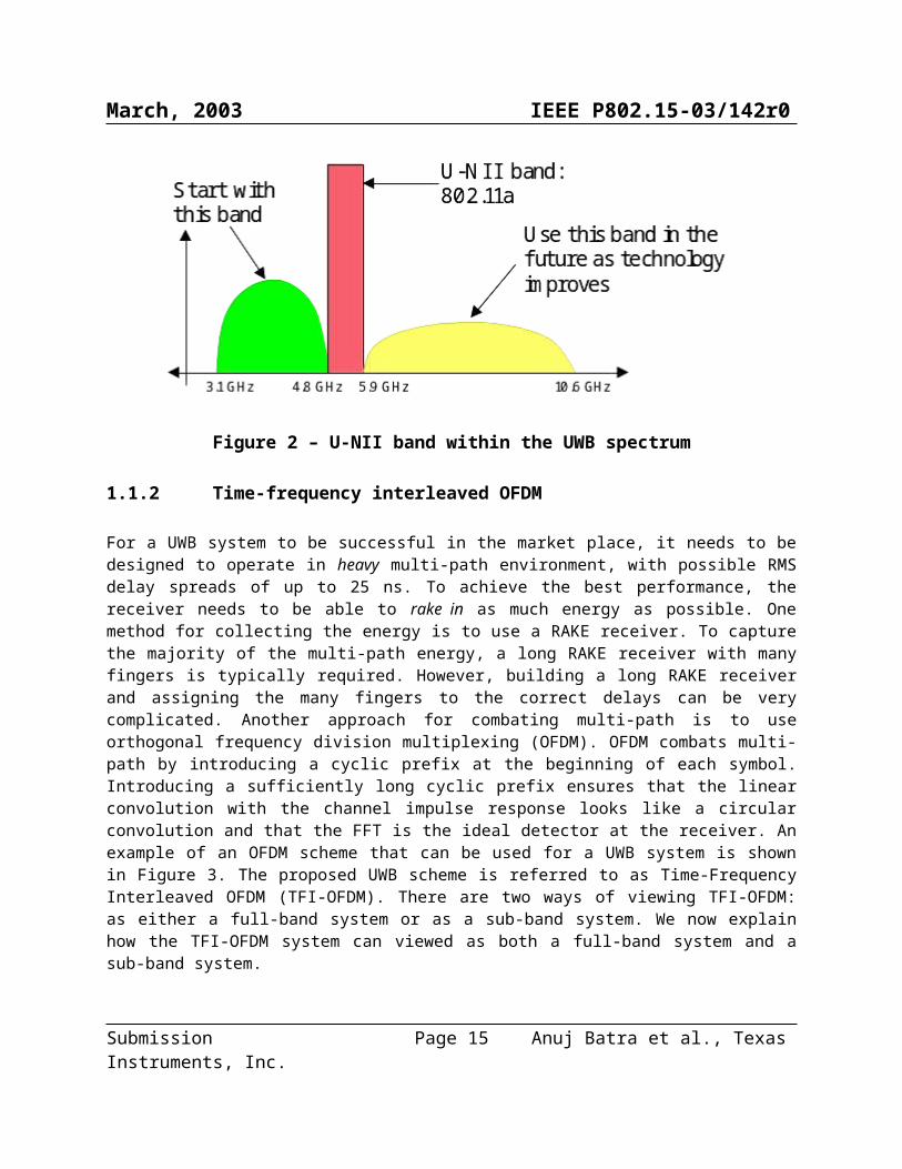
Another important criterion to keep in mind when selecting the operating bandwidth is that interferers may potentially lie within the band of interest. For example, in the United States, the U-NII band occupies the bandwidth from 5.15 GHz – 5.85 GHz, while in Japan, the U-NII band occupies the bandwidth from 4.9 GHz – 5.1 GHz. Both of these U-NII bands lie right in the middle of the allocated UWB spectrum (see Figure 2). If a UWB device uses an upper frequency that is larger than 6.0 GHz, then it will have to deal with the interference produced by IEEE 802.11a systems. It may be possible to mitigate, to some extent, this interference by using either static or adaptive notch filters or by using complicated baseband mitigation algorithms at the UWB receiver, but this mitigation will come at the expense of increased complexity. Conversely, the same UWB device will generate interference for IEEE 802.11a systems. To prevent generation of this interference, UWB devices will have to incorporate a notch filter at the transmitter to prevent emission within the U-NII band. Effectively, the presence of the U-NII band breaks the UWB spectrum into two distinct and orthogonal bands that are free from interference: 3.1 GHz – 4.8 GHz, and 6.0GHz – 10.6 GHz (see Figure 2).
Since the gains from using the higher band (6.0 GHz – 10.6 GHz) are incremental, we propose to use the lower band 3.1 – 4.8 GHz for the initial deployment of the proposed UWB system. Some other reasons for using the smaller operating bandwidth is that the front-end RF components, such as the LNA and mixer, can be built in current CMOS technologies with low noise figure; the signal processing can be done at lower speed, implying that the sampling rates for the ADC can be smaller, and the timing
Submission Page 8 Anuj Batra et al., Texas Instruments, Inc.
March, 2003 IEEE P802.15-03/142r0
requirement can be relaxed. As a result, the final solution will have lower complexity and can be manufactured using standard, and mature CMOS technologies, which implies an early time-to-market and low cost and low power solution.
In summary, the reasons for choosing the lower band for initial deployment are as follows:
Incremental gains from larger operating bandwidths, Lower sampling rates for the ADC, Relaxed timing requirements, Complete CMOS solutions for the proposed UWB system, Lower cost, Lower power, Early time-to-market, Scalability.
Even though the initial deployment will be centered around the lower band, the system will be designed in a scalable fashion, so that as the RF technology improves, the higher band can be added gracefully into the system.
Figure 2 – U-NII band within the UWB spectrum
1.1.2 Time-frequency interleaved OFDM
For a UWB system to be successful in the market place, it needs to be designed to operate in heavy multi-path environment, with possible RMS delay spreads of up to 25 ns. To achieve the best performance, the receiver needs to be able to rake in as much energy as possible. One method for collecting the energy is to use a RAKE receiver. To capture the majority of the multi-path energy, a long RAKE receiver with many fingers is typically required. However, building a long RAKE receiver and assigning the many fingers to the correct delays can be very complicated. Another approach for combating multi-path is to use orthogonal frequency division multiplexing (OFDM). OFDM combats multi-path by introducing a cyclic
Submission Page 9 Anuj Batra et al., Texas Instruments, Inc.
March, 2003 IEEE P802.15-03/142r0
prefix at the beginning of each symbol. Introducing a sufficiently long cyclic prefix ensures that the linear convolution with the channel impulse response looks like a circular convolution and that the FFT is the ideal detector at the receiver. An example of an OFDM scheme that can be used for a UWB system is shown in Figure 3. The proposed UWB scheme is referred to as Time-Frequency Interleaved OFDM (TFI-OFDM). There are two ways of viewing TFI-OFDM: as either a full-band system or as a sub-band system. We now explain how the TFI-OFDM system can viewed as both a full-band system and a sub-band system.
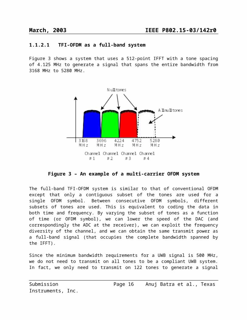
1.1.2.1 TFI-OFDM as a full-band system
Figure 3 shows a system that uses a 512-point IFFT with a tone spacing of 4.125 MHz to generate a signal that spans the entire bandwidth from 3168 MHz to 5280 MHz.
Figure 3 – An example of a multi-carrier OFDM system
The full-band TFI-OFDM system is similar to that of conventional OFDM except that only a contiguous subset of the tones are used for a single OFDM symbol. Between consecutive OFDM symbols, different subsets of tones are used. This is equivalent to coding the data in both time and frequency. By varying the subset of tones as a function of time (or OFDM symbol), we can lower the speed of the DAC (and correspondingly the ADC at the receiver), we can exploit the frequency diversity of the channel, and we can obtain the same transmit power as a full-band signal (that occupies the complete bandwidth spanned by the IFFT).
Since the minimum bandwidth requirements for a UWB signal is 500 MHz, we do not need to transmit on all tones to be a compliant UWB system. In fact, we only need to transmit on 122 tones to generate a signal that has a bandwidth greater than 500 MHz. To simplify the implementation, we can restrict our attention to subsets that contain a total of 128 consecutive tones. Therefore, the 512-point IFFT can be
Submission Page 10 Anuj Batra et al., Texas Instruments, Inc.
March, 2003 IEEE P802.15-03/142r0
divided into 4 non-overlapping sets of 128 tones. Since only 128 tones are used to generate a single OFDM symbol, the 512-point IFFT can be replaced by a much lower complexity 128-point IFFT.
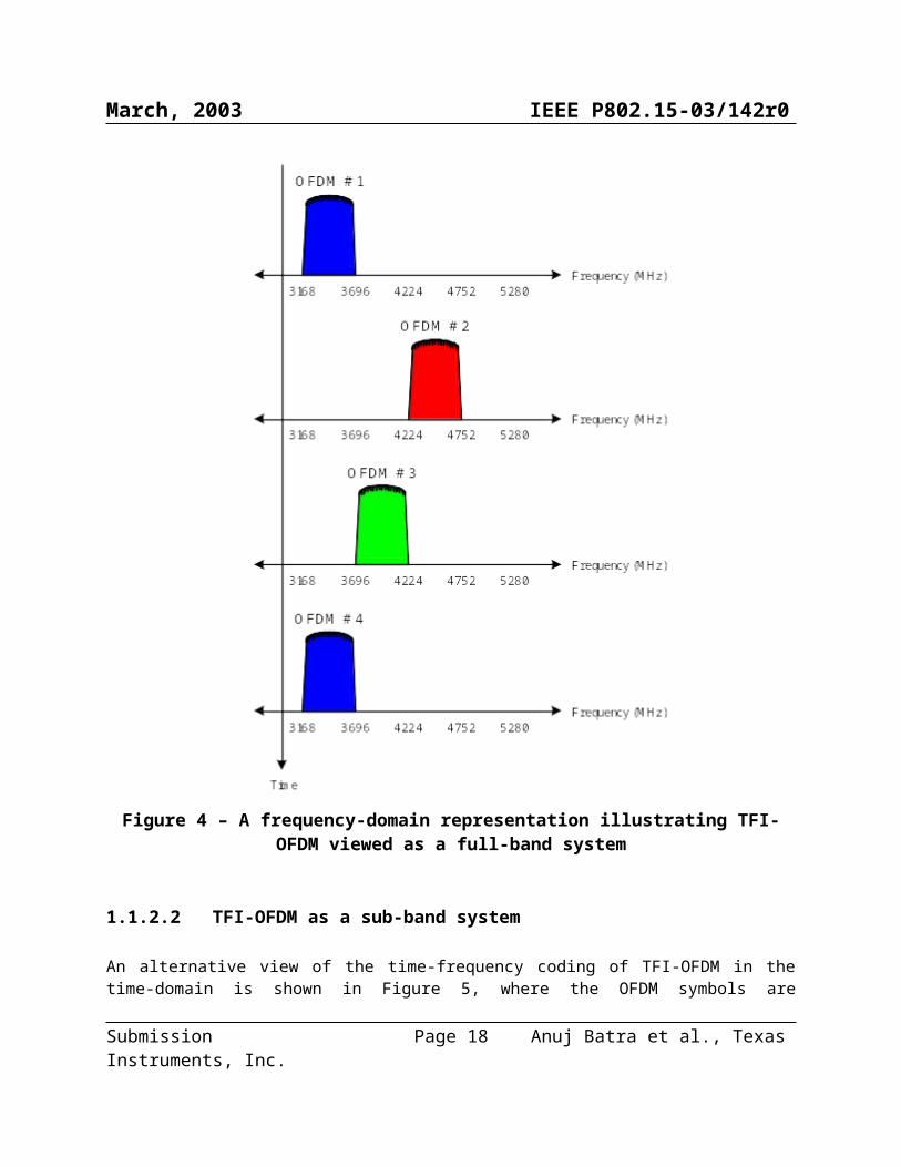
An example of how the data is transmitted on different subsets of tones is shown in Figure 4. In this example, data is transmitted in the first OFDM symbol on the first 128 tones (tones 1 through 128). For the second OFDM symbol, data is transmitted on tones 257 through 384 (third set of tones). For the third OFDM symbol, the data is transmitted on tones 129 through 256 (second set of tones). For the fourth OFDM symbol, the data is transmitted on the first 128 tones (tones 1 through 128), and so on. The period for this time-frequency coding pattern is three.
Submission Page 11 Anuj Batra et al., Texas Instruments, Inc.
March, 2003 IEEE P802.15-03/142r0
Figure 4 – A frequency-domain representation illustrating TFI-OFDM viewed as a full-band system
1.1.2.2 TFI-OFDM as a sub-band system
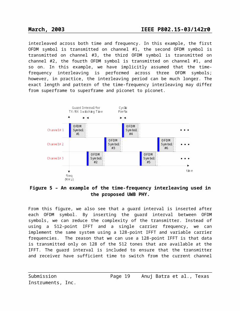
An alternative view of the time-frequency coding of TFI-OFDM in the time-domain is shown in Figure 5, where the OFDM symbols are interleaved across both time and frequency. In this example, the first OFDM symbol is transmitted on channel #1, the second OFDM symbol is transmitted on channel #3, the third OFDM symbol is transmitted on channel #2, the fourth OFDM symbol is transmitted on channel #1, and so on. In this example, we have implicitly assumed that the time-frequency interleaving is performed
Submission Page 12 Anuj Batra et al., Texas Instruments, Inc.
March, 2003 IEEE P802.15-03/142r0
across three OFDM symbols; however, in practice, the interleaving period can be much longer. The exact length and pattern of the time-frequency interleaving may differ from superframe to superframe and piconet to piconet.
Figure 5 – An example of the time-frequency interleaving used in the proposed UWB PHY.
From this figure, we also see that a guard interval is inserted after each OFDM symbol. By inserting the guard interval between OFDM symbols, we can reduce the complexity of the transmitter. Instead of using a 512-point IFFT and a single carrier frequency, we can implement the same system using a 128-point IFFT and variable carrier frequencies. The reason that we can use a 128-point IFFT is that data is transmitted only on 128 of the 512 tones that are available at the IFFT. The guard interval is included to ensure that the transmitter and receiver have sufficient time to switch from the current channel to the next channel. Thus, the TFI-OFDM system can be viewed as both a full-band UWB system and as a sub-band UWB system.
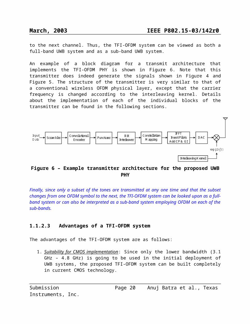
An example of a block diagram for a transmit architecture that implements the TFI-OFDM PHY is shown in Figure 6. Note that this transmitter does indeed generate the signals shown in Figure 4 and Figure 5. The structure of the transmitter is very similar to that of a conventional wireless OFDM physical layer, except that the carrier frequency is changed according to the interleaving kernel. Details about the implementation of each of the individual blocks of the transmitter can be found in the following sections.
Submission Page 13 Anuj Batra et al., Texas Instruments, Inc.
March, 2003 IEEE P802.15-03/142r0
Figure 6 – Example transmitter architecture for the proposed UWB PHY
Finally, since only a subset of the tones are transmitted at any one time and that the subset changes from one OFDM symbol to the next, the TFI-OFDM system can be looked upon as a full-band system or can also be interpreted as a sub-band system employing OFDM on each of the sub-bands.
1.1.2.3 Advantages of a TFI-OFDM system
The advantages of the TFI-OFDM system are as follows:
1. Suitability for CMOS implementation : Since only the lower bandwidth (3.1 GHz – 4.8 GHz) is going to be used in the initial deployment of UWB systems, the proposed TFI-OFDM system can be built completely in current CMOS technology.
2. U-NII interference suppression is easier : Since the TFI-OFDM system completely avoids all transmission in the U-NII band, the front-end filter design for rejecting interference from the U-NII band is simplified.
3. TFI-OFDM requires only one transmitter chain and one receiver chain : The guard interval ensures that only one transmit chain is needed to generate the TFI-OFDM waveform and that a single RF chain is sufficient to receive the transmitted signals at all times.
4. Early time-to-market : The majority of the TFI-OFDM system can be implemented in standard digital CMOS logic and because of the advantages stated above the analog implementation complexity can be minimized, which results in an early time-to-market.
5. Excellent robustness to multi-path: OFDM modulation has inherent robustness to multi-path channel environments and needs only a single-tap frequency-domain equalizer.
6. Compliance with worldwide regulations : Channels and individual tones can be dynamically turned on and off in order to comply with changing regulations.
7. Coexistence with future systems : Channels and individual tones can be dynamically turned on and off for enhanced coexistence with future systems.
Submission Page 14 Anuj Batra et al., Texas Instruments, Inc.
March, 2003 IEEE P802.15-03/142r0
8. Excellent robustness to narrow-band interference : OFDM modulation, which is the basis for TFI-OFDM, is inherently robust against single tone and narrowband interferers.
9. Antenna is easier to design : OFDM has an inherent robustness against gain, phase, and group delay variation that may be introduced by a broadband antenna.
1.1.3 Overview of the proposed UWB system description
1.1.3.1 Mathematical description of the signal
The transmitted signals can be described using a complex baseband signal notation. The actual RF transmitted signal is related to the complex baseband signal as follows:
,
where Re() represents the real part of a complex variable, rk(t) is the complex baseband signal of the kth
OFDM symbol and is nonzero over the interval from 0 to TSYM, N is the number of OFDM symbols, TSYM
is the symbol interval, and fk is the center frequency for the kth channel. The exact structure of the kth
OFDM symbol depends on its location within the packet:
.
The structure of each component of rk(t) as well as the offsets Npreamble, Nheader, and Ndata will be described in more detail in the following sections.
All of the OFDM symbols rk(t) can be constructed using an inverse Fourier transform with a certain set of coefficient Cn, where the coefficients are defined as either data, pilots, or training symbols:
.
The parameters f and NST are defined as the subcarrier frequency spacing and the number of total subcarriers used, respectively. The resulting waveform has a duration of TFFT = 1/f. Shifting the time by TCP creates the “circular prefix” which is used in OFDM to mitigate the effects of multipath. The parameter TGI is the guard interval duration.
Submission Page 15 Anuj Batra et al., Texas Instruments, Inc.
March, 2003 IEEE P802.15-03/142r0
The following description of the discrete time implementation is informational. The common way to implement the inverse Fourier transform is by an inverse Fast Fourier Transform (IFFT) algorithm. If, for example, a 128-point IFFT is used, the coefficients 1 to 61 are mapped to the same numbered IFFT inputs, while the coefficients –61 to –1 are copied into IFFT inputs 67 to 127. The rest of the inputs, 27 to 37 and the 0 (DC) input, are set to zero. This mapping is illustrated in Figure 7. After performing the IFFT, the output is cyclically extended and a guard interval is added to generate an output with the desired length.
Figure 7 – Input and outputs of IFFT
1.1.4 Scope
This subclause describes the PHY services provided to the IEEE 802.15.3 wireless PAN MAC. The OFDM PHY layer consists of two protocol functions, as follows:
a) A PHY convergence function, which adapts the capabilities of the physical medium dependent (PMD) system to the PHY service. This function is supported by the physical layer convergence procedure (PLCP), which defined a method of mapping the IEEE 802.11 PHY sublayer service data units (PSDU) into a framing format suitable for sending and receiving user data and management information between two or more stations using the associated PMD system.
Submission Page 16 Anuj Batra et al., Texas Instruments, Inc.
March, 2003 IEEE P802.15-03/142r0
b) A PMD system whose function defines the characteristics and method of transmitting and receiving data through a wireless medium between two or more stations, each using the OFDM system.
1.1.5 UWB PHY function
The UWB PHY contains three functional entities: the PMD function, the PHY convergence function, and the layer management function. The UWB PHY service is provided to the MAC through the PHY service primitives.
1.1.5.1 PLCP sublayer
In order to allow the IEEE 802.15.3 MAC to operate with minimum dependence on the PMD sublayer, a PHY convergence sublayer is defined. This function simplifies the PHY service interface to the IEEE 802.15.3 MAC services.
1.1.5.2 PMD sublayer
The PMD sublayer provides a means to send and receive data between two or more stations.
1.1.5.3 PHY management entity (PLME)
The PLME performs management of the local PHY functions in conjunction with the MAC management entity.
Submission Page 17 Anuj Batra et al., Texas Instruments, Inc.
March, 2003 IEEE P802.15-03/142r0
1.2 UWB PHY specific service parameter list
1.2.1 Introduction
Some PHY implementations require medium management state machines running in the MAC sublayer in order to meet certain PMD requirements. These PHY-dependent MAC state machines reside in a sublayer defined as the MAC sublayer management entity (MLME). In certain PMD implementations, the MLME may need to interact with the PLME as part of the normal PHY SAP primitives. These interactions are defined by the PLME parameter list currently defined in the PHY services primitives as TXVECTOR and RXVECTOR. The list of these parameters, and the values they may represent, are defined in the PHY specification for each PMD. This subclause addresses the TXVECTOR and RXVECTOR for the OFDM PHY.
1.2.2 TXVECTOR parameters
The parameters in Table 1 are defined as part of the TXVECTOR parameter list in the PHY-TXSTART.request service primitive.
55, 80, 110, 160, 200, 320, and 480(Support for 55, 110, and 200 data
rates is mandatory.)SCRAMBLER_INIT PHY-TXSTART.request
(TXVECTOR)Scrambler initialization: 2 null bits
TXPWR_LEVEL PHY-TXSTART.request(TXVECTOR)
1–8
1.2.2.1 TXVECTOR LENGTH
The allowed values for the LENGTH parameter are in the range 1–4095. This parameter is used to indicate the number of octets in the frame payload (which does not include the FCS), which the MAC is currently requesting the PHY to transmit. This value is used by the PHY to determine the number of octets transfers that will occur between the MAC and the PHY after receiving a request to start the transmission.
1.2.2.2 TXVECTOR DATARATE
Submission Page 18 Anuj Batra et al., Texas Instruments, Inc.
March, 2003 IEEE P802.15-03/142r0
The DATARATE parameter describes the bit rate at which the PLCP shall transmit the PSDU. Its value can be any of the rates defined in Table 1. Data rates of 55, 110, and 200 Mb/s shall be supported; other rates may also be supported.
1.2.2.3 TXVECTOR SCRAMBLER_INIT
The SCRAMBLER_INIT parameter consists of 2 null bits used for the scrambler initialization.
1.2.2.4 TXVECTOR TXPWR_LEVEL
The allowed values for the TXPWR_LEVEL parameter are in the range from 1–8. This parameter is used to indicate which of the available TxPowerLevel attributes defined in the MIB shall be used for the current transmission.
1.2.3 RXVECTOR parameters
The parameters in Table 2 are defined as part of the RXVECTOR parameter list in the PHY-RXSTART.indicate service primitive.
The allowed values for the LENGTH parameter are in the range 1–4095. This parameter is used to indicate the value contained in the LENGTH field that the PLCP has received in the PLCP header. The MAC and the PLCP will use this value to determine the number of octet transfers that will occur between the two sublayers during the transfer of the received PSDU.
1.2.3.2 RXVECTOR RSSI
The allowed values for the receive signal strength indicator (RSSI) parameter are in the range from 0 through RSSI maximum. This parameter is a measure by the PHY sublayer of the energy observed at the antenna used to receive the current PSDU. RSSI shall be measured during the reception of the PLCP preamble. RSSI is to be used in a relative manner, and it shall be a monotonically increasing function of the received power.
Submission Page 19 Anuj Batra et al., Texas Instruments, Inc.
March, 2003 IEEE P802.15-03/142r0
1.2.3.3 RXVECTOR DATARATE
DATARATE shall represent the data rate at which the current PPDU was received. The allowed values of the DATARATE are 55, 80, 110, 160, 200, 320, or 480.
Submission Page 20 Anuj Batra et al., Texas Instruments, Inc.
March, 2003 IEEE P802.15-03/142r0
1.3 UWB PLCP sublayer
1.3.1 Introduction
This subclause provides a method for converting the PSDUs to PPDUs. During the transmission, the PSDU shall be provided with a PLCP preamble and header to create the PPDU. At the receiver, the PLCP preamble and header are processed to aid in the demodulation, decoding, and delivery of the PSDU.
1.3.2 PLCP frame format
Figure 8 shows the format for the PHY frame including the PLCP preamble, PLCP and MAC headers, header check sequence, MAC frame body (frame payload plus FCS), tail bits, and pad bits. The PHY layer first pre-appends the PLCP header to the MAC header and then calculates the HCS over the combined PLCP and MAC headers. The resulting HCS is appended to the end of the MAC header. Tail bits are added to the MAC frame body (i.e., the frame payload plus FCS) in order to return the convolutional encoder to the “zero state”. If the size of the MAC frame body plus tail bits are not an integer multiple of the bits/OFDM symbol, then pad bits (PD) are added to the end of the tail bits in order to align the data stream on the OFDM symbol boundaries.
Figure 8 – PLCP frame format
The PLCP preamble is sent first, followed by the PLCP header, MAC header, and HCS, followed by the frame payload, the FCS, the tail bits, and finally the pad bits. As shown in Figure 8, the PLCP header, MAC header, and HCS are sent at an information data rate of 55 Mb/s. The remainder of the PLCP frame (frame payload, FCS, tail bits, and pad bits) is sent at the desired information data rate of 55, 80, 110, 160, 200, 320, or 480 Mb/s.
Submission Page 21 Anuj Batra et al., Texas Instruments, Inc.
March, 2003 IEEE P802.15-03/142r0
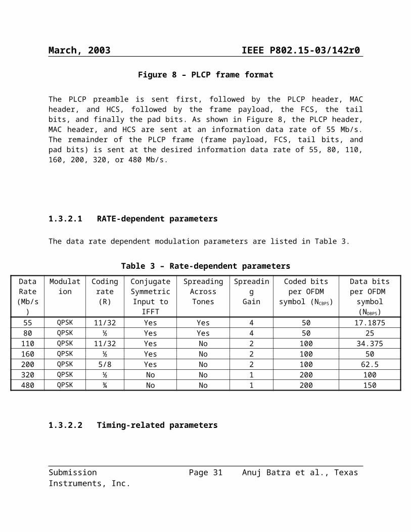
1.3.2.1 RATE-dependent parameters
The data rate dependent modulation parameters are listed in Table 3.
Table 3 – Rate-dependent parameters
Data Rate
(Mb/s)
Modulation
Coding rate(R)
ConjugateSymmetric
Input to IFFT
Spreading Across Tones
SpreadingGain
Coded bits per OFDM symbol
(NCBPS)
Data bits per OFDM
symbol (NDBPS)55 QPSK 11/32 Yes Yes 4 50 17.187580 QPSK ½ Yes Yes 4 50 25110 QPSK 11/32 Yes No 2 100 34.375160 QPSK ½ Yes No 2 100 50200 QPSK 5/8 Yes No 2 100 62.5320 QPSK ½ No No 1 200 100480 QPSK ¾ No No 1 200 150
1.3.2.2 Timing-related parameters
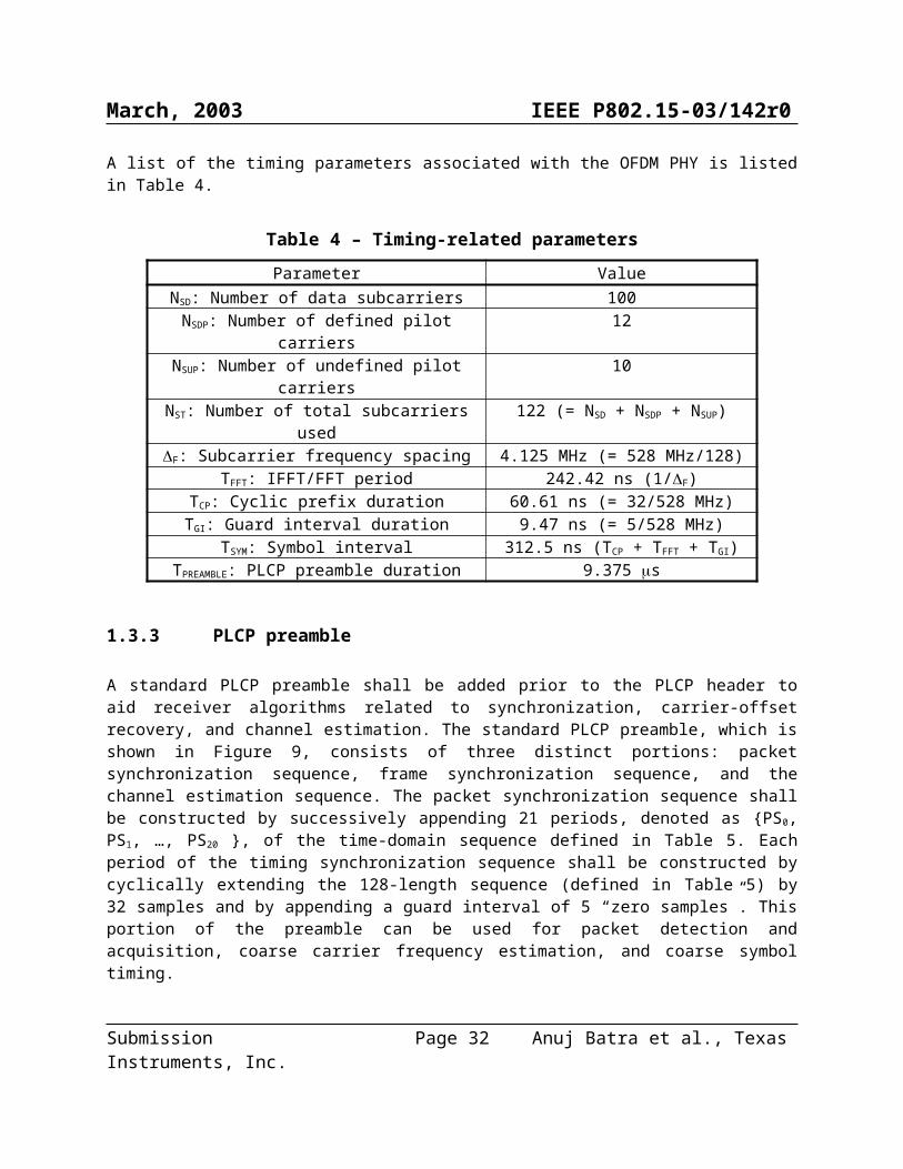
A list of the timing parameters associated with the OFDM PHY is listed in Table 4.
Table 4 – Timing-related parameters
Parameter ValueNSD: Number of data subcarriers 100
NSDP: Number of defined pilot carriers 12NSUP: Number of undefined pilot carriers 10
NST: Number of total subcarriers used 122 (= NSD + NSDP + NSUP) F: Subcarrier frequency spacing 4.125 MHz (= 528 MHz/128)
TSYM: Symbol interval 312.5 ns (TCP + TFFT + TGI)TPREAMBLE: PLCP preamble duration 9.375 s
1.3.3 PLCP preamble
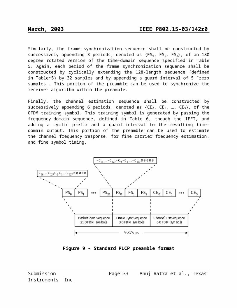
A standard PLCP preamble shall be added prior to the PLCP header to aid receiver algorithms related to synchronization, carrier-offset recovery, and channel estimation. The standard PLCP preamble, which is shown in Figure 9, consists of three distinct portions: packet synchronization sequence, frame synchronization sequence, and the channel estimation sequence. The packet synchronization sequence shall be constructed by successively appending 21 periods, denoted as {PS0, PS1, …, PS20 }, of the time-
Submission Page 22 Anuj Batra et al., Texas Instruments, Inc.
March, 2003 IEEE P802.15-03/142r0
domain sequence defined in Table 5. Each period of the timing synchronization sequence shall be constructed by cyclically extending the 128-length sequence (defined in Table 5) by 32 samples and by appending a guard interval of 5 “zero samples”. This portion of the preamble can be used for packet detection and acquisition, coarse carrier frequency estimation, and coarse symbol timing.
Similarly, the frame synchronization sequence shall be constructed by successively appending 3 periods, denoted as {FS0, FS1, FS2}, of an 180 degree rotated version of the time-domain sequence specified in Table 5. Again, each period of the frame synchronization sequence shall be constructed by cyclically extending the 128-length sequence (defined in Table 5) by 32 samples and by appending a guard interval of 5 “zero samples”. This portion of the preamble can be used to synchronize the receiver algorithm within the preamble.
Finally, the channel estimation sequence shall be constructed by successively appending 6 periods, denoted as {CE0, CE1, …, CE5}, of the OFDM training symbol. This training symbol is generated by passing the frequency-domain sequence, defined in Table 6, though the IFFT, and adding a cyclic prefix and a guard interval to the resulting time-domain output. This portion of the preamble can be used to estimate the channel frequency response, for fine carrier frequency estimation, and fine symbol timing.
Figure 9 – Standard PLCP preamble format
In addition to a standard PLCP preamble, a streaming-mode PLCP preamble is also defined in this section. In a streaming packet mode, the first packet shall use the standard PLCP preamble, while the remaining packets (second packet and on), which are separated by a MIFS time, shall use the streaming-mode PLCP preamble instead of the standard PLCP preamble. The streaming-mode PLCP preamble, which is shown in Figure 10, consists of three distinct portions: packet synchronization sequence, frame synchronization sequence, and the channel estimation sequence. The packet synchronization sequence
Submission Page 23 Anuj Batra et al., Texas Instruments, Inc.
March, 2003 IEEE P802.15-03/142r0
shall be constructed by successively appending 6 periods, denoted as {PS0, PS1, …, PS5 }, of the time-domain sequence defined in Table 5. Each period of the timing synchronization sequence shall be constructed by cyclically extending the 128-length sequence (defined in Table 5) by 32 samples and by appending a guard interval of 5 “zero samples”. This portion of the preamble can be used for packet detection and acquisition, coarse carrier frequency estimation, and coarse symbol timing.
Similarly, the frame synchronization sequence shall be constructed by successively appending 3 periods, denoted as {FS0, FS1, FS2}, of an 180 degree rotated version of the time-domain sequence specified in Table 5. Again, each period of the frame synchronization sequence shall be constructed by cyclically extending the 128-length sequence (defined in Table 5) by 32 samples and by appending a guard interval of 5 “zero samples”. This portion of the preamble can be used to synchronize the receiver algorithm within the preamble.
Finally, the channel estimation sequence shall be constructed by successively appending 6 periods, denoted as {CE0, CE1, …, CE5}, of the OFDM training symbol. This training symbol is generated by passing the frequency-domain sequence, defined in Table 6, though the IFFT, and adding a cyclic prefix and a guard interval to the resulting time-domain output. This portion of the preamble can be used to estimate the channel frequency response, for fine carrier frequency estimation, and fine symbol timing.
Figure 10 – Standard PLCP preamble format
Submission Page 24 Anuj Batra et al., Texas Instruments, Inc.
March, 2003 IEEE P802.15-03/142r0
Table 5 – Time-domain packet synchronization sequenceSequence Element
The PLCP header, MAC header, HCS, and tail bits shall be modulated using an information data rate of 55 Mb/s.
1.3.5 PLCP header
The OFDM training symbols shall be followed by the PLCP header, which contains the RATE of the MAC frame body, the length of the frame payload (which does not include the FCS), and the seed identifier for the data scrambler. The RATE field conveys the information about the type of modulation, the coding rate, and the spreading factor used to transmit the MAC frame body.
Submission Page 26 Anuj Batra et al., Texas Instruments, Inc.
March, 2003 IEEE P802.15-03/142r0
The PLCP header field shall be composed of 18 bits, as illustrated in Figure 11. The first three bits 0 to 2 shall encode the RATE. Bit 3 shall be reserved for future use. Bits 4–15 shall encode the LENGTH field, with the least significant bit (LSB) being transmitted first. Bits 16–17 shall encode the initial state of the scrambler, which is used to synchronize the descrambler of the receiver.
Figure 11 – PLCP Header bit assignment
1.3.5.1 Date rate (RATE)
Depending on the information data rate (RATE), the bits R1–R3 shall be set according to the values in Table 7.
Table 7 – Rate-dependent parameters
Rate (Mb/s) R1 – R3Reserved 110
55 01180 111110 001160 101200 010320 100480 000
The encoding of the RATE field values is chosen in such a way as to simplify the decoding process.
1.3.5.2 PLCP length field (LENGTH)
The PLCP Length field shall be an unsigned 12-bit integer that indicates the number of octets in the frame payload (which does not include the FCS, the tail bits, or the pad bits).
Submission Page 27 Anuj Batra et al., Texas Instruments, Inc.
March, 2003 IEEE P802.15-03/142r0
1.3.5.3 PLCP scrambler field (SCRAMBLER)
The bits S1–S2 shall be set according to the scrambler seed identifier value. This two-bit value corresponds to the seed value chosen for the data scrambler.
1.3.6 Data scrambler
A side-stream scrambler shall be used for the MAC header, HCS, and MAC frame body. The PLCP preamble, PLCP header, tail bits, and pad bits shall not be scrambled. The polynomial generator, g(D), for the pseudo random binary sequence (PRBS) generator shall be g(D) = 1 + D14 + D15, where D is a single bit delay element. The polynomial not only forms a maximal length sequence, but is also a primitive polynomial. Using this generator polynomial, the corresponding PRBS, xn, is generated as
where “” denotes modulo-2 addition. The following sequence defines the initialization sequence, xinit, which is specified by the parameter “seed value” in Table 8.
where represents the binary initial value at the output of the kth delay element.
The scrambled data bits, sn, are obtained as follows:
where bn represents the unscrambled data bits. The side-stream de-scrambler at the receiver shall be initialized with the same initialization vector, xinit, used in the transmitter scrambler. The initialization vector is determined from the seed identifier contained in the PLCP header of the received frame.
The 15-bit seed value shall correspond to the seed identifier as shown in Table 8. The seed identifier value is set to 00 when the PHY is initialized and is incremented in a 2-bit rollover counter for each frame that is sent by the PHY. The value of the seed identifier that is used for the frame is sent in the PLCP header.
Submission Page 28 Anuj Batra et al., Texas Instruments, Inc.
March, 2003 IEEE P802.15-03/142r0
The tail bit field shall be six bits of “0”, which are required to return the convolutional encoder to the “zero state”. This procedure improves the error probability of the convolutional decoder, which relies on the future bits when decoding the message stream. The tail bit field following the HCS shall be produced by replacing six “zero” bits following the end of the HCS with six non-scrambled “zero” bits. Similarly, the tail bit field following the MAC frame body shall be produced by replacing six “zero” bits following the end of the MAC frame body with six non-scrambled “zero” bits.
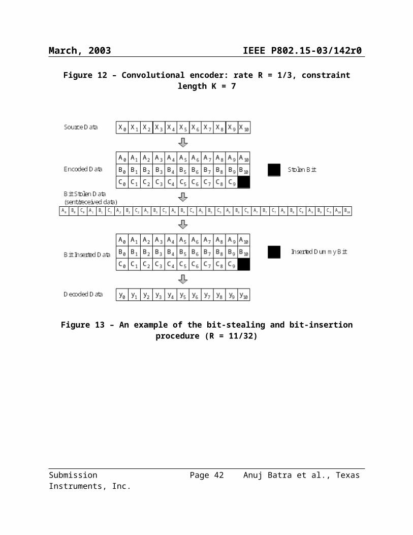
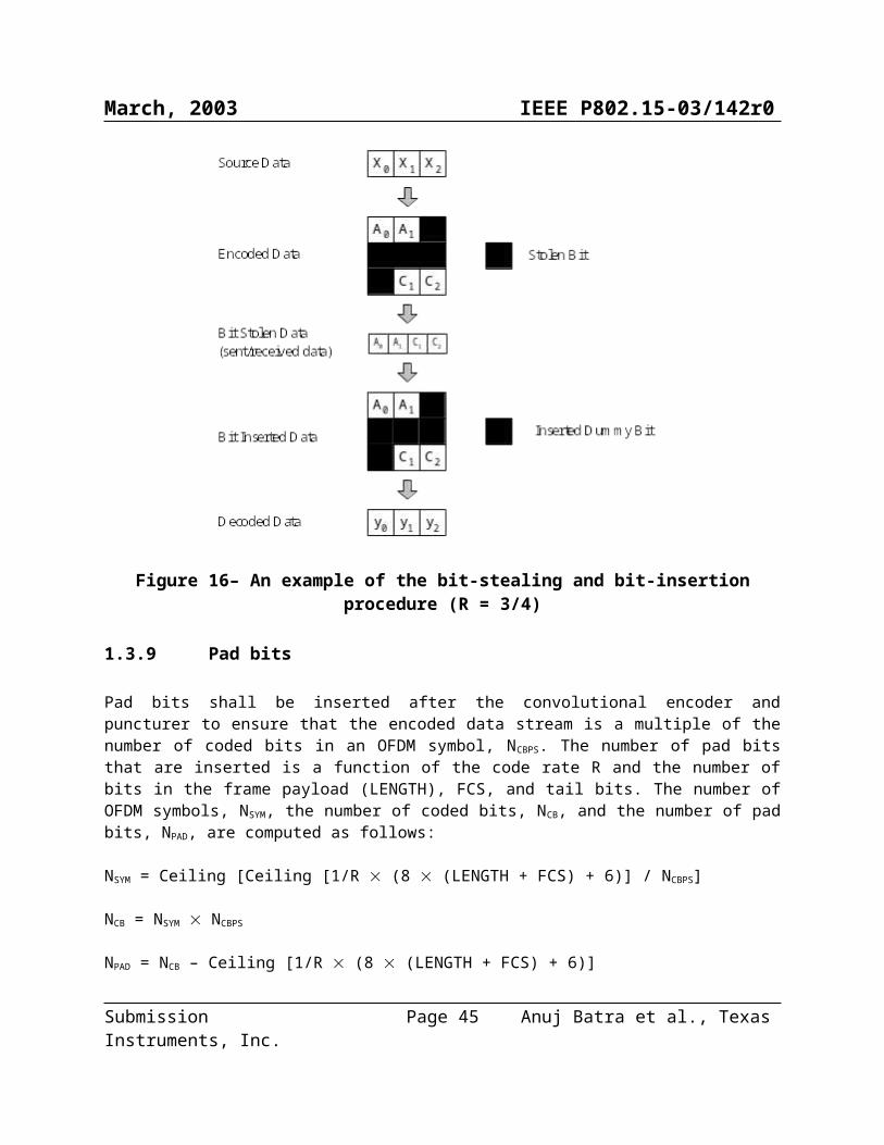
1.3.8 Convolutional Encoder
The PLCP header, MAC header, and HCS shall be coded with a convolutional encoder of rate R = 11/32. The MAC frame body and tail bits shall be coded with a convolutional encoder of rate R = 11/32, 1/2, 5/8, or 3/4, corresponding to the desired data rate. The convolutional encoder shall use the rate R = 1/3 industry-standard generator polynomials, g0 = 1338, g1 = 1458, and g2 = 1758, as shown in Figure 12. The bit denoted as “A” shall be the first bit generated by the encoder, followed by the bit denoted as “B”, and finally, by the bit denoted as “C”. The various coding rates are derived from the rate R = 1/3 convolutional code by employing “puncturing”. Puncturing is a procedure for omitting some of the encoded bits in the transmitter (thus reducing the number of transmitted bits and increasing the coding rate) and inserting a dummy “zero” metric into the convolutional decoder on the receive side in place of the omitted bits. The puncturing patterns are illustrated in Figure 13 through Figure 16.
Decoding by the Viterbi algorithm is recommended.
Figure 12 – Convolutional encoder: rate R = 1/3, constraint length K = 7
Submission Page 29 Anuj Batra et al., Texas Instruments, Inc.
March, 2003 IEEE P802.15-03/142r0
Figure 13 – An example of the bit-stealing and bit-insertion procedure (R = 11/32)
Submission Page 30 Anuj Batra et al., Texas Instruments, Inc.
March, 2003 IEEE P802.15-03/142r0
Figure 14 – An example of the bit-stealing and bit-insertion procedure (R = 1/2)
Submission Page 31 Anuj Batra et al., Texas Instruments, Inc.
March, 2003 IEEE P802.15-03/142r0
Figure 15 – An example of the bit-stealing and bit-insertion procedure (R = 5/8)
Submission Page 32 Anuj Batra et al., Texas Instruments, Inc.
March, 2003 IEEE P802.15-03/142r0
Figure 16– An example of the bit-stealing and bit-insertion procedure (R = 3/4)
1.3.9 Pad bits
Pad bits shall be inserted after the convolutional encoder and puncturer to ensure that the encoded data stream is a multiple of the number of coded bits in an OFDM symbol, NCBPS. The number of pad bits that are inserted is a function of the code rate R and the number of bits in the frame payload (LENGTH), FCS, and tail bits. The number of OFDM symbols, NSYM, the number of coded bits, NCB, and the number of pad bits, NPAD, are computed as follows:
The function Ceiling () is a function that returns the smallest integer value greater than or equal to its argument value. The appended bits (“pad bits”) are set to “zeros” and are subsequently scrambled with the rest of the bits in the MAC frame payload.
Submission Page 33 Anuj Batra et al., Texas Instruments, Inc.
March, 2003 IEEE P802.15-03/142r0
1.3.10 Bit interleaving
The coded bit stream is interleaved prior to modulation. Bit interleaving provides robustness against burst errors. The bit interleaving operation is performed in two stages: symbol interleaving followed by tone interleaving. The symbol interleaver permutes the bits across OFDM symbols to exploit frequency diversity across the sub-bands, while the tone interleaver permutes the bits across the data tones within an OFDM symbol to exploit frequency diversity across tones and provide robustness against narrow-band interferers. We constrain our symbol interleaver to interleave among at most three consecutive OFDM symbols. This corresponds to a maximum interleaving latency of slightly less than 1 s.
Let NCBPS be the number of coded bits per OFDM symbol. First, the coded bits are grouped together into blocks of 3NCBPS coded bits, which corresponds to three OFDM symbols. Each group of coded bits is then permuted using a regular symbol block interleaver of size NCBPS 3.Let the sequences {U(i)} and {S(j)}, where i, j = 0,…, 3NCBPS1, represent the input and output bits of the symbol block interleaver, respectively. The input-output relationship of this interleaver is given by:
,
where the function Floor() returns the largest integer value less than or equal to its argument value and where the function Mod() returns the remainder after division of NCBPS by i. If the coded bits available at the input of the symbol block interleaver correspond to less than three OFDM symbols, then the symbol interleaving operation is not performed on these bits. This condition is expected to occur towards the end of the packet, when the number of coded bits available to the symbol block interleaver only corresponds to that of 1 or 2 OFDM symbols.
The output of the symbol block interleaver is then passed through a tone block interleaver. The outputs of the symbol block interleaver after grouped together into blocks of NCBPS bits and then permuted using a regular block interleaver of size NTint 10, where NTint = NCBPS/10. Let the sequences {S(i)} and {V(j)}, where i, j = 0,…, NCBPS1, represent the input and output bits of the tone interleaver, respectively. The input-output relationship of the tone block interleaver is given by:
,
where the function Mod() returns the remainder after division of NTint by i.
1.3.11 Subcarrier constellation mapping
The OFDM subcarriers shall be modulated using either BPSK or QPSK modulation. The encoded and interleaved binary serial input data shall be divided into groups of 1 or 2 bits and converted into complex numbers representing BPSK or QPSK constellation points. The conversion shall be performed according to the Gray-coded constellation mappings, illustrated in Figure 17, with the input bit, b0, being the earliest
Submission Page 34 Anuj Batra et al., Texas Instruments, Inc.
March, 2003 IEEE P802.15-03/142r0
in the stream. The output values, d, are formed by multiplying the resulting (I + jQ) value by a normalization factor of KMOD, as described in the following equation:
d = (I + jQ) KMOD.
The normalization factor, KMOD, depends on the base modulation mode, as prescribed in Table 9. Note that the modulation type can be different form the start to end of the transmission, as the signal changes from the channel estimation sequence to the MAC frame body. The purpose of the normalization factor is to achieve the same average power for all mappings. In practical implementations, an approximate value of the normalization factor can be used, as long as the device conforms to the modulation accuracy requirements.
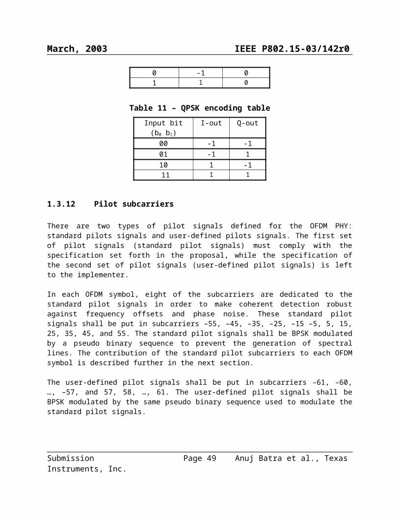
For BPSK, b0 determines the I value, as illustrated in Table 10. For QPSK, b0 determines the I value and b1 determines the Q value, as illustrated in Table 11.
Figure 17 – BPSK and QPSK constellation bit encoding
There are two types of pilot signals defined for the OFDM PHY: standard pilots signals and user-defined pilots signals. The first set of pilot signals (standard pilot signals) must comply with the specification set forth in the proposal, while the specification of the second set of pilot signals (user-defined pilot signals) is left to the implementer.
In each OFDM symbol, eight of the subcarriers are dedicated to the standard pilot signals in order to make coherent detection robust against frequency offsets and phase noise. These standard pilot signals shall be put in subcarriers –55, –45, –35, –25, –15 –5, 5, 15, 25, 35, 45, and 55. The standard pilot signals shall be BPSK modulated by a pseudo binary sequence to prevent the generation of spectral lines. The contribution of the standard pilot subcarriers to each OFDM symbol is described further in the next section.
The user-defined pilot signals shall be put in subcarriers –61, –60, …, –57, and 57, 58, …, 61. The user-defined pilot signals shall be BPSK modulated by the same pseudo binary sequence used to modulate the standard pilot signals.
1.3.13 OFDM modulation
For information data rates of 55 and 80 Mb/s, the stream of complex numbers is divided into groups of 25 complex numbers. We shall denote these complex numbers cn,k, which corresponds to subcarrier n of OFDM symbol k, as follows:
where NSYM denotes the number of OFDM symbols in the MAC frame body, tail bits, and pad bits.
For information data rates of 110, 160, and 200 Mb/s, the stream of complex numbers is divided into groups of 50 complex numbers. We shall denote these complex numbers cn,k, which corresponds to subcarrier n of OFDM symbol k, as follows:
Submission Page 36 Anuj Batra et al., Texas Instruments, Inc.
March, 2003 IEEE P802.15-03/142r0
where NSYM denotes the number of OFDM symbols in the MAC frame body, tail bits, and pad bits.
For information data rates of 320 and 480 Mb/s, the stream of complex numbers is divided into groups of 100 complex numbers. We shall denote these complex numbers cn,k, which corresponds to subcarrier n of OFDM symbol k, as follows:
where NSYM denotes the number of OFDM symbols in the MAC frame body, tail bits, and pad bits.
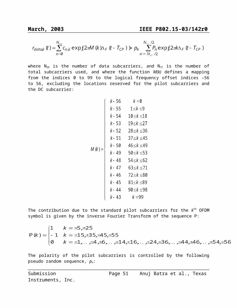
An OFDM symbol rdata,k(t) is defined as
where NSD is the number of data subcarriers, and NST is the number of total subcarriers used, and where the function M(k) defines a mapping from the indices 0 to 99 to the logical frequency offset indices –56 to 56, excluding the locations reserved for the pilot subcarriers and the DC subcarrier:
The contribution due to the standard pilot subcarriers for the kth OFDM symbol is given by the inverse Fourier Transform of the sequence P:
Submission Page 37 Anuj Batra et al., Texas Instruments, Inc.
March, 2003 IEEE P802.15-03/142r0
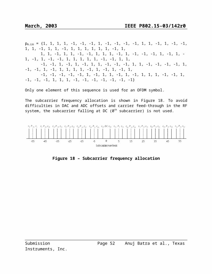
The polarity of the pilot subcarriers is controlled by the following pseudo random sequence, pn:
Only one element of this sequence is used for an OFDM symbol.
The subcarrier frequency allocation is shown in Figure 18. To avoid difficulties in DAC and ADC offsets and carrier feed-through in the RF system, the subcarrier falling at DC (0 th subcarrier) is not used.
Figure 18 – Subcarrier frequency allocation
Submission Page 38 Anuj Batra et al., Texas Instruments, Inc.
March, 2003 IEEE P802.15-03/142r0
1.4 General requirements
1.4.1 Operating channel frequencies
1.4.1.1 Operating frequency range
This PHY operates in the 3.1 – 10.6 GHz frequency as regulated in the United States by the Code of Federal Regulations, Title 47, Section 15, as well as in any other areas that the regulatory bodies have also allocated this band.
1.4.1.2 Channel numbering
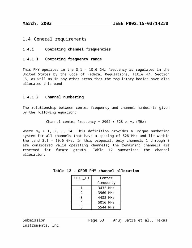
The relationship between center frequency and channel number is given by the following equation:
Channel center frequency = 2904 + 528 nch (MHz)
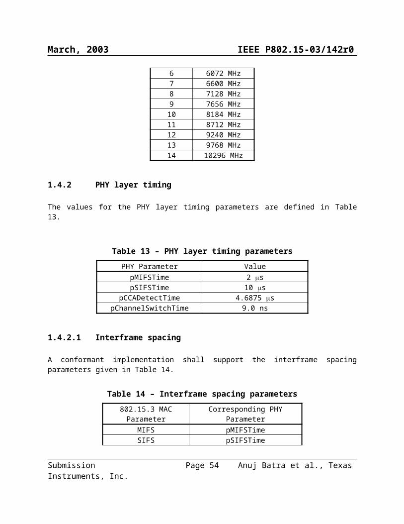
where nch = 1, 2, …, 14. This definition provides a unique numbering system for all channels that have a spacing of 528 MHz and lie within the band 3.1 – 10.6 GHz. In this proposal, only channels 1 through 3 are considered valid operating channels; the remaining channels are reserved for future growth. Table 12 summarizes the channel allocation.
The RX-to-TX turnaround time shall be pSIFSTime. This turnaround time shall be measured at the air interface from the trailing edge of the last received OFDM symbol to the leading edge of the first transmitted OFDM symbol of the PLCP preamble for the next frame.
1.4.2.3 Transmit-to-receive turnaround time
The TX-to-RX turnaround time shall be pSIFSTime. This turnaround time shall be measured at the air interface from the trailing edge of the last transmitted symbol until the receiver is ready to begin the reception of the next PHY frame.
1.4.2.4 Time between successive transmissions
Submission Page 40 Anuj Batra et al., Texas Instruments, Inc.
March, 2003 IEEE P802.15-03/142r0
The time between uninterrupted successive transmissions by the same DEV shall be pMIFSTime. This time shall be measured at the air interface from the trailing edge of the last OFDM symbol transmitted to the leading edge of the first OFDM symbol of the PLCP preamble for the following frame.
1.4.2.5 Channel switch time
The channel switch time is defined as the interval from when the trailing edge of the last valid OFDM symbol is on air until the PHY is ready to transmit or receive from the air another OFDM symbol on a new channel. The channel switch time shall not exceed pChannelSwitchTime.
1.4.3 Header check sequence
The combined PLCP and MAC headers shall be protected with a CCITT CRC-16 header check sequence (HCS). The PHY parameter, pLengthHCS shall be 2 for this PHY. The CCITT CRC-16 HCS shall be the ones complement of the remainder generated by the modulo-2 division of the protected combined PLCP and MAC headers by the polynomial: . The protected bits shall be processed in the transmit order. All HCS calculations shall be made prior to data scrambling. A schematic of the processing order is shown in Figure 19.
Figure 19 – CCITT CRC-16 Implementation
The CRC-16 described in this subclause is the same one used in the IEEE 802.15.3 draft standard.
Submission Page 41 Anuj Batra et al., Texas Instruments, Inc.
March, 2003 IEEE P802.15-03/142r0
1.5 Transmitter specifications
1.5.1 Transmit PSD mask
The transmitted spectrum shall have a 0 dBr (dB relative to the maximum spectral density of the signal) bandwidth not exceeding 260 MHz, –12 dBr at 285 MHz frequency offset, and –20 dBr at 330 MHz frequency offset and above. The transmitted spectral density of the transmitted signal mask shall fall within the spectral, as shown in Figure 20.
Figure 20 – Transmit Power Spectral Density Mask
1.5.2 Transmit center frequency tolerance
The transmitted center frequency tolerance shall be 20 ppm maximum.
1.5.3 Symbol clock frequency tolerance
The symbol clock frequency tolerance shall be 20 ppm maximum.
1.5.4 Clock synchronization
The transmit center frequency and the symbol clock frequency shall be derived from the same reference oscillator.
Submission Page 42 Anuj Batra et al., Texas Instruments, Inc.
March, 2003 IEEE P802.15-03/142r0
1.6 Receiver specification
1.6.1 Receiver sensitivity
For a packet error rate (PER) of less than 8% with a PSDU of 1024 bytes, the minimum receiver sensitivity numbers for the various rates are listed in Table 15.
The start of a valid OFDM transmission at a receiver level equal to or greater than the minimum 55 Mb/s sensitivity (83 dBm) shall cause CCA to indicate busy with a probability > 90% within 4.6875 s. If the preamble portion was missed, the receiver shall hold the carrier sense (CS) signal busy for any signal 20 dB above the minimum 55 Mb/s sensitivity (63 dBm).
Submission Page 43 Anuj Batra et al., Texas Instruments, Inc.
March, 2003 IEEE P802.15-03/142r0
2 Self evaluation matrix
2.1 General solution criteria
REF. IMPORTANCELEVEL PROPOSER RESPONSE
Unit Manufacturing Complexity (UMC)
3.1B +
Signal RobustnessInterference And Susceptibility 3.2.2
A+
Coexistence 3.2.3 A +
Technical Feasibility
Manufacturability 3.3.1 A +
Time To Market 3.3.2 A +
Regulatory Impact 3.3.3 A +
Scalability (i.e. Payload Bit Rate/Data Throughput, Channelization – physical or coded, Complexity, Range, Frequencies of Operation, Bandwidth of Operation, Power Consumption)
3.4 A
+
Location Awareness 3.5 C 0
Submission Page 44 Anuj Batra et al., Texas Instruments, Inc.
March, 2003 IEEE P802.15-03/142r0
2.2 PHY protocol criteria
CRITERIA REF. IMPORTANCE LEVEL PROPOSER RESPONSE
Size And Form Factor 5.1B
+
PHY-SAP Payload Bit Rate & Data ThroughputPayload Bit Rate 5.2.1
A+
Packet Overhead 5.2.2 A +
PHY-SAP Throughput 5.2.3 A +
Simultaneously Operating Piconets
5.3 A +
Signal Acquisition 5.4 A +
System Performance 5.5 A +
Link Budget 5.6 A +
Sensitivity 5.7 A +
Power Management Modes 5.8 B +
Power Consumption 5.9 A +
Antenna Practicality 5.10 B +
Submission Page 45 Anuj Batra et al., Texas Instruments, Inc.
March, 2003 IEEE P802.15-03/142r0
2.3 MAC protocol enhancement criteria
CRITERIA REF. IMPORTANCE LEVEL PROPOSER RESPONSE
MAC Enhancements And Modifications
4.1.C +
Submission Page 46 Anuj Batra et al., Texas Instruments, Inc.
March, 2003 IEEE P802.15-03/142r0
3 Detailed responses to selection criteria and self-evaluation matrix
3.1 Unit manufacturing cost
The total die size for the PHY solution is expected to be around 4.2 mm2, with 2.7 mm2 for the analog/RF portion and 1.5 mm2 for the digital portion. These estimates assume a 90 nm CMOS technology node in 2005. The digital portion of the PHY is expected to require 295K gates. The enhancements to the MAC are not expected to affect the die size or gate count of the MAC. The major external components that will be required by the complete solution (RF+PHY+MAC) are a pre-select filter, balun, crystal oscillator, voltage regulator, and SRAM for the MAC.
3.2 Signal robustness
3.2.2 Interference and susceptibility
The receiver consists of a front-end pre-select filter to reject out-of band noise and interference. For the three-band TFI-OFDM system presented in this proposal, the pass-band of the pre-select filter is between 3168 MHz to 4752 MHz. The output of the pre-select filter is amplified using an LNA and is followed by down-conversion to the base-band using the appropriate center frequency. The base-band signal is filtered using a 3rd order low-pass filter.
For the interference and susceptibility analysis, the proposed UWB system is assumed to be operating at 6 dB above the receiver sensitivity, namely Pd = –74 dBm (see Table 24), for an information data rate of 110 Mbps. Based on the link budget table of section Error: Reference source not found, the average noise power per bit is –87 dBm. Since, a margin of 6 dB is available, the sum of the interferer-and-noise power can be at most –81 dBm to maintain a PER < 8% for a 1024 byte packet. Under the assumption that the impact of the interferer is similar to that of additive noise, this corresponds to a maximum tolerable interferer power of –82.3 dBm at the input of the decoder. The interference and susceptibility analysis for the following types of interferers has been provided in Table 16:
Microwave oven
IEEE 802.15.1 (Bluetooth)
IEEE 802.11b
IEEE 802.15.3
IEEE 802.11a
IEEE 802.15.4
Table 16 – Interference and Susceptibility Analysis
Submission Page 47 Anuj Batra et al., Texas Instruments, Inc.
March, 2003 IEEE P802.15-03/142r0
Microwave Oven
Bluetooth & IEEE 802.15.1
Interferer
IEEE 802.11b & IEEE 802.15.3
Interferer
IEEE 802.11a Interferer
IEEE 802.15.4 Interferer
(2.45 GHz)Max. tolerable interferer
power at the encoder -82.3 dBm -82.3 dBm -82.3 dBm -82.3 dBm -82.3 dBm
Processing gain (coding rate of 11/32) 4.6 dB 4.6 dB 4.6 dB 4.6 dB 4.6 dB
Minimum base-band filter attenuation 35.4 dB 36.9 dB 36.9 dB 30.7 dB 35.6 dB
Front-end pre-select filter attenuation 35 dB 35 dB 35 dB 30 dB 35 dB
Max. tolerable interferer power at the antenna -7.3 dB -5.8 dB -5.8 dB -17 dB -7.1 dB
Interferer power at 1m separation -23.2 dBm -40 dBm -20 dBm -31.9 dBm -40.2 dBm
Minimum margin 15.9 dB 34.2 dB 14.2 dB 14.1 dB 33.1 dBTolerable separation 0.16 m 0.02 m 0.2 m 0.2 m 0.02 m
3.2.2.1 Microwave oven
The microwave oven is an out-of-band interferer and based on the analysis presented in Table 16, the TFI-OFDM system can tolerate this interferer at a minimum separation of 0.16 m.
3.2.2.2 Bluetooth and IEEE 802.15.1 interferer
This is an out-of-band interferer and based on the analysis presented in Table 16, the TFI-OFDM system can tolerate this interferer at a minimum separation of 0.02 m.
3.2.2.3 IEEE 802.11b and IEEE 802.15.3 interferer
This is an out-of-band interferer and based on the analysis presented in Table 16, the TFI-OFDM system can tolerate this interferer at a minimum separation of 0.2 m. This interference tolerance is superior to the desired criteria of 0.3 m separation between the IEEE 802.11b interferer and the UWB reference device.
3.2.2.4 IEEE 802.11a interferer
As the TFI-OFDM system only utilizes the spectrum between 3168 MHz and 4752 MHz, the IEEE 802.11a interferer is an out-of-band interferer. Hence, it is easier to design the front-end pre-select filter to reject the 802.11a interference. Based on the analysis presented in Table 16, the TFI-OFDM system can tolerate this interferer at a minimum separation of at least 0.2 m. This interference tolerance is superior to the desired criteria of 0.3 m separation between the IEEE 802.11a interferer and the UWB reference device.
3.2.2.5 IEEE 802.15.4 interferer
Submission Page 48 Anuj Batra et al., Texas Instruments, Inc.
March, 2003 IEEE P802.15-03/142r0
This is an out-of-band interferer and the TFI-OFDM system can tolerate this interferer at a minimum separation of 0.02 m. The analysis presented in Table 16 is only for the IEEE 802.15.4 interferer centered around 2.45 GHz. Although, the 802.15.4 device centered around 868 MHz and 915 MHz can have a receive power that is approximately 9 dB higher than that of the 802.15.4 device centered around 2.45 GHz, the base-band filter attenuation for these frequencies is significantly higher, and hence the 802.15.4 device with a center frequency of 2.45 GHz is the worst-case interferer.
3.2.2.6 Generic in-band modulated interferer
The robustness of the TFI-OFDM system to the presence of a generic in-band modulated interferer was evaluated based on simulations. Since the symbol rate of the modulated interferer is only 5 MHz, it will interfere with only a couple of tones. The affected tones can be erased to combat the narrow-band interferer and erasure of these tones results in some performance degradation. One of the advantages of the TFI-OFDM system is that the sub-band in which the narrow band interferer is present can still be used with minimal impact. When operating at 6 dB above sensitivity, it was observed that for the worst case location of the interferer center frequency, the TFI-OFDM system can tolerate a generic in-band modulated interferer with a power of PI > Pd – 3.8 dB.
3.2.2.7 Generic in-band tone interferer
The robustness of the TFI-OFDM system to the presence of a generic in-band tone interferer was evaluated based on simulations. A generic in-band tone interferer will affect at most two tones in any OFDM symbol. The affected tones can be erased to combat the narrow-band interferer and erasure of these tones results in some performance degradation. Hence, the sub-band in which the narrow band interferer is present can still be used with minimal impact. When operating at 6 dB above sensitivity, it was observed that for the worst case location of the interferer center frequency, the TFI-OFDM system can tolerate a generic in-band tone interferer with a power of PI > Pd – 4.8 dB.
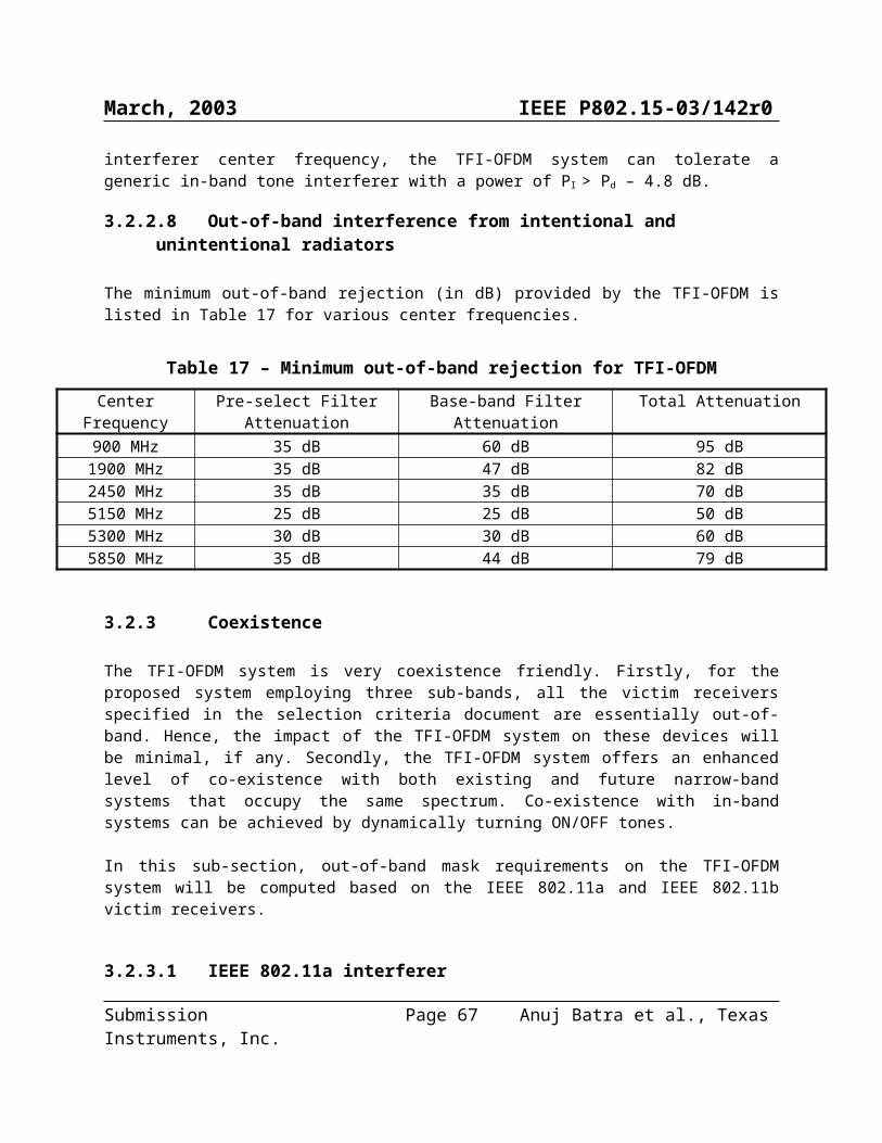
3.2.2.8 Out-of-band interference from intentional and unintentional radiators
The minimum out-of-band rejection (in dB) provided by the TFI-OFDM is listed in Table 17 for various center frequencies.
Table 17 – Minimum out-of-band rejection for TFI-OFDM
Center Frequency Pre-select Filter Attenuation Base-band Filter Attenuation Total Attenuation900 MHz 35 dB 60 dB 95 dB
1900 MHz 35 dB 47 dB 82 dB2450 MHz 35 dB 35 dB 70 dB5150 MHz 25 dB 25 dB 50 dB5300 MHz 30 dB 30 dB 60 dB5850 MHz 35 dB 44 dB 79 dB
Submission Page 49 Anuj Batra et al., Texas Instruments, Inc.
March, 2003 IEEE P802.15-03/142r0
3.2.3 Coexistence
The TFI-OFDM system is very coexistence friendly. Firstly, for the proposed system employing three sub-bands, all the victim receivers specified in the selection criteria document are essentially out-of-band. Hence, the impact of the TFI-OFDM system on these devices will be minimal, if any. Secondly, the TFI-OFDM system offers an enhanced level of co-existence with both existing and future narrow-band systems that occupy the same spectrum. Co-existence with in-band systems can be achieved by dynamically turning ON/OFF tones.
In this sub-section, out-of-band mask requirements on the TFI-OFDM system will be computed based on the IEEE 802.11a and IEEE 802.11b victim receivers.
3.2.3.1 IEEE 802.11a interferer
The IEEE 802.11a receiver has a minimum receiver sensitivity of –82 dBm and a signal bandwidth of 20 MHz. For the average interfering power of the UWB device to be at least 6 dB less than the minimum sensitivity level of the victim receiver, at a distance separation of 0.3 m, the transmit power of the UWB device in the bandwidth of interest should be less than –51.5 dBm or equivalently –64.5 dBm/MHz. This corresponds to an out-of-band rejection mask of at least 23 dB at a frequency of 5.3 GHz. This level of out-of-band rejection can be easily achieved at the transmitter by using the front-end pre-select filter
3.2.3.2 IEEE 802.11b interferer
The IEEE 802.11b receiver has a minimum receiver sensitivity of –76 dBm and a signal bandwidth of 11 MHz. For the average interfering power of the UWB device to be at least 6 dB less than the minimum sensitivity level of the victim receiver, at a distance separation of 0.3 m, the transmit power of the UWB device in the bandwidth of interest should be less than –52.4 dBm or equivalently –62.8 dBm/MHz. This corresponds to an out-of-band rejection mask of at least 22 dB at a frequency of 2.4 GHz. This level of out-of-band rejection can be easily achieved at the transmitter by using the front-end pre-select filter.
3.3 Technical feasibility
3.3.1 Manufacturability
The proposed UWB solution will leverage current standard CMOS technology. Leveraging the standard analog and digital CMOS technology will result in a straightforward development effort. In addition, the digital section of the proposed PHY is similar to that of conventional and mature OFDM solutions, such as 802.11a and 802.11g.
3.3.2 Time to market
he earliest a complete CMOS PHY solution would be ready for integration is 2005.
Submission Page 50 Anuj Batra et al., Texas Instruments, Inc.
March, 2003 IEEE P802.15-03/142r0
3.3.3 Regulatory impact
The proposed PHY complies the rules specified in the United States Code of Federal Regulations, Title 47, Section 15, Parts 15.517, 15.519, and 15.521 The proposed scheme will also comply in regions where they adopt the ruling specified by the FCC. Currently, there are no standardized regulations for UWB technologies in Europe, Japan, and Korea. However, regulatory efforts are underway in these regions. Due to the flexibility of the proposed scheme, it will comply with most regulatory standards.
3.4 Scalability
The proposed system demonstrates scalability of the following parameters:
1. Power Consumption: The power consumption scales monotonically with information data rate. The power consumption values are listed as a function of the information data rates in Table 25.
2. Payload Bit Rate and Throughput: Several payload bit rates have been specified for the TFI-OFDM system in Table 3. Additional payload bit rates can be incorporated in the proposed system by defining new spreading/coding rates. New coding rates can be obtained by puncturing the rate 1/3 mother code and defining new puncturing patterns.
3. Channelization: Fourteen non-overlapping physical channels have been defined for the TFI-OFDM system in Table 12. In the initial system, three channels will be used and more channels can be added as the RF technology improves.
4. Complexity: The system complexity monotonically scales with the information data rate.
5. Range: The range of the TFI-OFDM system is a function of the data rate of operation and is tabulated in Table 23 for the information data rates of 110 Mb/s, 200 Mb/s and 480 Mb/s.
6. Frequencies of operation: The proposed system can easily scale the frequencies of operation by adding or turning off some of the sub-bands.
7. Occupied bandwidth: The occupied bandwidth of the proposed system can be easily modified by dynamically turning on/off tones.
8. Technology: The TFI-OFDM system has a comparable complexity between the analog and digital sections. The die size, power consumption and speed of operation of the digital section will scale with technology (Moore’s law).
3.5 Location awareness
The TFI-OFDM system has the capability to determine the relative location of one device with respect to another. The relative location information can be obtained by estimating the round trip delay between the devices. As the bandwidth of each sub-band in the TFI-OFDM system is 528 MHz, the minimum resolvability between the multi-path fingers is 1.9 ns. Hence, the minimum level of accuracy that can be obtained for the location awareness is 57 cm.
Submission Page 51 Anuj Batra et al., Texas Instruments, Inc.
March, 2003 IEEE P802.15-03/142r0
4 Alternate PHY required MAC enhancements and modifications
4.1 Introduction
This clause specifies the enhancements to the MAC that are needed in support of the proposed PHY.
The PHY specification defines certain interleaving sequences (IS) each of which is a repetition of an ordered group of channel indexes (see Figure 21). Each IS is designated by a unique IS number. Given an IS, the OFDM symbols of a PLCP frame, which starts with a PLCP preamble, are transmitted successively on each of the ordered channels, beginning from the first one, as defined for that HS.
A predetermined IS, as specified by the PHY, is used in transmitting each beacon frame. This facilitates the reception of beacon frames by DEVs, and hence the synchronization of unassociated DEVs, or resynchronization of associated DEVs that have lost the synchronization, with a given PNC.
The PHY further defines certain rotation sequences (RS) each of which is a repetition of an ordered group of IS numbers (see Figure 22). Each RS is designated by a unique RS number. In any piconet, DEVs employ the ordered ISs defined for a specific RS to transmit their non-beacon frames in successive superframes, with a specific IS corresponding to a specific superframe. Different piconets should choose different RSs for the use by their respective DEVs.
The introduction of RSs further randomizes the subchannels used among, and hence reduces the interference from, overlapping piconets. With CSMA/CA used as the access method in the CAP, DEVs in overlapping piconets tend to synchronize the start of their frame transmissions, thereby resulting in repetitive collisions if a fixed IS were used for all transmissions in any piconet.
The MAC enhancements presented in this document specify the mechanisms that enable the MAC entity of any DEV in a given piconet to choose the appropriate interleaving sequence for its non-beacon frame transmissions, and to communicate the chosen interleaving sequence to the PHY entity within the same DEV.
Submission Page 52 Anuj Batra et al., Texas Instruments, Inc.
March, 2003 IEEE P802.15-03/142r0
4.2 Frame format enhancement for time-frequency interleaving
4.2.1 Time-frequency interleaving information element
The time-frequency interleaving (TFI) IE contains a set of parameters necessary to allow synchronization for DEVs using the proposed PHY. The IE Payload field contains Interleaving Sequence (IS) and Rotation Sequence (RS) parameters (see Figure 23).
Octets: 1 1 1 1
Element ID Length Interleaving Sequence
Rotation Sequence
Figure 23 – Time-Frequency Frequency information element (TFI IE) format
The Interleaving Sequence field is 1 octet in length and specifies the current interleaving sequence (PHYPIB_CurrentIS) of channel indexes within a set of interleaving sequences.
The Rotation Sequence field is 1 octet in length and specifies the current rotation sequence (PHYPIB_CurrentRS) of interleaving sequences within a set of rotation sequences.
The PNC shall update the IS field in each beacon according to the RS field, changing one IS Number to the next in the order as defined for that RS. The PNC shall maintain the same RS Number in successive beacons, thus allowing the DEVs missing beacons to determine the interleaving sequences used for the corresponding superframes. The PNC may change the RS parameter by applying the piconet parameter change procedure as defined in the IEEE 802.15.3-2003 Standard. The interleaving sequence shall start with the first IS that appears in the new RS once the piconet parameter change takes effect.
Other fields may be added to this IE Payload in future MAC enhancements.
4.2.2 Piconet parameter change information element
The New Channel Index field in the Piconet Parameter Changer information element is renamed as “New Channel Index / RS Number”. For DEVs using the proposed PHY, when the Change Type field in this information element is set to 4, the Interpretation shall be “RS Number” (instead of “Channel” as currently defined), the Field to Decode shall be “New Channel Index / RS Number”, and the Description of Field Contents shall read “The new RS Number that will take effect after the beacon with the Change Counter field equal to zero is sent.”
Submission Page 53 Anuj Batra et al., Texas Instruments, Inc.
March, 2003 IEEE P802.15-03/142r0
4.2.3 Beacon frame
A TFI IE shall be included in each beacon frame of a piconet using the proposed PHY. It shall immediately follow the CTA IE(s) in the beacon.
4.3 Management enhancements for time-frequency interleaving
4.3.1 TFI PHY PIB
The following is added to the table for TFI PHY attributes.
Table 1 — FH PHY attributes (new)
Attribute Length Definition Type
PHYPIB_CurrentIS 1 octet The interleaving sequence to be used by this DEV for the current superframe
Dynamic
PHYPIB_CurrentRS 1 octet The rotation sequence to be used by this DEV in determining interleaving sequences for subsequent superframes
Dynamic
The values of these attributes are updated by means of the PLME-SET.request and PLME-SET.confirm primitives as defined in Clause 6 of IEEE 802.15.3-2003 standard.
The PLME-SET.request contains two parameters, PHYPIB_Attribute and PHYPIB_Value, and is issued by the MLME to the PLME to set PHYPIB_Attribute to PHYPIB_Value. For the above two attributes, this primitive is issued upon receiving a valid beacon or missing an expected beacon.
The PLME-SET.confirm contains two parameters, ResultCode and PHYPIB_Attribute, and is issued by the PLME to the MLME in response to a PLME-SET.request. The ResultCode indicates the result of setting the PHYPIB_Attribute to the requested value.
Submission Page 54 Anuj Batra et al., Texas Instruments, Inc.
March, 2003 IEEE P802.15-03/142r0
5 PHY layer criteria
5.1 Size and form factor
Solutions for the PC card, compact flash, memory stick, and SD memory will be available in 2005.
5.2 PHY-SAY payload bit rate and data throughput
5.2.1 Payload bit rate
The proposed UWB PHY supports information data rates of 55, 80, 110, 200, 320, and 480 Mb/s. The support of transmitting and receiving data rates of 55, 110, and 200 Mb/s are mandatory. The support for the remaining data rates of 80, 160, 320, and 480 Mb/s are optional.
5.2.2 Packet overhead
The initial preamble is comprised of 30 OFDM symbols, where the duration of each OFDM symbol is 312.5 ns. Thus, the initial preamble has a length of 9.375 s. Note that this value is independent of information data rate. The PLCP header, MAC header, HCS, and tail bits corresponds to 120 information bits. After encoding and puncturing, this corresponds to exactly 350 coded bits. Since, the PLCP header, MAC header, HCS, and tail bits are sent at an information data rate of 55 Mbps, these coded bits correspond to exactly 7 OFDM symbols. Thus, the PLCP header, MAC header, HCS, and tail bits have a total length of 2.1875 s. Again, this time is independent of information data rate since it is always encoded at 55 Mbps.
Since the MPDU will be encoded at the information data rate, the length in time for the MPDU will vary according to the data rate. Using the equation defined in Section 1.3.9, we can determine the number of OFDM symbols that will be needed to transmit an MPDU+FCS of 1024 octets. Since the time for each OFDM symbol is 312.5 ns, we can easily determine the time required for 1024 octet data packets.
Table 18 summarizes the length in time for each component of the packet as a function of information data rate.
Submission Page 55 Anuj Batra et al., Texas Instruments, Inc.
March, 2003 IEEE P802.15-03/142r0
Table 18 – Time duration of each component of the packet versus data rateTime Length at
55 Mb/sLength at 80
Mb/sLength at 110 Mb/s
Length at 160 Mb/s
Length at 200 Mb/s
Length at 320 Mb/s
Length at 480 Mb/s
T_PA_INIT 9.375 s 9.375 s 9.375 s 9.375 s 9.375 s 9.375 s 9.375 sT_PHYHDR + T_MACHDR
+ T_HCS + T_TAILBITS2.1875 s 2.1875 s 2.1875 s 2.1875 s 2.1875 s 2.1875 s 2.1875 s
T_DATA 149.0625s 102.5s 74.6875 s 51.25s 41.25 s 25.625s 17.1875 sT_MIFS 2 s 2 s 2 s 2 s 2 s 2 s 2 s
T_PA_CONT 4.6875 s 4.6875 s 4.6875 s 4.6875 s 4.6875 s 4.6875 s 4.6875 sT_SIFS 10 s 10 s 10 s 10 s 10 s 10 s 10 sT_RIFS 24.6875 s 24.6875 s 24.6875 s 24.6875 s 24.6875 s 24.6875 s 24.6875 sT_BIFS 14.6875 s 14.6875 s 14.6875 s 14.6875 s 14.6875 s 14.6875 s 14.6875 s
5.2.3 PHY-SAP throughput
The throughput for a single frame and multiple frame (5 frames) transmission with an MPDU of 1024 bytes as a function of the information data rate is summarized in Table 19.
Table 19 – Throughput for a 1024 byte MPDU versus data rate (single/multiple frames)
The throughput for a single frame and multiple frame (5 frames) transmission with an MPDU of 4024 bytes as a function of the information data rate is summarized in Table 20.
Table 20 – Throughput for a 4024 byte MPDU versus data rate (single/multiple frames)
The multiple piconet capability of the TFI-OFDM system was evaluated, based on simulations, in the presence of un-coordinated piconets. The performance simulations incorporate losses due to front-end filtering, ADC degradation, multi-path, shadowing, packet acquisition, channel estimation, clock frequency mismatch, carrier offset recovery, carrier tracking, etc. In order to avoid any unfair bias in the simulation experiment, the channel realizations for the test link as well as the reference links were chosen
Submission Page 56 Anuj Batra et al., Texas Instruments, Inc.
March, 2003 IEEE P802.15-03/142r0
to have an in-band energy close to 0 dB ( 0.3 dB). Table 21 lists the channel realizations used for the test link and the interfering link as a function of the channel environment.
Table 21 – Channel realizations used in the simultaneously operating piconet test
For the single co-channel separation distance, the test link is established such that the received signal power is 6 dB above the minimum sensitivity level. For a data rate of 110 Mbps, this corresponds to a reference distance of dref = 9.55 m. The distance separation at which a single co-channel interferer can be tolerated is obtained by averaging the performance over the 10 test link channel realizations for each channel environment. The distance separation is illustrated in Figure 24 for a variety of reference multi-path channel environments and interfering channel environments. The single co-channel interference separation is not very dependent on the channel environment of either the test link or the interfering link.
Figure 24 – Single co-channel interference separation distance
5.4 Signal acquisition
The standard PLCP preamble is designed specifically to be robust in low signal-to-noise environments. In fact, the standard PLCP preamble was designed to operate at 3 dB below sensitivity for an information data rate of 55 Mb/s. Table 22 provides the false alarm and miss detect probabilities for an information data rate of 110 and 200 Mb/s. These probabilities are specified for a single piconet and various channel conditions (AWGN, CM1 through CM4). These results were averaged over 50,000 realizations (500
Submission Page 57 Anuj Batra et al., Texas Instruments, Inc.
March, 2003 IEEE P802.15-03/142r0
noise realizations for each of the 100 channel realizations) for a given multi-path channel environment. These results include an offset of 20 ppm at both the transmitter and receiver clock synthesizer.
Table 22 – False detect and miss detect probabilities for a single piconet
Channel Environment Pm at 110 Mb/s Pm at 200 Mb/s Pf Acquistion TimeAWGN < 2 105 < 2 105 7.2 104 < 4.69 s
The probability of miss detection as a function of Eb/N0 is plotted in Figure 25. This figure shows that the proposed preamble is robust in all multi-path channel environments, even for low E b/N0 values. Again, these results were averaged over 50,000 realizations (500 noise realizations for each of the 100 channel realizations) for a given multi-path channel environment.
Figure 25 – Probability of miss detection as a function of Eb/N0
A timeline showing the overall acquisition process of the standard PLCP preamble is shown in Figure 26. The first 6.5625 s are used for packet detection and acquisition, coarse frequency estimation, coarse symbol timing estimation, and AGC settling. The next 0.9375 s are used for synchronization within the preamble, i.e., to determine the location within the preamble, and to indicate the start of the channel estimation sequence. The final 1.875 s are used for channel estimation, fine frequency estimation, and fine symbol timing estimation.
Figure 26 – Timeline for acquisition of the standard PLCP preamble
5.5 System
Submission Page 58 Anuj Batra et al., Texas Instruments, Inc.
March, 2003 IEEE P802.15-03/142r0
The performance of the TFI-OFDM system was evaluated in AWGN and multi-path channel environments specified by the 802.15.3a channel modeling sub-committee report. A path loss decay exponent of 2 was assumed for all the four channel environments and the “old” channel realizations from each of the environments have been used for these simulations. All simulations were performed with at least 200 packets (typically 1000) with a payload of 1K bytes each. The performance simulations incorporate losses due to front-end filtering, ADC degradation, multi-path, shadowing, packet acquisition, channel estimation, clock frequency mismatch, carrier offset recovery, carrier tracking, etc. The PER performance for an AWGN channel is shown in Figure 27 as a function of distance and the information data rate.
Figure 27 – PER as a function of distance and information data rate in an AWGN environment
The PER performance for the 90th %ile channel realization is illustrated in Figure 28, Figure 29, Figure30, and Figure 31 as a function of distance for the four channel environments CM1-CM4, respectively. These plots correspond to the performance of the 90 th best channel realization, i.e., the worst 10% channels were discarded. This implies that the performance of the TFI-OFDM system is better than what is illustrated in these plots for at least 90% of the channel realizations from each channel environment.
Submission Page 59 Anuj Batra et al., Texas Instruments, Inc.
March, 2003 IEEE P802.15-03/142r0
Figure 28 – PER as a function of distance and information data rate in a CM1 channel environment for the 90th %ile channel realization.
Figure 29 – PER as a function of distance and information data rate in a CM2 channel environment for the 90th %ile channel realization.
Submission Page 60 Anuj Batra et al., Texas Instruments, Inc.
March, 2003 IEEE P802.15-03/142r0
Figure 30 – PER as a function of distance and information data rate in a CM3 channel environment for the 90th %ile channel realization.
Figure 31 – PER as a function of distance and information data rate in a CM4 channel environment for the 90th %ile channel realization.
The range at which the TFI-OFDM system can achieve a PER of 8% with a link success probability of 90% is listed in Table 23 for AWGN and the multi-path channel environments. As the link success probability is dominated by shadowing and not by signal acquisition (see Table 22), the link success
Submission Page 61 Anuj Batra et al., Texas Instruments, Inc.
March, 2003 IEEE P802.15-03/142r0
probability in AWGN channel environment, for the distance values listed in Table 23, is close to 100%. In an AWGN environment, the TFI-OFDM system easily satisfies the data rate versus range requirement of 110 Mbps at 10 m and 200 Mbps at 4 m. Furthermore, the TFI-OFDM system can support data rates of 200 Mbps and 480 Mbps at a distance of 5-6.3 m and 2 m, respectively, in various multi-path channel environments for a link success probability of 90%.
Table 23 – Range to achieve a PER of 8% with a 90% link success probability.Rate AWGN CM1 CM2 CM3 CM4
110 Mb/s 19.1 m 9.5 m 9.8 m 9.7 m 8.8 m200 Mb/s 13.5 m N/A 6.3 m 5.8 m 5 m480 Mb/s 8.7 m 2 m 2 m N/A N/A
The probability of link success for the four multi-path channel environments is illustrated in Figure 32 as a function of distance for an information data rate of 110 Mbps. As the TFI-OFDM system has been designed to be robust to multi-path and with a sufficiently long cyclic prefix, the performance is similar in the four channel environments. The small variations in performance are primarily due to the effect of shadowing that has been incorporated in the 100 channel realizations corresponding to each of the four channel environments. From Figure 32 we see that the TFI-OFDM system can support a data rate of 110 Mbps at a distance of about 8.8-9.8 m with a link success probability of 90% and a distance of 10-11 m for a link success probability of 85 %.
Figure 32 – Range as a function of link success probability and channel environment for an information data rate of 110 Mbps.
The plot of the 90% outage PER (defined as the average PER over the 90% best channels) as a function of Eb/N0 is shown in Figure 33, Figure 34, Figure 35, and Figure 36 for the four multi-path channel environments and the AWGN environment for an information data rate of 110 Mbps. For these plots, the
Submission Page 62 Anuj Batra et al., Texas Instruments, Inc.
March, 2003 IEEE P802.15-03/142r0
value of Eb was computed as the average multi-path signal energy, averaged over the 100 channel realizations for each environment.
Figure 33 – 90% outage PER as a function of Eb/N0 for a CM1 channel environment and an information data rate of 110 Mbps.
Figure 34 – 90% outage PER as a function of Eb/N0 for a CM2 channel environment and an information data rate of 110 Mbps.
Submission Page 63 Anuj Batra et al., Texas Instruments, Inc.
March, 2003 IEEE P802.15-03/142r0
Figure 35 – 90% outage PER as a function of Eb/N0 for a CM3 channel environment and an information data rate of 110 Mbps.
Figure 36 – 90% outage PER as a function of Eb/N0 for a CM4 channel environment and an information data rate of 110 Mbps.
Submission Page 64 Anuj Batra et al., Texas Instruments, Inc.
March, 2003 IEEE P802.15-03/142r0
5.6 Link budget
Parameter Value Value Value
Information data rate (Rb) 110 Mb/s 200 Mb/s 480 Mb/sAverage Tx power (PT) 10.3 dBm 10.3 dBm 10.3dBmTx antenna gain (GT) 0 dBi 0 dBi 0 dBi
: geometric center frequency of waveform ( and are the -10 dB edges of the waveform spectrum)
3882 MHz 3882 MHz 3882 MHz
Path loss at 1 meter ( )
m/s
44.2 dB 44.2 dB 44.2 dB
Path loss at d m ( ) 20 dB (d = 10 meters)
12 dB (d = 4 meters)
6 dB(d = 2 meters)
Rx antenna gain ( ) 0 dBi 0 dBi 0 dBi
Rx power ( (dB)) 74.5 dBm 66.5 dBm 60.5 dBm
Average noise power per bit ()
93.6 dBm 91.0 dBm 87.2 dBm
Rx Noise Figure Referred to the Antenna Terminal ( )1 6.6 dB 6.6 dB 6.6 dB
Average noise power per bit ( ) 87.0 dBm 84.4 dBm 80.6 dBm
The primary sources for the noise figure are the LNA and mixer. The voltage gain of the LNA is approximately 15 dB, while the voltage conversion gain of the mixer is approximately 10 dB. The total noise at the output of the LNA is 0.722 10–16 V2/Hz. This value includes the noise of the LNA and the input of resistor. The total noise at the output of the mixer is 0.722 10–16 V2/Hz + (8 10–9)2 V2/Hz = 0.786 10–16 V2/Hz, where the second term in the addition is generated by the noise sources within the mixer. Thus, the overall noise figure for the analog front-end is 10log10(7.86/2.56) = 4.9 dB. Including the losses associated with the pre-select filter (1.0 dB) and the transmit/receive switch (0.7 dB), the overall noise figure is 6.6 dB.
Submission Page 65 Anuj Batra et al., Texas Instruments, Inc.
March, 2003 IEEE P802.15-03/142r0
5.7 Sensitivity
For a packet error rate (PER) of less than 8% with a PSDU of 1024 bytes, the minimum receiver sensitivity numbers for the various rates are listed in Table 15.
The proposed PHY system shall support all of the power managements modes (ACTIVE, PSPS, SPS, and HIBERNATE) defined the IEEE 802.15.3 draft standard.
5.9 Power consumption
The power consumption calculations assume a 90 nm CMOS technology node that will be available in 2005. In addition, a supply voltage of 1.5 V was assumed for the analog section of the PHY, except for the LNA where a 2 V supply was assumed. The digital section of the PHY requires a supply voltage of 1.2 V and a clock of 132 MHz. Using these assumptions, the power for transmit, receive, clear channel assessment, and power save were calculated. The resulting power consumption values are listed in Table25.
Table 25 – Power consumption
Rate (Mb/s) Transmit Receive CCA Power Save (Deep Sleep Mode)110 93 mW 142 mW 92 mW 15 W200 93 mW 156 mW 92 mW 15 W480 145 mW 198 mW 92 mW 15 W
Submission Page 66 Anuj Batra et al., Texas Instruments, Inc.
March, 2003 IEEE P802.15-03/142r0
5.10 Antenna practicality
The antenna is assumed to have the following characteristics across the bandwidth of interest: frequency-independent gain and omni-directional patterns. The remaining requirements for the antenna can be relaxed because OFDM has an inherent robustness against gain, phase, and group delay variation that may be introduced by the antenna. A 16 mm 13.6 mm x 3 mm antenna with similar characteristics is already commercially available at a low cost and can meet many of the form factors specified in the selection criteria document.
6 Appendix
In this section we address the design of cyclic prefix length, peak-to-average ratio requirement and FFT/IFFT complexity for the TFI-OFDM system.
6.1 Cyclic prefix length
One of the key design parameters in an OFDM system is the duration of the cyclic prefix (CP). This length should be chosen such that the overhead due to CP is small, while still minimizing the performance degradation due to loss in collected multi-path energy and the resulting inter-carrier-interference (ICI). To illustrate the impact of CP length on system performance, the average captured energy for the CM3 channel environment, as well as the inter-carrier interference (ICI) introduced by the multi-path energy outside the cyclic prefix window, is plotted in Figure 37. For a cyclic prefix length of 60 ns, the average loss in collected multi-path is less than 0.1 dB, while the ICI-to-Signal ratio is less than -24 dB. In this figure, the ICI-to-Signal ratio is shown at the input of the decoder and, hence, incorporates the processing gain that is expected for an information data rate of 110 Mbps. From the link budget analysis of section 5.6, the required Eb/N0 (including implementation losses), to achieve a PER of 8 %, is only 7 dB. Hence, a choice of 60 ns for the cyclic prefix length is more than sufficient.
Submission Page 67 Anuj Batra et al., Texas Instruments, Inc.
March, 2003 IEEE P802.15-03/142r0
Figure 37 – Captured multi-path energy as a function of cyclic prefix length for a CM3 channel environment
6.2 Peak-to-average ratio
The peak-to-average ratio (PAR) requirement of an OFDM system is a critical parameter in assessing whether the system can be implemented in CMOS. A very large PAR requirement would dictate a higher peak transmit power and higher bit precision for the transmit DAC. However, for an OFDM system the PAR can be decreased by allowing a very small percentage of clipping at the transmit DAC. The tradeoff between PAR and clipping percentage at the transmit DAC is illustrated in Figure 38 for an OFDM system with 128 tones. The impact of clipping at the transmit DAC on system performance was investigated for the TFI-OFDM system. For a PAR of 9 dB the clipping percentage at the transmit DAC is negligibly small and the performance degradation is less than 0.1 dB for an AWGN as well as a multi-path (CM3: 4-10 m NLOS) channel environment. For the TFI-OFDM system, the average transmit power in each sub-band (including the pilot tones) is –9.5 dBm. A PAR of 9 dB results in a peak transmit power of less than 0 dBm, which is realizable in CMOS technology.
Submission Page 68 Anuj Batra et al., Texas Instruments, Inc.
March, 2003 IEEE P802.15-03/142r0
Figure 38 – Peak-to-Average ratio as a function of clipping percentage at the transmit DAC
6.3 FFT/IFFT complexity
The FFT/IFFT is one of the digital base-band modules in an OFDM system that could potentially be of high complexity. In this section, we show that the FFT/IFFT block for the TFI-OFDM system has only moderate complexity and can be implemented with current digital technology. In the TFI-OFDM system, during RX/TX mode, a 128-point FFT/IFFT operation has to be performed within a symbol duration of TSYMB = 312.5 ns. Using a radix-2 architecture for the FFT/IFFT implementation requires that 320 complex multiplies and 896 complex additions be performed every 312.5 ns. Table 26 lists the number of complex multiplies/additions operations per clock cycle as a function of the clock frequency. For the sake of comparison, performing 10 complex multiplies at a clock frequency of 102.4 MHz is equivalent to implementing a 2-finger rake receiver operating at a rate of 512 MHz.
Table 26 – Number of multilply/addition operations for a 128-point FFT/IFFTClock Frequency (MHz) Number of complex multiplies/cycle Number of complex additions/cycle
51.2 20 5664 16 44.8
102.4 10 28128 8 22.4
Submission Page 69 Anuj Batra et al., Texas Instruments, Inc.