Halogen and Antimony Free. “Green” Device (Note 3)
Pin Assignments
(Top View)
1
2
3
7
6
54
8
SO-8/TSSOP-8/MSOP-8
1OUT VCC
2IN-
2IN+
1IN-
1IN+
GND
2OUT1+
-
+
-2
LM2903/ LM2903A
(Top View)
1
2
3
13
12
114
14
SO-14/TSSOP-14
1OUT 3OUT
GND
7
6
5
9
10
8
4IN+
3IN-
3IN+
4IN-
2OUT
VCC
2IN-
2IN+
1IN-
1IN+
4OUT
2+
-
1+
-
+
-4
+
-3
LM2901/ LM2901A
Notes: 1. No purposely added lead. Fully EU Directive 2002/95/EC (RoHS) & 2011/65/EU (RoHS 2) compliant. 2. See http://www.diodes.com/quality/lead_free.html for more information about Diodes Incorporated’s definitions of Halogen- and Antimony-free, "Green" and Lead-free. 3. Halogen- and Antimony-free "Green” products are defined as those which contain <900ppm bromine, <900ppm chlorine (<1500ppm total Br + Cl) and <1000ppm antimony compounds.
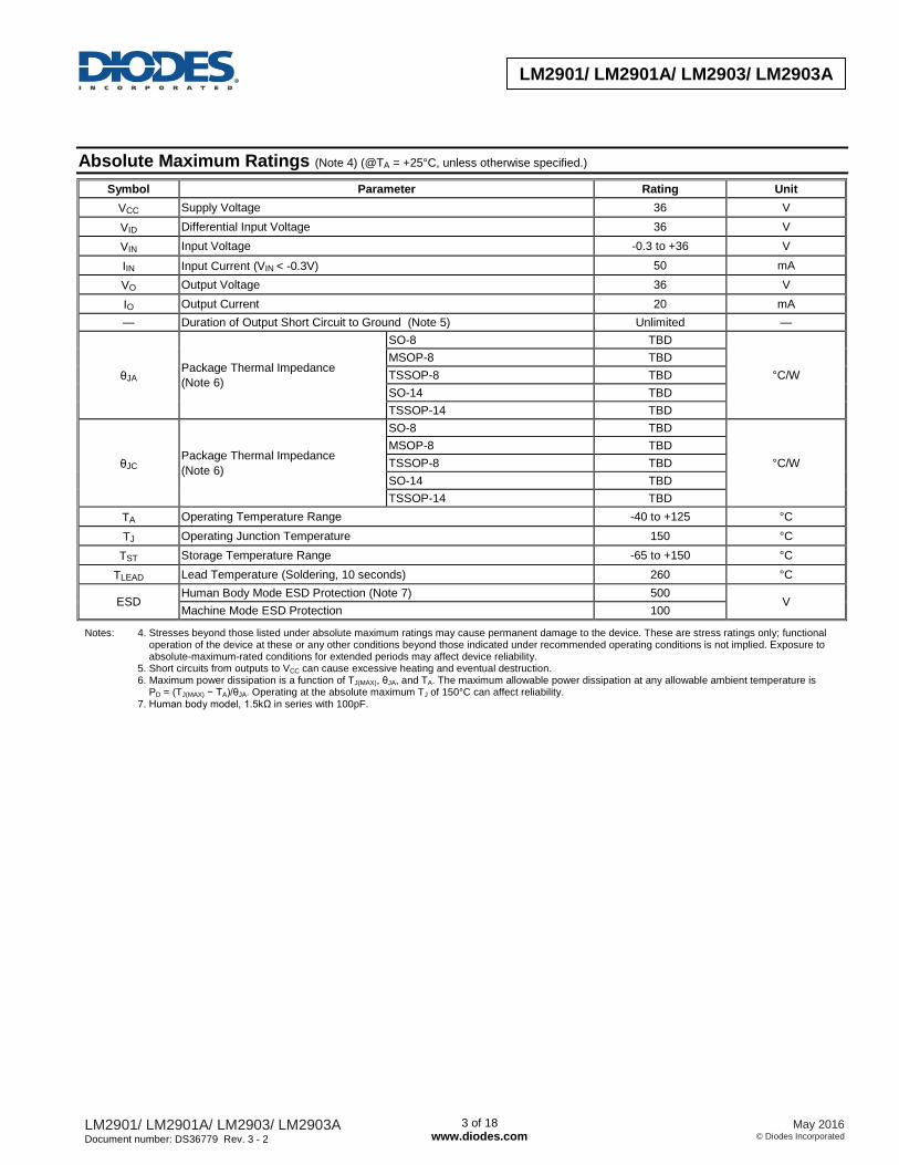
— Duration of Output Short Circuit to Ground (Note 5) Unlimited —
θJA Package Thermal Impedance
(Note 6)
SO-8 TBD
°C/W
MSOP-8 TBD
TSSOP-8 TBD
SO-14 TBD
TSSOP-14 TBD
θJC Package Thermal Impedance
(Note 6)
SO-8 TBD
°C/W
MSOP-8 TBD
TSSOP-8 TBD
SO-14 TBD
TSSOP-14 TBD
TA Operating Temperature Range -40 to +125 °C
TJ Operating Junction Temperature 150 °C
TST Storage Temperature Range -65 to +150 °C
TLEAD Lead Temperature (Soldering, 10 seconds) 260 °C
ESD Human Body Mode ESD Protection (Note 7) 500
V Machine Mode ESD Protection 100
Notes: 4. Stresses beyond those listed under absolute maximum ratings may cause permanent damage to the device. These are stress ratings only; functional operation of the device at these or any other conditions beyond those indicated under recommended operating conditions is not implied. Exposure to absolute-maximum-rated conditions for extended periods may affect device reliability. 5. Short circuits from outputs to VCC can cause excessive heating and eventual destruction. 6. Maximum power dissipation is a function of TJ(MAX), θJA, and TA. The maximum allowable power dissipation at any allowable ambient temperature is PD = (TJ(MAX) − TA)/θJA. Operating at the absolute maximum TJ of 150°C can affect reliability. 7. Human body model, 1.5kΩ in series with 100pF.
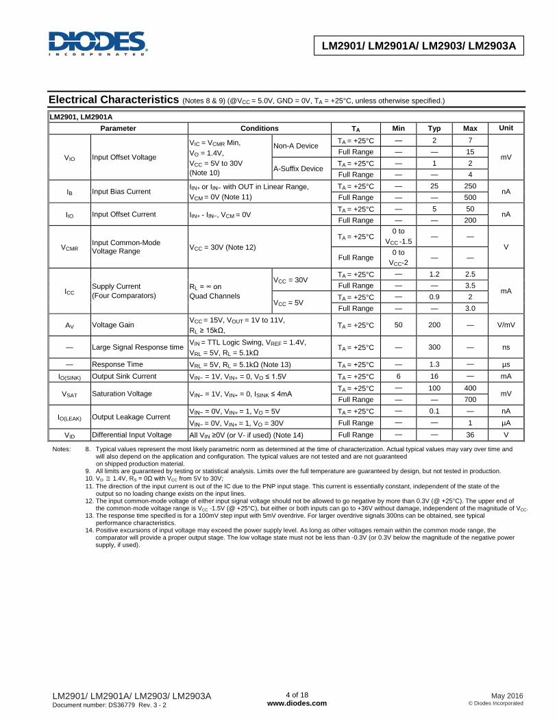
IB Input Bias Current IIN+ or IIN− with OUT in Linear Range,
VCM = 0V (Note 11)
TA = +25°C — 25 250 nA
Full Range — — 500
IIO Input Offset Current IIN+ - IIN−, VCM = 0V TA = +25°C — 5 50
nA Full Range — — 200
VCMR Input Common-Mode Voltage Range
VCC = 30V (Note 12)
TA = +25°C 0 to
VCC -1.5
— —
V
Full Range 0 to
VCC-2 — —
ICC Supply Current
(Four Comparators)
RL = ∞ on
Quad Channels
VCC = 30V TA = +25°C — 1.2 2.5
mA Full Range — — 3.5
VCC = 5V TA = +25°C — 0.9 2
Full Range — — 3.0
AV Voltage Gain VCC
= 15V, VOUT = 1V to 11V,
RL ≥ 15kΩ, TA = +25°C 50 200 — V/mV
— Large Signal Response time VIN
= TTL Logic Swing, VREF = 1.4V,
VRL = 5V, RL = 5.1kΩ TA = +25°C — 300 — ns
— Response Time VRL = 5V, RL = 5.1kΩ (Note 13) TA = +25°C — 1.3 — µs
IO(SINK) Output Sink Current VIN− = 1V, VIN+ = 0, VO ≤ 1.5V TA = +25°C 6 16 — mA
VSAT Saturation Voltage VIN− = 1V, VIN+ = 0, ISINK ≤ 4mA TA = +25°C — 100 400
mV Full Range — — 700
IO(LEAK) Output Leakage Current VIN− = 0V, VIN+ = 1, VO = 5V TA = +25°C — 0.1 — nA
VIN− = 0V, VIN+ = 1, VO = 30V Full Range — — 1 µA
VID Differential Input Voltage All VIN ≥0V (or V- if used) (Note 14) Full Range — — 36 V
Notes: 8. Typical values represent the most likely parametric norm as determined at the time of characterization. Actual typical values may vary over time and will also depend on the application and configuration. The typical values are not tested and are not guaranteed on shipped production material. 9. All limits are guaranteed by testing or statistical analysis. Limits over the full temperature are guaranteed by design, but not tested in production.
10. VO 1.4V, RS = 0Ω with VCC from 5V to 30V;
11. The direction of the input current is out of the IC due to the PNP input stage. This current is essentially constant, independent of the state of the output so no loading change exists on the input lines. 12. The input common-mode voltage of either input signal voltage should not be allowed to go negative by more than 0.3V (@ +25°C). The upper end of the common-mode voltage range is VCC -1.5V (@ +25°C), but either or both inputs can go to +36V without damage, independent of the magnitude of VCC. 13. The response time specified is for a 100mV step input with 5mV overdrive. For larger overdrive signals 300ns can be obtained, see typical performance characteristics. 14. Positive excursions of input voltage may exceed the power supply level. As long as other voltages remain within the common mode range, the
comparator will provide a proper output stage. The low voltage state must not be less than -0.3V (or 0.3V below the magnitude of the negative power supply, if used).
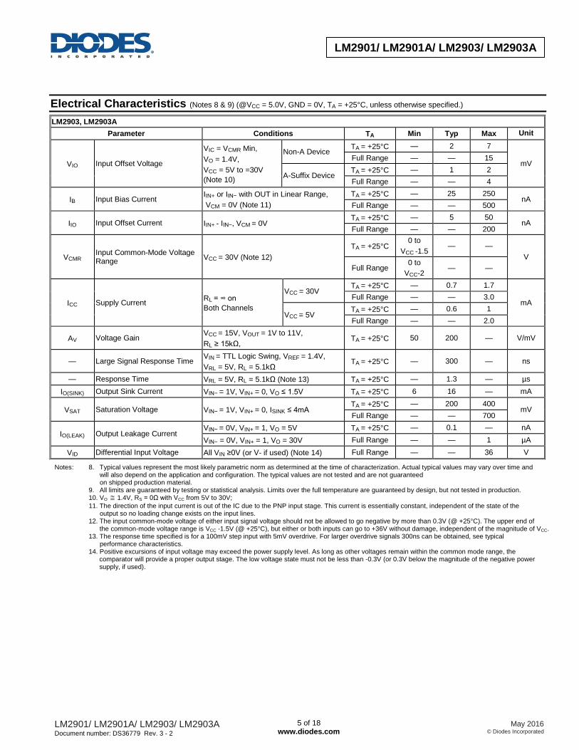
IB Input Bias Current IIN+ or IIN− with OUT in Linear Range,
VCM = 0V (Note 11)
TA = +25°C — 25 250 nA
Full Range — — 500
IIO Input Offset Current IIN+ - IIN−, VCM = 0V TA = +25°C — 5 50
nA Full Range — — 200
VCMR Input Common-Mode Voltage Range
VCC = 30V (Note 12)
TA = +25°C 0 to
VCC -1.5
— —
V
Full Range 0 to
VCC-2 — —
ICC Supply Current RL = ∞ on
Both Channels
VCC = 30V TA = +25°C — 0.7 1.7
mA Full Range — — 3.0
VCC = 5V
TA = +25°C — 0.6 1
Full Range — — 2.0
AV Voltage Gain VCC
= 15V, VOUT = 1V to 11V,
RL ≥ 15kΩ, TA = +25°C 50 200 — V/mV
— Large Signal Response Time VIN = TTL Logic Swing, VREF = 1.4V,
VRL = 5V, RL = 5.1kΩ TA = +25°C — 300 — ns
— Response Time VRL = 5V, RL = 5.1kΩ (Note 13) TA = +25°C — 1.3 — µs
IO(SINK) Output Sink Current VIN− = 1V, VIN+ = 0, VO ≤ 1.5V TA = +25°C 6 16 — mA
VSAT Saturation Voltage VIN− = 1V, VIN+ = 0, ISINK ≤ 4mA TA = +25°C — 200 400
mV Full Range — — 700
IO(LEAK) Output Leakage Current VIN− = 0V, VIN+ = 1, VO = 5V TA = +25°C — 0.1 — nA
VIN− = 0V, VIN+ = 1, VO = 30V Full Range — — 1 µA
VID Differential Input Voltage All VIN ≥0V (or V- if used) (Note 14) Full Range — — 36 V
Notes: 8. Typical values represent the most likely parametric norm as determined at the time of characterization. Actual typical values may vary over time and will also depend on the application and configuration. The typical values are not tested and are not guaranteed on shipped production material. 9. All limits are guaranteed by testing or statistical analysis. Limits over the full temperature are guaranteed by design, but not tested in production.
10. VO 1.4V, RS = 0Ω with VCC from 5V to 30V;
11. The direction of the input current is out of the IC due to the PNP input stage. This current is essentially constant, independent of the state of the output so no loading change exists on the input lines. 12. The input common-mode voltage of either input signal voltage should not be allowed to go negative by more than 0.3V (@ +25°C). The upper end of the common-mode voltage range is VCC -1.5V (@ +25°C), but either or both inputs can go to +36V without damage, independent of the magnitude of VCC. 13. The response time specified is for a 100mV step input with 5mV overdrive. For larger overdrive signals 300ns can be obtained, see typical performance characteristics. 14. Positive excursions of input voltage may exceed the power supply level. As long as other voltages remain within the common mode range, the
comparator will provide a proper output stage. The low voltage state must not be less than -0.3V (or 0.3V below the magnitude of the negative power supply, if used).
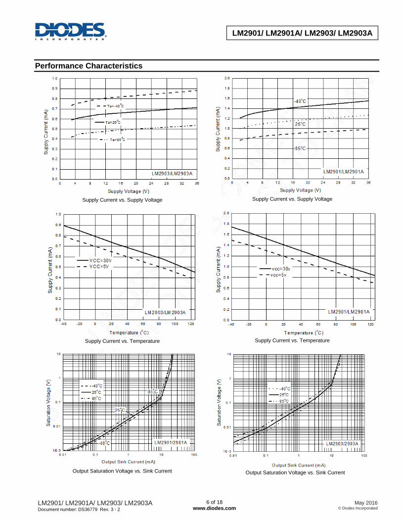
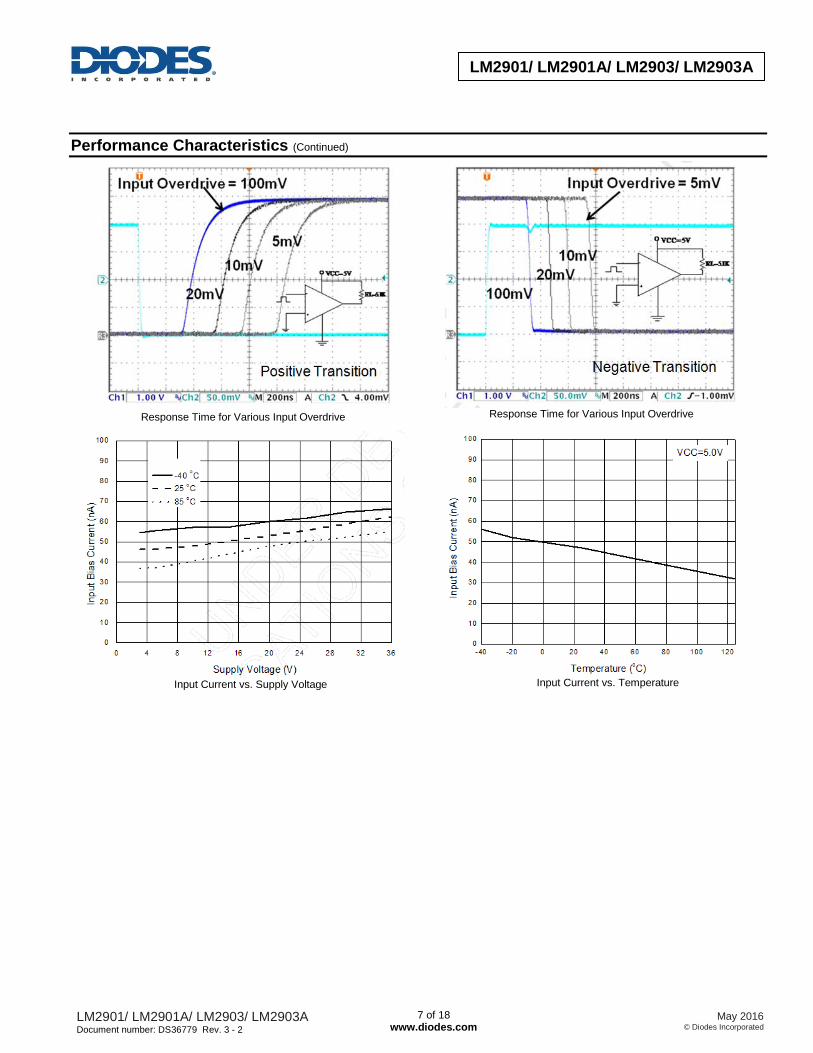
The LM2901/2903 series comparators are high-gain, wide bandwidth devices. Like most comparators, the series can easily oscillate if the output
lead is inadvertently allowed to capacitive couple to the inputs via stray capacitance. This shows up only during the output voltage transition
intervals as the comparators change states. Standard PC board layout is helpful as it reduces stray input-output coupling. Reducing the input
resistors to <10kΩ reduces the feedback signal levels. Finally, adding even a small amount (1.0 to 10 mV) of positive feedback (hysteresis) causes
such a rapid transition that oscillations, due to stray feedback, are not possible. Simply socketing the IC and attaching resistors to the pins will
cause input-output oscillations during the small transition intervals unless hysteresis is used. If the input signal is a pulse waveform, with relatively
fast rise and fall times, hysteresis is not required. All input pins of any unused comparators should be tied to the negative supply.
The bias network of the LM2901/2903 series comparators establishes a quiescent current independent of the magnitude of the power supply
voltage over the range of from 2.0VDC to 30VDC.
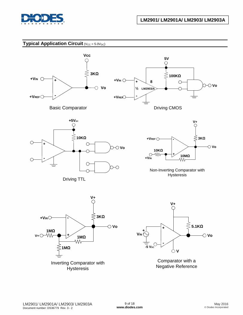
The differential input voltage may be larger than VCC without damaging the device. Protection should be provided to prevent the input voltages from
going negative more than -0.3VDC (@ +25°C). An input clamp diode can be used as shown in the applications section.
The output of the LM2901/2903 series comparators is the uncommitted collector of a grounded-emitter NPN output transistor. Many collectors can
be tied together to provide an output OR’ing function. An output pull-up resistor can be connected to any available power supply voltage within the
permitted supply voltage range and there is no restriction on this voltage due to the magnitude of the voltage applied to the VCC terminal of
LM2901/2903 series comparator package. The output can also be used as a simple SPST switch to ground (when a pull-up resistor is not used).
The amount of current the output device can sink is limited by the drive available (which is independent of VCC) and the β of this device. When the
maximum current limit is reached (approximately 16mA), the output transistor will come out of saturation and the output voltage will rise very
rapidly. The output saturation voltage is limited by the approximately 60Ω RSAT of the output transistor. The low offset voltage of the output
transistor (1.0mV) allows the output to clamp essentially to ground level for small load currents.
IMPORTANT NOTICE DIODES INCORPORATED MAKES NO WARRANTY OF ANY KIND, EXPRESS OR IMPLIED, WITH REGARDS TO THIS DOCUMENT, INCLUDING, BUT NOT LIMITED TO, THE IMPLIED WARRANTIES OF MERCHANTABILITY AND FITNESS FOR A PARTICULAR PURPOSE (AND THEIR EQUIVALENTS UNDER THE LAWS OF ANY JURISDICTION). Diodes Incorporated and its subsidiaries reserve the right to make modifications, enhancements, improvements, corrections or other changes without further notice to this document and any product described herein. Diodes Incorporated does not assume any liability arising out of the application or use of this document or any product described herein; neither does Diodes Incorporated convey any license under its patent or trademark rights, nor the rights of others. Any Customer or user of this document or products described herein in such applications shall assume all risks of such use and will agree to hold Diodes Incorporated and all the companies whose products are represented on Diodes Incorporated website, harmless against all damages. Diodes Incorporated does not warrant or accept any liability whatsoever in respect of any products purchased through unauthorized sales channel. Should Customers purchase or use Diodes Incorporated products for any unintended or unauthorized application, Customers shall indemnify and hold Diodes Incorporated and its representatives harmless against all claims, damages, expenses, and attorney fees arising out of, directly or indirectly, any claim of personal injury or death associated with such unintended or unauthorized application. Products described herein may be covered by one or more United States, international or foreign patents pending. Product names and markings noted herein may also be covered by one or more United States, international or foreign trademarks. This document is written in English but may be translated into multiple languages for reference. Only the English version of this document is the final and determinative format released by Diodes Incorporated.
LIFE SUPPORT Diodes Incorporated products are specifically not authorized for use as critical components in life support devices or systems without the express written approval of the Chief Executive Officer of Diodes Incorporated. As used herein: A. Life support devices or systems are devices or systems which: 1. are intended to implant into the body, or
2. support or sustain life and whose failure to perform when properly used in accordance with instructions for use provided in the labeling can be reasonably expected to result in significant injury to the user.