1 / 12 TriGem Micro-ATX Motherboard (Napoli-2) Table of Contents I. Introduction 1. Generation Description ------------------------------------------------------------ 2 2. Function Block Diagram ------------------------------------------------------------ 3 II. System Overview 1. Major Units ------------------------------------------------------------------------- 4 2. Upgradeability -------------------------------------------------------------------- 5 2-1. Processor -------------------------------------------------------------------- 5 2-2. Memory --------------------------------------------------------------------- 5 2-3. BIOS ------------------------------------------------------------------------- 6 2-4. Expansion Slot ------------------------------------------------------------ 6 2-5. Advanced Configuration and Power Interface (ACPI)----------------- 7 2-5. Manufacturing Options ------------------------------------------------------- 7 III. Jumper & Connector Description 1. Motherboard Jumper Setting------------------------------------------------------- 8 1-1. DIP Switch Setting Method ----------------------------------------------- 8 2. Motherboard Connector Description ------------------------------------------- 9 2-1. Motherboard Internal Connector --------------------------------------- 9 2-2. Motherboard External I/O Port ------------------------------------------- 12 3. Joystick & USB daughter board ------------------------------------------------ 12
Transcript
1 / 12
TriGem Micro-ATX Motherboard (Napoli-2)
Table of Contents
I. Introduction
1. Generation Description ------------------------------------------------------------ 22. Function Block Diagram ------------------------------------------------------------ 3
II. System Overview
1. Major Units ------------------------------------------------------------------------- 42. Upgradeability -------------------------------------------------------------------- 5
3. Joystick & USB daughter board ------------------------------------------------ 12
2 / 12
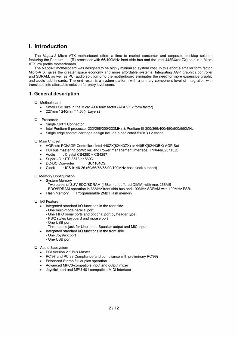
I. IntroductionThe Napoli-2 Micro ATX motherboard offers a time to market consumer and corporate desktop solution
featuring the Pentium-II,III(R) processor with 66/100MHz front side bus and the Intel 443BX(or ZX) sets in a MicroATX low profile motherboards
The Napoli-2 motherboard was designed to be highly minimized system cost. In this effort a smaller form factor,Micro-ATX, gives the greater space economy and more affordable systems. Integrating AGP graphics controllerand SDRAM, as well as PCI audio solution onto the motherboard eliminates the need for more expensive graphicand audio add-in cards. The end result is a system platform with a primary component level of integration withtranslates into affordable solution for entry level users.
1. General descriptionMotherboard• Small PCB size in the Micro ATX form factor (ATX V1.2 form factor)• 227mm * 240mm * 1.6t (4 Layers)
Processor• Single Slot 1 Connector• Intel Pentium-II processor 233/266/300/333MHz & Pentium-III 300/366/400/450/500/550MHz• Single edge contact cartridge design include a dedicated 512KB L2 cache
Main Chipset• AGPsets PCI/AGP Controller : Intel 440ZX(82443ZX) or 440BX(82443BX) AGP Set• PCI bus mastering controller, and Power management interface : PIIX4e(82371EB)• Audio : Crystal CS4280 + CS4297• Super I/O : ITE 8673 or 8693• DC-DC Converter : SC1164CS• Clock : ICS 9148-26 (60/66/75/83/90/100MHz host clock support)
Memory Configuration• System Memory
- Two banks of 3.3V EDO/SDRAM (168pin unbuffered DIMM) with max 256MB- EDO/SDRAM operation in 66MHz front side bus and 100MHz SDRAM with 100MHz FSB.
• Flash Memory : Programmable 2MB Flash memory
I/O Feature• Integrated standard I/O functions in the rear side
- One multi-mode parallel port- One FIFO serial ports and optional port by header type- PS/2 styles keyboard and mouse port- One USB port- Three audio jack for Line input, Speaker output and MIC input
• Integrated standard I/O functions in the front side- One Joystick port- One USB port
Audio Subsystem• PCI Version 2.1 Bus Master• PC’97 and PC’98 Compliance(and compliance with preliminary PC’99)• Enhanced Stereo full duplex operation• Advanced MPC3-compatible input and output mixer• Joystick port and MPU-401 compatible MIDI interface
3 / 12
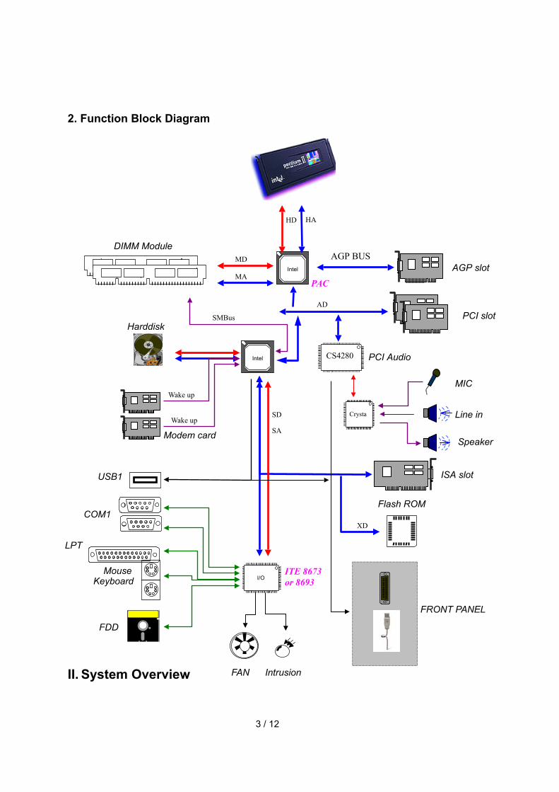
2. Function Block Diagram
II. System Overview
Intel
I/O
HD
MD
MA
XD
HA
AD
SMBus
Wake up
Wake upSD
SA
DIMM Module
PCI slotHarddisk
Intrusion
Modem card
FAN
USB1
COM1
LPT
Keyboard
ISA slot
Mouse
Flash ROM
FDD
AGP BUS
PAC
ITE 8673or 8693
CS4280 PCI Audio
AGP slot
Intel
Crysta
FRONT PANEL
MIC
Line in
Speaker
4 / 12
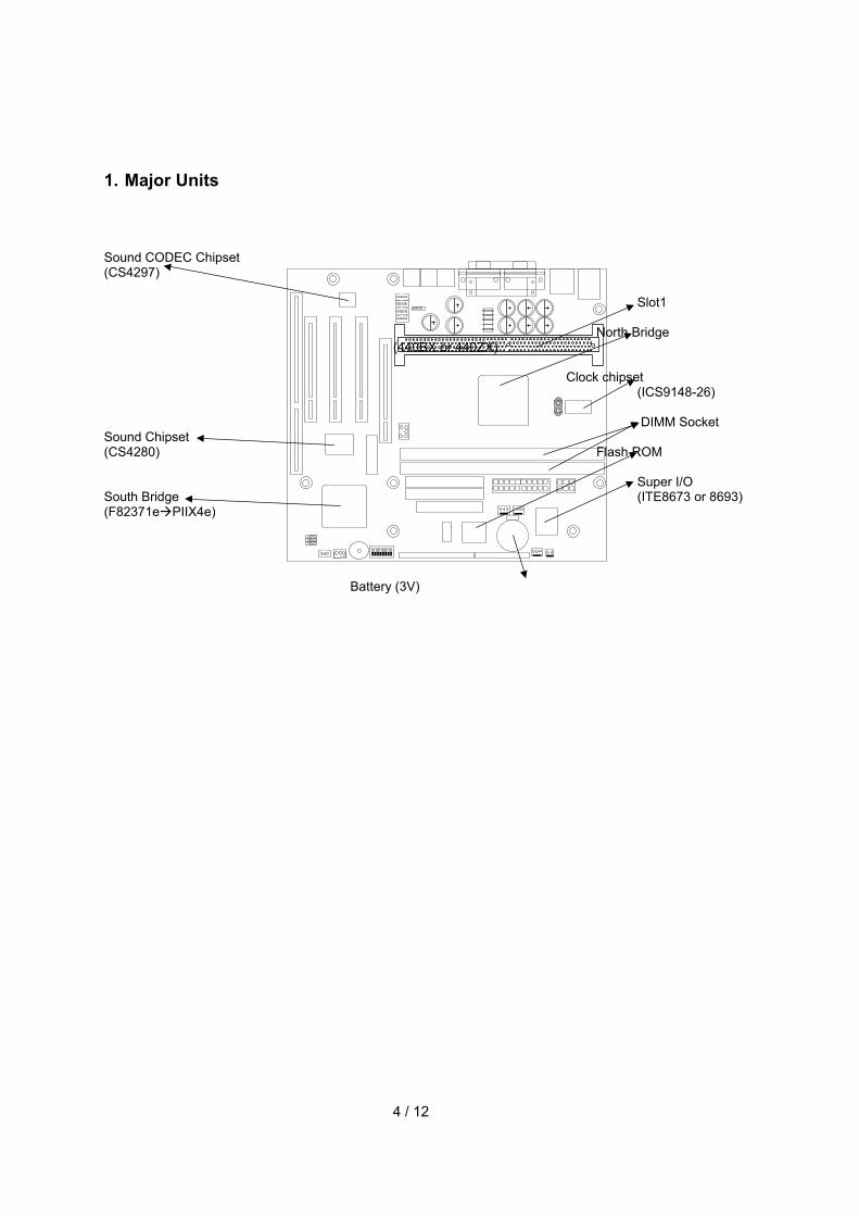
1. Major Units
Sound CODEC Chipset(CS4297)
Slot1
North Bridge (440BX or 440ZX)
Clock chipset(ICS9148-26)
DIMM SocketSound Chipset(CS4280) Flash ROM
Super I/OSouth Bridge (ITE8673 or 8693)(F82371e PIIX4e)
Battery (3V)
5 / 12
2. Upgradeability
This section describes the major specification of user upgrade parts. CPU, Memory, and extension slot will providea user to upgrade the overall performance by adding or changing these parts with other higher.
CPU : Pentium II processor 233/266/300/333/366MHz and Pentium III processor 350/400/450/500/550MHz Memory : EDO, SDRAM Modules (2bank, 16MB-256MB) Expansion slot : Three master PCI and One ISA slot One shared, One AGP slot
2-1. Processor
This motherboard supports a single Pentium II processor or Pentium III processor. The processor’s VID pinsautomatically program the voltage regulator, which is on the motherboard for the required processor voltage. Themotherboard supports processors that run internally at 300/333/300/350/400/450/500/550MHz, and have a512Kb second level cache.
Packing Expansion slot : Three master PCI and One ISA slot One shared, One AGP slot
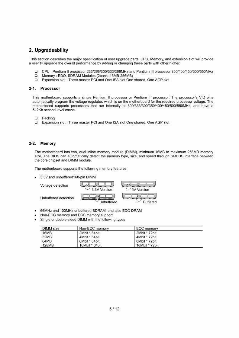
2-2. Memory
The motherboard has two, dual inline memory module (DIMM), minimum 16MB to maximum 256MB memorysize. The BIOS can automatically detect the memory type, size, and speed through SMBUS interface betweenthe core chipset and DIMM module.
The motherboard supports the following memory features
• 3.3V and unbuffered168-pin DIMM
Voltage detection3.3V Version 5V Version
Unbuffered detection Unbuffered Buffered
• 66MHz and 100MHz unbuffered SDRAM, and also EDO DRAM• Non-ECC memory and ECC memory support• Single or double-sided DIMM with the following types
The motherboard uses a TriGem-AMI BIOS, which is stored in flash memory and can be upgraded using a disk-based program. A new version of the BIOS can be upgraded from a diskette using the Flash Memory Updateutility.
Flash memory organization
Address (Hex) Size Functional descriptionFFFF0000 – FFFFFFFF 64KB Boot blockFFFA0000 – FFFEFFFF 256KB Main BIOS blockFF9F0000 - FFF9FFFF 8KB Used by BIOS (Event logging)FFF9E000 - FFF9EFFF 8KB OEM logo or can flash areaFFF9C000 - FFF9DFFF 16KB DMI configuration data, PnP,FFF90000 - FFF9BFFF 96KB Fault tolerant storageFFF80000 - FFF8FFFF 64KB Fault tolerant backup block
On-board device management
The BIOS can manage the devices on the motherboard over the CMOS setup menu. However the built-in AGPgraphics controller can be disabled by the corresponding jumper as described Jumper Setting section later.
Device Description CMOS setup menu Default valueInternal Cache Pentium Processor Enable / Disable EnabledPS/2 Mouse Super I/O (ITE8673 or 8693) Enable / Disable EnabledUSB Function South Bridge (PIIX4e) Enable / Disable EnabledOn board Sound CS4280 + CS4297 Enable / Disable EnabledOn board FDC Super I/O (ITE8673 or 8693) Auto / Enable / Disable AutoOn board serial Super I/O (ITE8673 or 8693) Auto / 3F8 / 2F8 / 3E8 / 2E8 AutoOn board parallel Super I/O (ITE8673 or 8693) Auto / Disable / 378 / 278 / 3BC AutoOn board IDE South Bridge (PIIX4e) Disable / Primary / Secondary / Both Both
2-4. Expansion Slot
The motherboard support ISA, PCI and AGP function. ISA and PCI functions are extended to the additional slotwith two ISA and two PCI, and AGP function is designed in the motherboard with AGP graphics controller.
PCI configuration space map
Bus number Device number Function number Device00 00 00 F82443BX or ZX (North bridge)00 01 00 PIIX4e (South bridge)00 07 00 PCI/ISA bridge (South bridge)00 07 01 IDE bus master (South bridge)00 07 02 USB (South bridge)00 07 03 Power management (South bridge)01 00 00 AGP Slot00 13 00 PCI slot100 12 00 PCI slot200 11 00 PCI slot302 10 00 CS4280(Sound Controller)
7 / 12
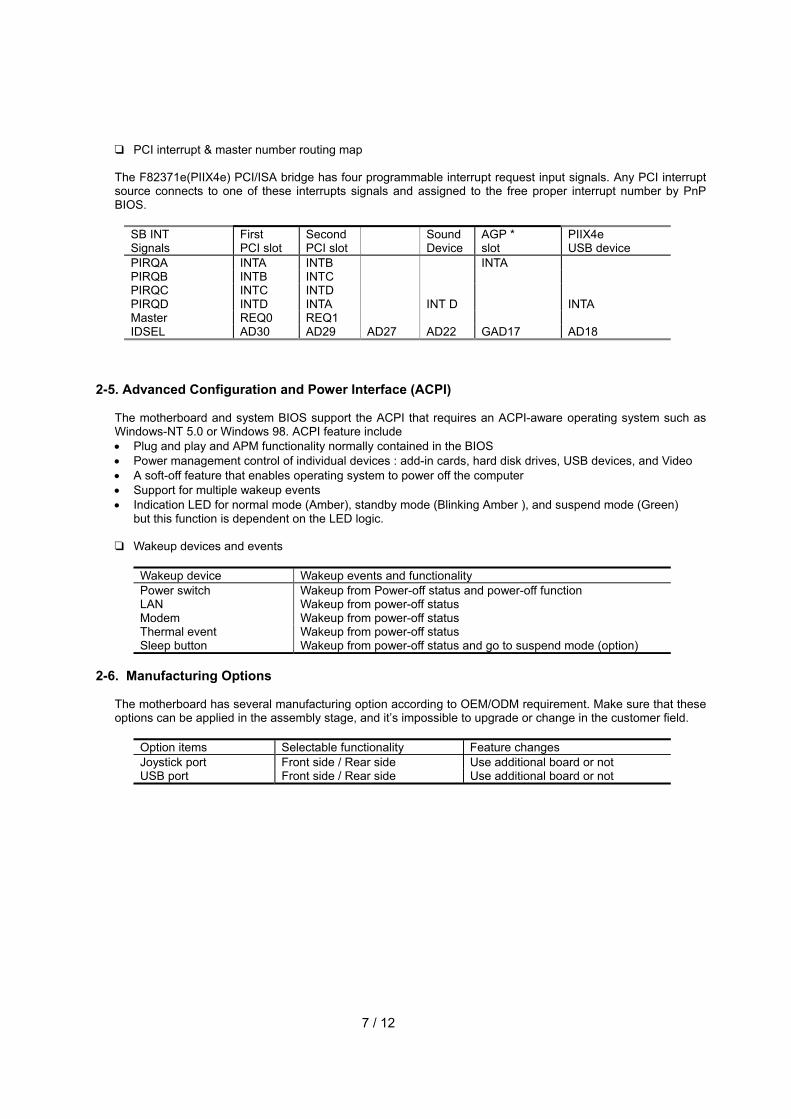
PCI interrupt & master number routing map
The F82371e(PIIX4e) PCI/ISA bridge has four programmable interrupt request input signals. Any PCI interruptsource connects to one of these interrupts signals and assigned to the free proper interrupt number by PnPBIOS.
2-5. Advanced Configuration and Power Interface (ACPI)
The motherboard and system BIOS support the ACPI that requires an ACPI-aware operating system such asWindows-NT 5.0 or Windows 98. ACPI feature include• Plug and play and APM functionality normally contained in the BIOS• Power management control of individual devices : add-in cards, hard disk drives, USB devices, and Video• A soft-off feature that enables operating system to power off the computer• Support for multiple wakeup events• Indication LED for normal mode (Amber), standby mode (Blinking Amber ), and suspend mode (Green)
but this function is dependent on the LED logic.
Wakeup devices and events
Wakeup device Wakeup events and functionalityPower switch Wakeup from Power-off status and power-off functionLAN Wakeup from power-off statusModem Wakeup from power-off statusThermal event Wakeup from power-off statusSleep button Wakeup from power-off status and go to suspend mode (option)
2-6. Manufacturing Options
The motherboard has several manufacturing option according to OEM/ODM requirement. Make sure that theseoptions can be applied in the assembly stage, and it’s impossible to upgrade or change in the customer field.
Option items Selectable functionality Feature changesJoystick port Front side / Rear side Use additional board or notUSB port Front side / Rear side Use additional board or not
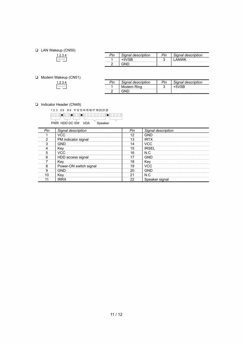
III. Jumper & Connector Description1. Motherboard Jumper Setting
1-1. DIP Switch Setting Method
CPU Freq Ratio
Ratio SW1 SW2 SW3 SW42x ON ON ON ON3x ON OFF ON ON4x OFF ON ON ON5x OFF OFF ON ON
2.5x ON ON OFF ON3.5x ON OFF OFF ON4.5x OFF ON OFF ON2x OFF OFF OFF OFF
Other functionality
DIP Switch Function ON OFFSW5 CMOS RAM function Clear CMOS RAM Enable write/saveSW6 Password function Clear password Enable passwordSW7 CMOS setup function Disable to edit CMOS contents Enable to edit CMOS contentsSW8 FDD write protect Disable to write data
to Floppy diskEnable to write data
to Floppy disk
1-2. Jumper Setting MethodOEM/ODM selector
These jumpers (J2,3, 7) will be optional parts for the OEM/ODM logo message selector.
For the proper operation, these jumpers should be set together.J2 J3 J7 ODM Vendor2-3 2-3 2-3 ODM2-3 2-3 1-2 Trigem Export2-3 1-2 2-3 Trigem Domestic2-3 1-2 1-2 Reserved