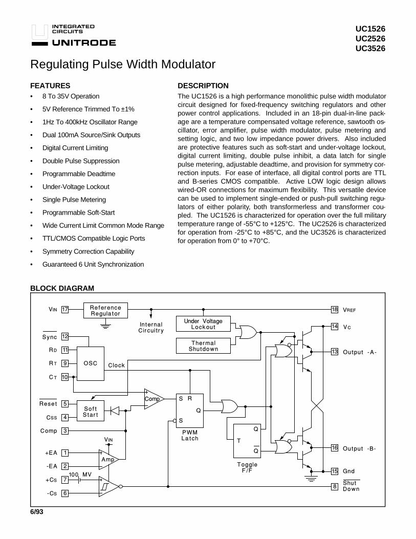
UC1526 UC2526 UC3526 DESCRIPTION The UC1526 is a high performance monolithic pulse width modulator circuit designed for fixed-frequency switching regulators and other power control applications. Included in an 18-pin dual-in-line pack- age are a temperature compensated voltage reference, sawtooth os- cillator, error amplifier, pulse width modulator, pulse metering and setting logic, and two low impedance power drivers. Also included are protective features such as soft-start and under-voltage lockout, digital current limiting, double pulse inhibit, a data latch for single pulse metering, adjustable deadtime, and provision for symmetry cor- rection inputs. For ease of interface, all digital control ports are TTL and B-series CMOS compatible. Active LOW logic design allows wired-OR connections for maximum flexibility. This versatile device can be used to implement single-ended or push-pull switching regu- lators of either polarity, both transformerless and transformer cou- pled. The UC1526 is characterized for operation over the full military temperature range of -55°C to +125°C. The UC2526 is characterized for operation from -25°C to +85°C, and the UC3526 is characterized for operation from 0° to +70°C. Regulating Pulse Width Modulator FEATURES • 8 To 35V Operation • 5V Reference Trimmed To ±1% • 1Hz To 400kHz Oscillator Range • Dual 100mA Source/Sink Outputs • Digital Current Limiting • Double Pulse Suppression • Programmable Deadtime • Under-Voltage Lockout • Single Pulse Metering • Programmable Soft-Start • Wide Current Limit Common Mode Range • TTL/CMOS Compatible Logic Ports • Symmetry Correction Capability • Guaranteed 6 Unit Synchronization BLOCK DIAGRAM 6/93
Transcript
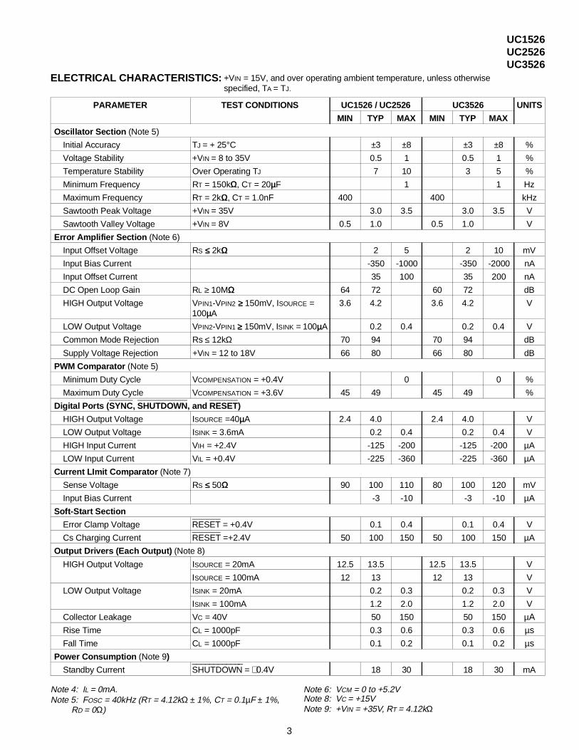
UC1526UC2526UC3526
DESCRIPTIONThe UC1526 is a high performance monolithic pulse width modulatorcircuit designed for fixed-frequency switching regulators and otherpower control applications. Included in an 18-pin dual-in-line pack-age are a temperature compensated voltage reference, sawtooth os-cillator, error amplifier, pulse width modulator, pulse metering andsetting logic, and two low impedance power drivers. Also includedare protective features such as soft-start and under-voltage lockout,digital current limiting, double pulse inhibit, a data latch for singlepulse metering, adjustable deadtime, and provision for symmetry cor-rection inputs. For ease of interface, all digital control ports are TTLand B-series CMOS compatible. Active LOW logic design allowswired-OR connections for maximum flexibility. This versatile devicecan be used to implement single-ended or push-pull switching regu-lators of either polarity, both transformerless and transformer cou-pled. The UC1526 is characterized for operation over the full militarytemperature range of -55°C to +125°C. The UC2526 is characterizedfor operation from -25°C to +85°C, and the UC3526 is characterizedfor operation from 0° to +70°C.
The reference regulator of the UC1526 is based on a tem-perature compensated zener diode. The circuitry is fullyactive at supply voltages above +8V, and provides up to20mA of load current to external circuitry at +5.0V. In sys-tems where additional current is required, an externalPNP transistor can be used to boost the available current.A rugged low frequency audio-type transistor should beused, and lead lengths between the PWM and transistorshould be as short as possible to minimize the risk of os-cillations. Even so, some types of transistors may requirecollector-base capacitance for stability. Up to 1 amp ofload current can be obtained with excellent regulation ifthe device selected maintains high current gain.
Under-Voltage Lockout
The under-voltage lockout circuit protects the UC1526and the power devices it controls from inadequate supplyvoltage, If +VIN is too low, the circuit disables the outputdrivers and holds the RESET
_______ pin LOW. This prevents
spurious output pulses while the control circuitry is stabi-lizing, and holds the soft-start timing capacitor in a dis-charged state.
The circuit consists of a +1.2V bandgap reference andcomparator circuit which is active when the referencevoltage has risen to 3VBE or +1.8V at 25°C. When the ref-erence voltage rises to approximately +4.4V, the circuitenables the output drivers and releases the RESET
_______ pin,
allowing a normal soft-start. The comparator has 200mVof hysteresis to minimize oscillation at the trip point.When +VIN to the PWM is removed and the referencedrops to +4.2V, the under-voltage circuit pulls RESET
_______
LOW again. The soft-start capacitor is immediately dis-charged, and the PWM is ready for another soft-start cy-cle.
The UC1526 can operate from a +5V supply by connect-ing the VREF pin to the +VIN pin and maintaining the sup-ply between +4.8 and +5.2V.
Soft-Start Circuit
The soft-start circuit protects the power transistors andrectifier diodes from high current surges during powersupply turn-on. When supply voltage is first applied to theUC1526, the under-voltage lockout circuit holds RESET
_______
LOW with Q3. Q1 is turned on, which holds the soft-startcapacitor voltage at zero. The second collector of Q1
clamps the output of the error amplifier to ground, guaran-teeing zero duty cycle at the driver outputs. When thesupply voltage reaches normal operating range, RESET
_______
will go HIGH. Q1 turns off, allowing the internal 100mAcurrent source to charge CS. Q2 clamps the error ampli-fier output to 1VBE above the voltage on CS. As the soft-start voltage ramps up to +5V, the duty cycle of the PWMlinearly increases to whatever value the voltage regula-tion loop requires for an error null.
Digital Control Ports
The three digital control ports of the UC1526 are bi-direc-tional. Each pin can drive TTL and 5V CMOS logic di-rectly, up to a fan-out of 10 low-power Schottky gates.Each pin can also be directly driven by open-collector
Figure 2. Under-Voltage Lockout Schematic
Figure 1. Extending Reference Output Current
Figure 3. Soft-Start Circuit Schematic
4
TTL, open-drain CMOS, and open-collector voltage com-parators; fan-in is equivalent to 1 low-power Schottkygate. Each port is normally HIGH; the pin is pulled LOWto activate the particular function. Driving SYNC
______ LOW in-
itiates a discharge cycle in the oscillator. PullingSHUTDOWN____________
LOW immediately inhibits all PWM outputpulses. Holding RESET
_______ LOW discharges the soft-start
capacitor. The logic threshold is +1.1V at +25°C. Noiseimmunity can be gained at the expense of fan-out with anexternal 2k pull-up resistor to +5V.
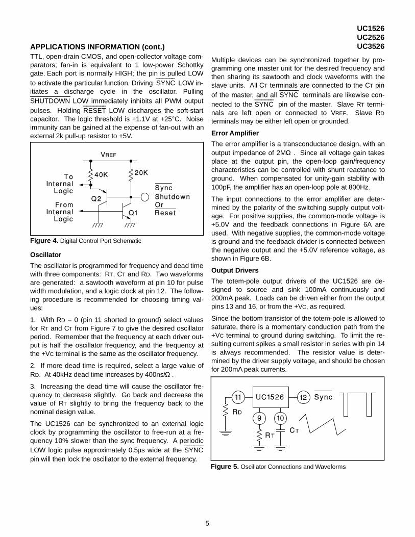
Oscillator
The oscillator is programmed for frequency and dead timewith three components: RT, CT and RD. Two waveformsare generated: a sawtooth waveform at pin 10 for pulsewidth modulation, and a logic clock at pin 12. The follow-ing procedure is recommended for choosing timing val-ues:
1. With RD = 0 (pin 11 shorted to ground) select valuesfor RT and CT from Figure 7 to give the desired oscillatorperiod. Remember that the frequency at each driver out-put is half the oscillator frequency, and the frequency atthe +VC terminal is the same as the oscillator frequency.
2. If more dead time is required, select a large value ofRD. At 40kHz dead time increases by 400ns/Ω .
3. Increasing the dead time will cause the oscillator fre-quency to decrease slightly. Go back and decrease thevalue of RT slightly to bring the frequency back to thenominal design value.
The UC1526 can be synchronized to an external logicclock by programming the oscillator to free-run at a fre-quency 10% slower than the sync frequency. A periodicLOW logic pulse approximately 0.5µs wide at the SYNC
______
pin will then lock the oscillator to the external frequency.
Multiple devices can be synchronized together by pro-gramming one master unit for the desired frequency andthen sharing its sawtooth and clock waveforms with theslave units. All CT terminals are connected to the CT pinof the master, and all SYNC
______ terminals are likewise con-
nected to the SYNC______
pin of the master. Slave RT termi-nals are left open or connected to VREF. Slave RD
terminals may be either left open or grounded.
Error Amplifier
The error amplifier is a transconductance design, with anoutput impedance of 2MΩ . Since all voltage gain takesplace at the output pin, the open-loop gain/frequencycharacteristics can be controlled with shunt reactance toground. When compensated for unity-gain stability with100pF, the amplifier has an open-loop pole at 800Hz.
The input connections to the error amplifier are deter-mined by the polarity of the switching supply output volt-age. For positive supplies, the common-mode voltage is+5.0V and the feedback connections in Figure 6A areused. With negative supplies, the common-mode voltageis ground and the feedback divider is connected betweenthe negative output and the +5.0V reference voltage, asshown in Figure 6B.
Output Drivers
The totem-pole output drivers of the UC1526 are de-signed to source and sink 100mA continuously and200mA peak. Loads can be driven either from the outputpins 13 and 16, or from the +VC, as required.
Since the bottom transistor of the totem-pole is allowed tosaturate, there is a momentary conduction path from the+VC terminal to ground during switching. To limit the re-sulting current spikes a small resistor in series with pin 14is always recommended. The resistor value is deter-mined by the driver supply voltage, and should be chosenfor 200mA peak currents.
UC1526UC2526UC3526
Figure 5. Oscillator Connections and Waveforms
Figure 4. Digital Control Port Schematic
APPLICATIONS INFORMATION (cont.)
5
UC1526UC2526UC3526
Figure 6. Error Amplifier Connections
Figure 7. Push-Pull Configuration
Figure 8. Single-Ended Configuration
Figure 9. Driving N-channel Power Mosfets
Oscillation Period
TYPICAL CHARACTERISTICSOscillator Period vs R T and CT
Output Driver Deadtime vs R D Value Under Voltage Lockout Characteristic
Error Amplifier Open Loop Gain vs Frequency Current Limit Transfer Function
7
IMPORTANT NOTICE
Texas Instruments and its subsidiaries (TI) reserve the right to make changes to their products or to discontinueany product or service without notice, and advise customers to obtain the latest version of relevant informationto verify, before placing orders, that information being relied on is current and complete. All products are soldsubject to the terms and conditions of sale supplied at the time of order acknowledgement, including thosepertaining to warranty, patent infringement, and limitation of liability.
TI warrants performance of its semiconductor products to the specifications applicable at the time of sale inaccordance with TI’s standard warranty. Testing and other quality control techniques are utilized to the extentTI deems necessary to support this warranty. Specific testing of all parameters of each device is not necessarilyperformed, except those mandated by government requirements.
CERTAIN APPLICATIONS USING SEMICONDUCTOR PRODUCTS MAY INVOLVE POTENTIAL RISKS OFDEATH, PERSONAL INJURY, OR SEVERE PROPERTY OR ENVIRONMENTAL DAMAGE (“CRITICALAPPLICATIONS”). TI SEMICONDUCTOR PRODUCTS ARE NOT DESIGNED, AUTHORIZED, ORWARRANTED TO BE SUITABLE FOR USE IN LIFE-SUPPORT DEVICES OR SYSTEMS OR OTHERCRITICAL APPLICATIONS. INCLUSION OF TI PRODUCTS IN SUCH APPLICATIONS IS UNDERSTOOD TOBE FULLY AT THE CUSTOMER’S RISK.
In order to minimize risks associated with the customer’s applications, adequate design and operatingsafeguards must be provided by the customer to minimize inherent or procedural hazards.
TI assumes no liability for applications assistance or customer product design. TI does not warrant or representthat any license, either express or implied, is granted under any patent right, copyright, mask work right, or otherintellectual property right of TI covering or relating to any combination, machine, or process in which suchsemiconductor products or services might be or are used. TI’s publication of information regarding any thirdparty’s products or services does not constitute TI’s approval, warranty or endorsement thereof.