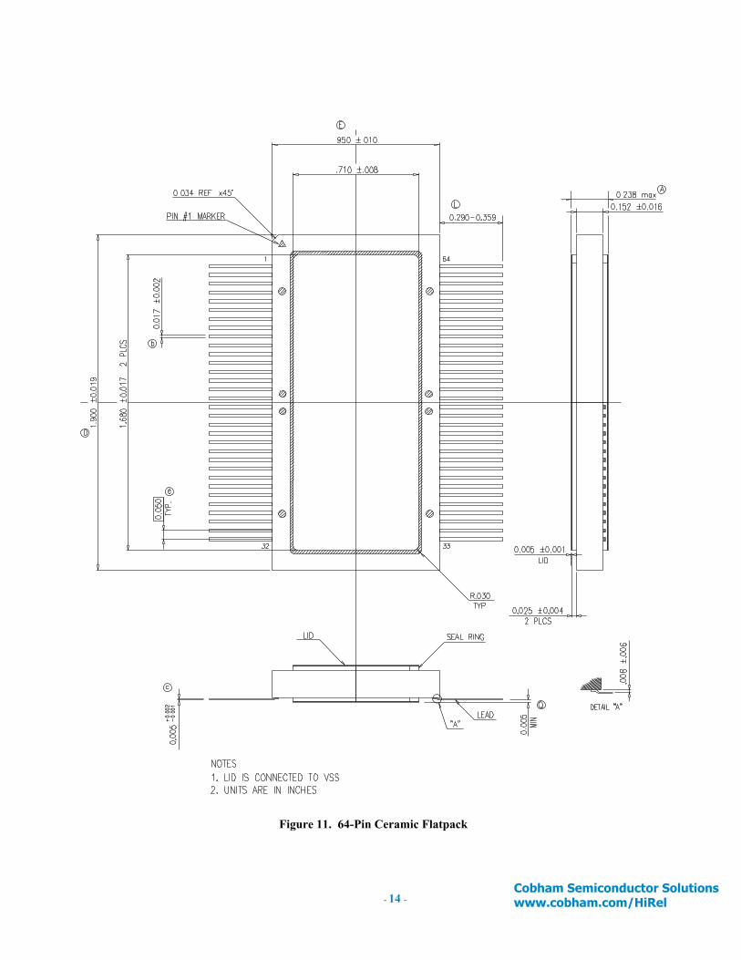
The most important thing we build is trust Cobham Semiconductor Solutions www.cobham.com/HiRel - 1 - FEATURES Single 3.3-V power supply Fast 50ns read/write access time Functionally compatible with traditional asynchronous SRAMs Equal address and chip-enable access times HiRel temperature range (-40 o C to +105 o C) Automatic data protection with low-voltage inhibit circuitry to prevent writes on power loss CMOS and TTL compatible Data non-volatile for > 20 years (-40 o C to +105 o C) Read/Write endurance: Unlimited for 20 years (-40 o C to +105 o C) 64-pin ceramic flatpack package (21.99 grams) Operational environment: - Total dose: 1 Mrad(Si) - SEL Immune: 112 MeV-cm 2 /mg @125 o C - SEU Immune: Memory Cell 112 MeV-cm 2 /mg @25 o C Standard Microelectronics Drawing (SMD) - 5962-13207 - QML Q, Q+, and V (V pending contact factory) INTRODUCTION The Cobham (formerly Aeroflex) 64Megabit Non-Volatile magnetoresistive random access memory (MRAM) is a high- performance memory multichip module (MCM) compatible with traditional asynchronous SRAM operations, organized as either four 2M words by 8 bits or one 8M words by 8 bits. The MRAM is equipped with five chip enables (/En), a single write enable (/W), and a single output enable (/G) pins, allowing for significant system design flexibility without bus contention. Data is non-volatile for > 20 years at temperature and data is automatically protected against power loss by a low voltage write inhibit. The 64Mb MRAM is designed specifically for operation in HiREL environments. As shown in Table 4, the magneto-resistive bit cells are immune to Single Event Effects (SEE). To guard against transient effects, an Error Correction Code (ECC) is included within the device. ECC check bits are generated and stored within the MRAM array during writes. The MBE pin identifies that ECC logic has detected two bit errors during the current read cycle. Figure 1. UT8MR8M8 MRAM Block Diagram Standard Products UT8MR8M8 64Megabit Non-Volatile MRAM Datasheet September, 2019
Transcript
The most important thing we build is trust
M
Standard ProductsUT8MR8M8 64Megabit Non-Volatile MRAM Datasheet September, 2019
FEATURES Single 3.3-V power supply Fast 50ns read/write access time Functionally compatible with traditional asynchronous SRAMs Equal address and chip-enable access times HiRel temperature range (-40oC to +105oC) Automatic data protection with low-voltage inhibit circuitry to
prevent writes on power loss CMOS and TTL compatible Data non-volatile for > 20 years (-40oC to +105oC) Read/Write endurance: Unlimited for 20 years (-40oC to +105oC) 64-pin ceramic flatpack package (21.99 grams) Operational environment:
- Total dose: 1 Mrad(Si)- SEL Immune: 112 MeV-cm2/mg @125oC- SEU Immune: Memory Cell 112 MeV-cm2/mg @25oC
Standard Microelectronics Drawing (SMD) - 5962-13207- QML Q, Q+, and V (V pending contact factory)
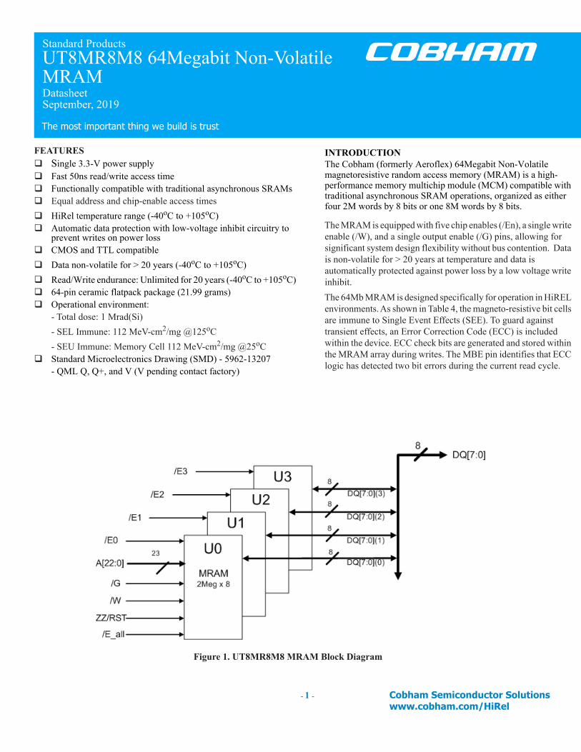
Figure 1. UT8MR8M8 MRA
- 1 -
INTRODUCTIONThe Cobham (formerly Aeroflex) 64Megabit Non-Volatile magnetoresistive random access memory (MRAM) is a high-performance memory multichip module (MCM) compatible with traditional asynchronous SRAM operations, organized as either four 2M words by 8 bits or one 8M words by 8 bits.
The MRAM is equipped with five chip enables (/En), a single write enable (/W), and a single output enable (/G) pins, allowing for significant system design flexibility without bus contention. Data is non-volatile for > 20 years at temperature and data is automatically protected against power loss by a low voltage write inhibit.The 64Mb MRAM is designed specifically for operation in HiREL environments. As shown in Table 4, the magneto-resistive bit cells are immune to Single Event Effects (SEE). To guard against transient effects, an Error Correction Code (ECC) is included within the device. ECC check bits are generated and stored within the MRAM array during writes. The MBE pin identifies that ECC logic has detected two bit errors during the current read cycle.
The UT8MR8M8 has control inputs called Chip Enable (E[3:0]), Chip Enable All (/E_ALL), Write Enable (/W), Output Enable (/G), and sleep/reset mode (ZZ/RST); 23 address inputs, A[22:0]; eight bidirectional data lines, DQ[7:0]; and a Multi-bit Error Flag (MBE). /E[3:0] controls device selection, active, and standby modes. Asserting /E[3:0] enables the device, causes IDD to rise to its active value, and decodes the 21 address inputs, A[20:0], to select one of 16,777,216 words in the memory. Note: Only one Chip Enable may be active at any time. Asserting /E_ALL allows the device to be addressed as a single, 64Mb memory using address bits A21 and A22 to decode and select 1 of 4 MRAM die. /W controls read and write operation. During a read cycle, /G must be asserted to enable the outputs. ZZ/RST controls the sleep/reset mode operation and provides device reset capability. Enabling sleep/reset mode causes all other inputs to be don't cares. ZZ/RST places all die into internal low power even while system power is still applied to VDD. The MBE pin is an open drain output pin which allows for wired-OR of multiple MBE when using multiple MRAMs. The MBE pin requires an external pull up to reach the high inactive state. See MRAM FAQ to determine the resistor value. When MBE is low, it identifies that a two bit error exists for the read cycle.
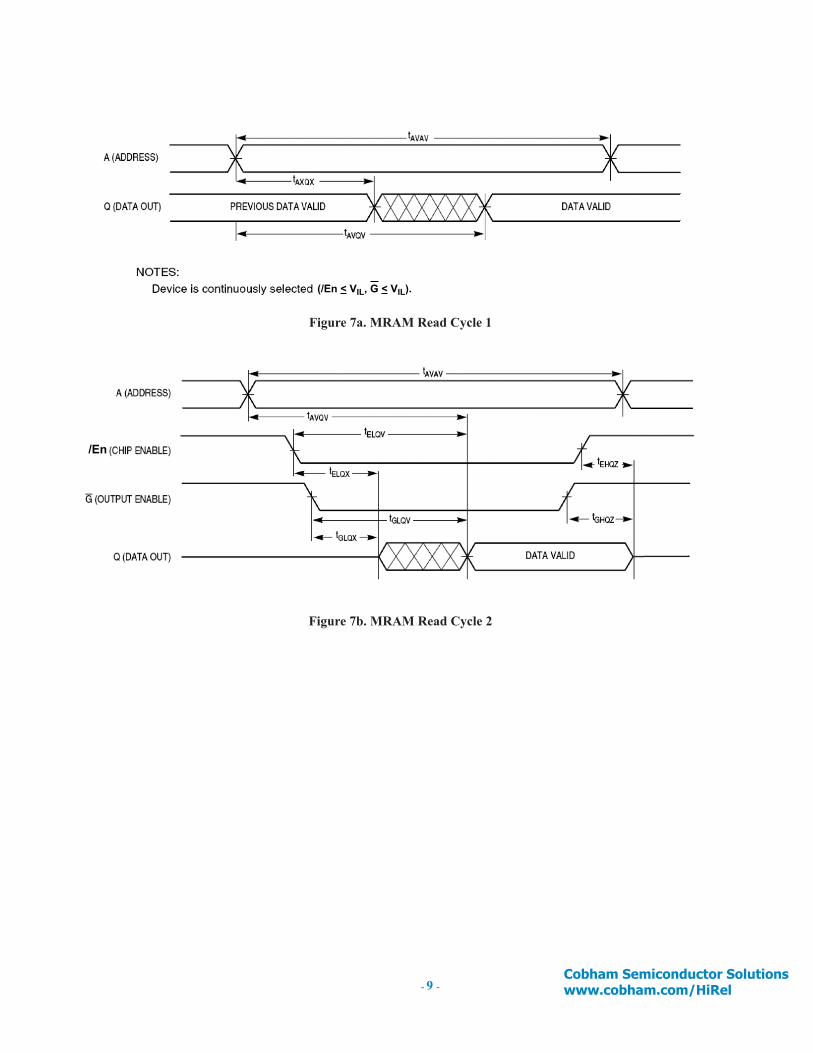
A combination of /W greater than VIH (min) and a single /En less than VIL (max) defines a read cycle. Read access time is measured from the latter of chip enable, output enable, or valid address to valid data output.
MRAM Read Cycle 1, the Address Access in Figure 4a, is initiated by a change in address inputs after a single /En is asserted, /G asserted and /W deasserted. Valid data appears on data outputs DQ[7:0] after the specified tAVQV is satisfied. Outputs remain active throughout the entire cycle. As long as a single chip enable and output enable are active, the address inputs may change at a rate equal to the minimum read cycle time (tAVAV).
MRAM Read Cycle 2, the Chip Enable-controlled Access in Figure 4b, is initiated by a single /En going active while /G remains asserted, /W remains deasserted, and the addresses remain stable for the entire cycle. After the specified tELQV is satisfied, the eight-bit word addressed by A[20:0] is accessed and appears at the data outputs DQ[7:0].
WRITE CYCLE
A combination of /W and a single /En less than VIL(max) defines a write cycle. The state of /G is a “don’t care” for a write cycle. The outputs are placed in the high-impedance state when either /G is greater than VIH(min), or when /W is less than VIL(max).
Write Cycle 1, the Write Enable-controlled Access in Figure 5a, is defined by a write terminated by /W going high, with a single /En still active. The write pulse width is defined by tWLWH when the write is initiated by /W, and by tETWH when the write is initiated by a single /En. Unless the outputs have been previously placed in the high-impedance state by /G, the user must wait tWLQZ before applying data to the nine bidirectional pins DQ[7:0] to avoid bus contention.
Write Cycle 2, the Chip Enable-controlled Access in Figure 5b, is defined by a write terminated by a single /En going inactive. The write pulse width is defined by tWLEH when the write is initiated by /W, and by tELEH when the write is initiated by a single /En going active. For the /W initiated write, unless the outputs have been previously placed in the high-impedance state by /G, the user must wait tWLQZ before applying data to the eight bidirectional pins DQ[7:0] to avoid bus contention.
OPERATIONAL ENVIRONMENT
The UT8MR8M8 MRAM incorporates special design and layout features which allows operation in harsh environments.
Notes:1. SEL test performed at VDD = 3.6V and temperature = 125oC.2. SEU test performed at VDD = 3.0V and unpowered at room temperature.
POWER UP AND POWER DOWN SEQUENCING
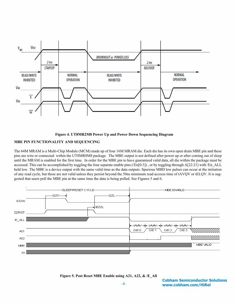
The MRAM is protected from write operations whenever VDD is less than VWI. As soon as VDD exceeds VDD(min), there is a startup time of 2 ms before read or write operations can start. This time allows memory power supplies to stabilize. The /En and /W control signals should track VDD on power up to VDD- 0.2 V or VIH (whichever is lower) and remain high for the startup time. In most systems, this means that these signals should be pulled up with a resistor so the signal remains high if the driving signal is Hi-Z during power up. Any logic that drives /En and /W should hold the signals high with a power-on reset signal for longer than the startup time. During power loss or brownout where VDD goes below VWI, writes are protected and a startup time must be observed when power returns above VDD(min).
The MRAM supports sleep/reset mode operation using the ZZ/RST control pin. To enter sleep mode/reset, ZZ/RST must be pulled high. The device will enter sleep/reset mode within 40ns. In order to exit sleep/reset mode, /En and /W must be high before ZZ/RST is pulled low. As soon as ZZ/RST is driven low, the user must allow 100us before performing any other operation in order for the device to properly initialize. Aeroflex recommends designing a system level method to toggle the ZZ/RST pin in order to reset the MRAM device.
Table 3. Device Operation Truth Table
ZZ/RST
/E[3:0]* /G /W Mode VDD Current
DQ[7:0]
H X X X Deep Sleep/Reset Mode
QIZZ HI-Z
L H X X Not Selected
QIDD
HI-Z
L L H H Output Disabled
IDDR HI-Z
L L L H Byte Read IDDR DOUT
L L X L Byte Write IDDW DINTable 4. Operational Environment
Design Specifications
PARAMETER LIMIT UNITS
TID 1 Mrad(Si)
SEL Immunity1 < 112 MeV-cm2/mg
SEU Memory Cell Immunity2
< 112 MeV-cm2/mg
*Note: Only one /E[3:0] pin may be active at any time.
Figure 4. UT8MR2M8 Power Up and Power Down Sequencing Diagram
Figure 5. Post Reset MBE Enable using A21, A22, & /E_All
MBE PIN FUNCTIONALITY AND SEQUENCING
The 64M MRAM is a Multi-Chip Module (MCM) made up of four 16M MRAM die. Each die has its own open drain MBE pin and thesepins are wire or connected within the UT8MR8M8 package. The MBE output is not defined after power up or after coming out of sleepuntil the MRAM is enabled for the first time. In order for the MBE pin to have guaranteed valid data, all die within the package must beaccessed. This can be accomplished by toggling the four separate enable pins (/En[0:3]) , or by toggling through A[22:21] with /En_ALLheld low. The MBE is a device output with the same valid time as the data outputs. Spurious MBD low pulses can occur at the initiationof any read cycle, but these are not valid unless they persist beyond the 50ns minimum read accesss time of tAVQV or tELQV. It is sug-gested that users poll the MBE pin at the same time the data is being polled. See Figures 5 and 6.
(Referenced to VSS) The device contains protection against magnetic fields. Precautions should be taken to avoid device exposure of any magnetic field intensity greater than specified.
Notes:1. Permanent device damage may occur if absolute maximum ratings are exceeded. Functional operation should be restricted to recommended operating conditions.
Exposure to excessive voltages or magnetic fields could affect device reliability.2. All voltages are referenced to VSS.3. Power dissipation capability depends on package characteristics and use environment
RECOMMENDED OPERATING CONDITIONS
Notes:1. After power up or if VDD falls below VWI, a waiting period of 2 ms must be observed, and /En and /W must remain high for 2 ms. Memory is designed to prevent writing for all input pin conditions if VDD falls below minimum VWI. 2. The MRAM is guaranteed to activate write inhibit below 2.5V, but may enter write inhibit mode anywhere within this voltage range. It is guaranteed to exit write inhibit mode once recommended operating voltage range is reached.
SYMBOL PARAMETER VALUE UNITVDD Supply Voltage2 -0.5 to 4.3 V
VIN Voltage on any pin2 -0.5 to VDD+0.5 V
IIO DC I/O current per pin @ TJ = 125° for 20yrs ± 20 mA
PD Package power dissipation3 4 W
TJ Maximum junction temperature +150 oC
JC Thermal resistance junction to case – Single Die 5 oC/WTSTG Storage temperature -65 to +125 oC
ESDHBM ESD >2000 V
H max_write Maximum magnetic field during write 8000 A/m
H max_read Maximum magnetic field during read or standby 8000 A/m
SYMBOL PARAMETER LIMITSTC Operating case temperature -40oC to +105oC
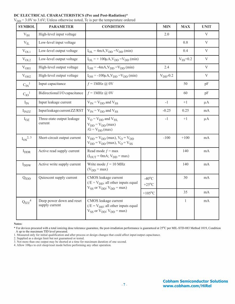
DC ELECTRICAL CHARACTERISTICS (Pre and Post-Radiation)*VDD = 3.0V to 3.6V; Unless otherwise noted, Tc is per the temperature ordered
Notes: * For devices procured with a total ionizing dose tolerance guarantee, the post-irradiation performance is guaranteed at 25oC per MIL-STD-883 Method 1019, Condition
A up to the maximum TID level procured. 1. Measured only for initial qualification and after process or design changes that could affect input/output capacitance.2. Supplied as a design limit but not guaranteed or tested.3. Not more than one output may be shorted at a time for maximum duration of one second.4. Allow 100s to exit sleep/reset mode before performing any other operation.
SYMBOL PARAMETER CONDITION MIN MAX UNIT
VIH High-level input voltage 2.0 V
VIL Low-level input voltage 0.8 V
VOL1 Low-level output voltage IOL = 4mA,VDD =VDD (min) 0.4 V
VOL2 Low-level output voltage IOL = + 100A,VDD =VDD (min) VSS+0.2 V
VOH1 High-level output voltage IOH = -4mA,VDD =VDD (min) 2.4 V
VOH2 High-level output voltage IOH = -100A,VDD =VDD (min) VDD-0.2 V
IIN Input leakage current VIN = VDD and VSS -1 +1 A
IINZZ Input leakage current ZZ/RST VIN = VDD and VSS -0.25 0.25 mA
IOZ Three-state output leakage current
VO = VDD and VSS, VDD = VDD (max) /G = VDD (max)
-1 +1 A
IOS2, 3 Short-circuit output current VDD = VDD (max), VO = VDD
VDD = VDD (max), VO = VSS
-100 +100 mA
IDDR Active read supply current Read mode ƒ = max(IOUT = 0mA; VDD = max)
140 mA
IDDW Active write supply current Write mode ƒ = 10 MHz(VDD = max)
140 mA
QIDD Quiescent supply current CMOS leakage current (/E = VDD; all other inputs equal VSS or VDD; VDD = max)
-40oC+25oC
30 mA
+105oC 35 mA
QIZZ4 Deep power down and reset
supply currentCMOS leakage current (/E = VDD; all other inputs equal VSS or VDD; VDD = max)
1 mA
AC CHARACTERISTICS READ CYCLE1 (Pre and Post-Radiation)*VDD = VDD (min); Unless otherwise noted, Tc is per the temperature ordered
Notes:* For devices procured with a total ionizing dose tolerance guarantee, the post-irradiation performance is guaranteed at 25oC per MIL-STD-883 Method 1019, Condition
A up to the maximum TID level procured.1. /W is high for read cycle. Power supplies must be properly grounded and decoupled, and bus contention conditions must be minimized or eliminated during read or
write cycles.2. Address valid before or at the same time /En goes low.3. tGLQVoutput enable valid time unless tAVAV or tAVQVhave not been satisfied.4. Transition is measured at +/-400mV from the steady-state voltage.
SYMBOL PARAMETER MIN MAX UNITtAVAV Read cycle time 50 ns
AC CHARACTERISTICS /W CONTROLLED WRITE CYCLE (Pre and Post-Radiation)*VDD= VDD (min); Unless otherwise noted, Tc is per the temperature ordered.
Notes:* For devices procured with a total ionizing dose tolerance guarantee, the post-irradiation performance is guaranteed at 25oC per MIL-STD-883 Method 1019, Condi-
tion A up to the maximum TID level procured.1. All write occurs during the overlap of /En low and /W low. Power supplies must be properly grounded and decoupled, and bus contention conditions must be mini-
mized or eliminated during read or write cycles. If /G goes low at the same time or after /W goes low, the output will remain in a high impedance state.2. All write cycle timings are referenced from the last valid address to the first transition address.3. Transition is measured +/-400mV from the steady-state voltage.
SYMBOL PARAMETER MIN MAX UNIT
tAVAV2 Write cycle time 50 ns
tAVWL Address set-up time 0 ns
tAVWH Address valid to end of write (/G high) 28 ns
tAVWH Address valid to end of write (/G low) 28 nstWLWHtWLEH
AC CHARACTERISTICS /En CONTROLLED WRITE CYCLE1 (Pre and Post-Radiation)*VDD= VDD (min); Unless otherwise noted, Tc is per the temperature ordered.
Notes:* For devices procured with a total ionizing dose tolerance guarantee, the post-irradiation performance is guaranteed at 25oC per MIL-STD-883 Method 1019, Con-
dition A up to the maximum TID level procured.1. All write occurs during the overlap of /En low and /W low. Power supplies must be properly grounded and decoupled, and bus contention conditions must be min-
imized or eliminated during read or write cycles. If /G goes low at the same time or after /W goes low, the output will remain in a high impedance state.2. All write cycle timings are referenced from the last valid address to the first transition address.3. If /En goes low at the same time or after /W goes low, the output will remain in a high-impedance state. If /En goes high at the same time or before /W goes high,
the output will remain in a high-impedance state.4. Transition is measured +/-400mV from the steady-state voltage.
SYMBOL PARAMETER MIN MAX UNIT
tAVAV2 Write cycle time 50 ns
tAVEL Address set-up time 0 ns
tAVEH Address valid to end of write (/G high) 28 ns
tAVEH Address valid to end of write (/G low) 28 ns
AC CHARACTERISTICS SLEEP/RESET MODE (Pre and Post-Radiation)*VDD= VDD (min); Unless otherwise noted, Tc is per the temperature ordered.
Notes:* For devices procured with a total ionizing dose tolerance guarantee, the post-irradiation performance is guaranteed at 25oC per MIL-STD-883 Method 1019, Con-
dition A up to the maximum TID level procured.1. /En and /W must be high for the entire time when ZZ/RST is pulled low in order to exit sleep/reset mode.2. ZZ/RST must be high for 40ns in order to enter sleep/reset mode.3. Parameters are supplied as a design limit, but are not tested nor guaranteed.
SYMBOL PARAMETER MIN MAX UNIT
tZZL1,3 Sleep/reset mode exit delay 100 s
tZZH2,3 Sleep/reset mode access time 50 ns
tEZZ3 Sleep/reset mode exit setup time 0 ns
tZZS3 Sleep/reset mode settle time
200 s
tEZZ
tZZLtZZH
IDDW
ZZ/RST
/E
/W
tZZS
Notes:1. Measurement of data output occurs at the low to high or high to low transition mid-point, typically, VDD/2.
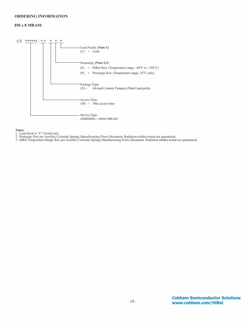
Package Type:(X) = 64-lead Ceramic Flatpack (50mil lead pitch)
Access Time:(50) = 50ns access time
Device Type:(8MR8M8) = 8Mx8 MRAM
Notes:1. Lead finish is "C" (Gold) only.2. Prototype flow per Aeroflex Colorado Springs Manufacturing Flows Document. Radiation neither tested nor guaranteed.3. HiRel Temperature Range flow per Aeroflex Colorado Springs Manufacturing Flows Document. Radiation neither tested nor guaranteed.
Class Designator:(Q) = QML Class Q (V) = QML Class V (pending contact factory)
Device Type (Note 2)(03) = 50ns access time. Temperature Range (-40C to +105C)(04) = 50ns access time (-40C to +105C) manufactured to QML-Q+ flow(02TBD)=15ns access time, CMOS I/O, 40-lead flatpack package, dual chip enable (not available)
Notes:1.Lead finish is "C" (Gold) only.2.Aeroflex’s Q+ flow, as defined in Section 4.2.2d of SMD, provides QML-Q product through the SMD that is manufactured with Aeroflex’s standard QML-V
The following United States (U.S.) Department of Commerce statement shall be applicable if these commod-ities, technology, or software are exported from the U.S.: These commodities, technology, or software were
C o b h a m C o l o r a d o S p r i n g s - D a t a s h e e t D e f i n i t i o n
A d v a n c e d D a t a s h e e t - P r o d u c t I n D e v e l o p m e n t
P r e l i m i n a r y D a t a s h e e t - S h i p p i n g P r o t o t y p e
D a t a s h e e t - S h i p p i n g Q M L & H i - R e l
Aeroflex Colorado Springs Inc., dba Cobham Semiconductor Solutions, reserves the right to make changes to any products and services described herein at any time without notice. Consult Aeroflex or an authorized sales representative to verify that the information in this data sheet is current before using this product. Aeroflex does not assume any responsibility or liability arising out of the application or use of any product or service described herein, except as expressly agreed to in writing by Aeroflex; nor does the purchase, lease, or use of a product or service from Aeroflex convey a license under any patent rights, copyrights, trademark rights, or any other of the intellectual rights of Aeroflex or of third parties.
Cobham Semiconductor Solutions4350 Centennial BlvdColorado Springs, CO 80907
January 2016 Added new Cobham datasheet template, QML V Achieved, added ZZ/RST description of internal pull-down, updated maximum junction temperature to 150C, changed unit from uA to mA for the IINZZ specification, and added MBE Functionality verbiage and diagrams.
All
November 2017
Removed (T) Prototype flow (Temperature range: -40 to +105C) as an ordering option. 14
July 2018 Added package weight. Edited Device Operation paragraph. Edited MBE Pin Functionality and Sequencing paragraph. Edited Recommended Operating Conditions VIH and added note 2.
1,2,4,6,12
Sept 2019 Marked QML V from page 1 features list as pending. Replaced device type 01 and 02 with 03 and 04 and noted QML V option on page 16 "pending contact factory". Added note 3. to page 7 for tGLQV clarification.Previous note 3 is now 4.