25
VLSI POWER ESTIMATION W A T MAHESH DANANJAYA
| Date post: | 18-Jul-2015 |
| Category: |
Technology |
| Upload: | mahesh-dananjaya |
| View: | 94 times |
| Download: | 3 times |

VLSI POWER ESTIMATIONW A T MAHESH DANANJAYA

POWER ESTIMATION
System Power
Dynamic Power
Switching Power Internal Power
Static power
Leakage Power

SWICTHING POWER
• Power generated due to output changes, thus
charging and discharging the load capacitance.
• Switching power dissipates mainly depend on the,
• System Clock Frequency
• Activity Switching Frequency
•Switching Power Calculation depends on the three factors
• 𝑪 − 𝑳𝒐𝒂𝒅 𝑪𝒂𝒑𝒂𝒄𝒊𝒕𝒂𝒏𝒄𝒆
• 𝒇 − 𝑺𝒘𝒊𝒕𝒄𝒉𝒊𝒏𝒈 𝑭𝒓𝒆𝒒𝒆𝒏𝒄𝒚
• 𝑽 − 𝑫𝒓𝒊𝒗𝒊𝒏𝒈 𝑽𝒐𝒍𝒕𝒂𝒈𝒆
𝑃𝑆 = 𝐶 ∗ 𝑉2 ∗ 𝑓
INTERNAL POWER
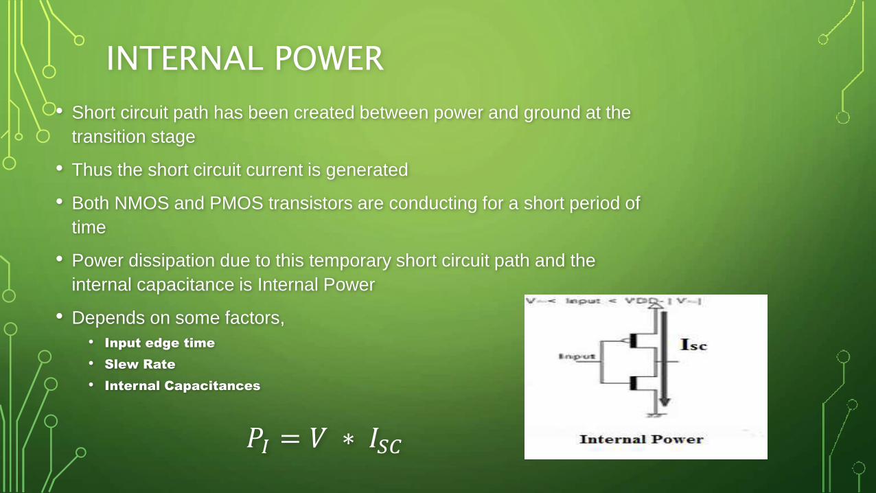
• Short circuit path has been created between power and ground at the
transition stage
• Thus the short circuit current is generated
• Both NMOS and PMOS transistors are conducting for a short period of
time
• Power dissipation due to this temporary short circuit path and the
internal capacitance is Internal Power
• Depends on some factors,
• Input edge time
• Slew Rate
• Internal Capacitances
𝑃𝐼 = 𝑉 ∗ 𝐼𝑆𝐶
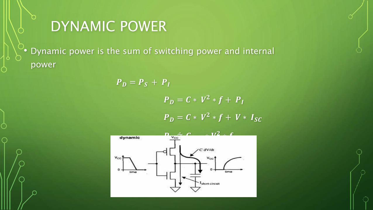
DYNAMIC POWER
• Dynamic power is the sum of switching power and internal
power
𝑷𝑫 = 𝑷𝑺 + 𝑷𝑰
𝑷𝑫 = 𝑪 ∗ 𝑽𝟐 ∗ 𝒇 + 𝑷𝑰
𝑷𝑫 = 𝑪 ∗ 𝑽𝟐 ∗ 𝒇 + 𝑽 ∗ 𝑰𝑺𝑪
𝑷𝑫 ⩭ 𝑪𝒆𝒇𝒇 ∗ 𝑽𝟐 ∗ 𝒇𝒔𝒘𝒊𝒕𝒄𝒉

STATIC POWER
• Due to non-idle characteristic of the transistor the
leakages can be taken place
• Static power is nothing, but leakage power
• There are two main types of leakages and their
subsidiaries
• 𝐼𝑂𝐹𝐹 − Sub-threshold leakage (Drain Leakage Current)
• 𝐼𝐷,𝑤𝑒𝑎𝑘 − 𝑆𝑢𝑏 − 𝑡ℎ𝑟𝑒𝑠ℎ𝑜𝑙𝑑 𝐷𝑟𝑎𝑖𝑛 𝐶𝑢𝑟𝑟𝑒𝑛𝑡
• 𝐼𝑖𝑛𝑣 − 𝑅𝑒𝑣𝑒𝑟𝑠𝑒 𝐵𝑖𝑎𝑠𝑒𝑑 𝐶𝑢𝑟𝑟𝑒𝑛𝑡
• 𝐼𝐺𝐼𝐷𝐿 − 𝐺𝑎𝑡𝑒 𝐼𝑛𝑑𝑢𝑐𝑒𝑑 𝐷𝑟𝑎𝑖𝑛 𝐿𝑒𝑎𝑘𝑎𝑔𝑒
• 𝐼𝐺𝐴𝑇𝐸 − Gate Leakage Current
• 𝐼𝑇𝑈𝑁𝑁𝐸𝐿 − 𝐺𝑎𝑡𝑒 𝑇𝑢𝑛𝑛𝑒𝑙𝑖𝑛𝑔
• 𝐼𝐻𝐶 − 𝐻𝑜𝑡 𝐶𝑎𝑟𝑟𝑖𝑒𝑟 𝐼𝑛𝑗𝑒𝑐𝑡𝑖𝑜𝑛

LEAKAGE POWER
𝐼𝐿𝐸𝐴𝐾𝐴𝐺𝐸
𝐼𝑂𝐹𝐹
𝐼𝐼𝑁𝑉 𝐼𝐷,𝑊𝐸𝐴𝐾 𝐼𝐺𝐼𝐷𝐿
𝐼𝐺𝐴𝑇𝐸
𝐼𝑇𝑈𝑁𝑁𝐸𝐿 𝐼𝐻𝐶

LEAKAGE POWER
𝑰𝑳𝑬𝑨𝑲𝑨𝑮𝑬 = 𝐼𝑂𝐹𝐹 + 𝐼𝐺𝐴𝑇𝐸
𝑷𝑺 = 𝑽 ∗ 𝑰𝒍𝒆𝒂𝒌
𝑰𝑮𝑨𝑻𝑬 = 𝐼𝐻𝐶 + 𝐼𝑇𝑈𝑁𝑁𝐸𝐿
𝑰𝑶𝑭𝑭 = 𝐼𝑖𝑛𝑣 + 𝐼𝐷,𝑤𝑒𝑎𝑘 + 𝐼𝐺𝐼𝐷𝐿

TRANSISTOR LEAKAGE MECHANISMS
• 𝐼𝑂𝐹𝐹 − 𝐷𝑟𝑎𝑖𝑛 𝐿𝑒𝑎𝑘𝑎𝑔𝑒 𝐶𝑢𝑟𝑟𝑒𝑛𝑡 – 𝑆𝑢𝑏 − 𝑡ℎ𝑟𝑒𝑠ℎ𝑜𝑙𝑑 𝐿𝑒𝑎𝑘𝑎𝑔𝑒 𝐶𝑢𝑟𝑟𝑒𝑛𝑡
(𝑓𝑙𝑜𝑤𝑠 𝑓𝑟𝑜𝑚 𝑑𝑟𝑎𝑖𝑛 𝑡𝑜 𝑠𝑜𝑢𝑟𝑐𝑒 𝑜𝑟 𝑏𝑜𝑑𝑦)
• 𝐼𝐷,𝑤𝑒𝑎𝑘 − 𝑆𝑢𝑏 − 𝑡ℎ𝑟𝑒𝑠ℎ𝑜𝑙𝑑 𝐷𝑟𝑎𝑖𝑛 𝐶𝑢𝑟𝑟𝑒𝑛𝑡
• 𝐼𝑖𝑛𝑣 − 𝑅𝑒𝑣𝑒𝑟𝑠𝑒 𝐵𝑖𝑎𝑠𝑒𝑑 𝐶𝑢𝑟𝑟𝑒𝑛𝑡
• 𝐼𝐺𝐼𝐷𝐿 − 𝐺𝑎𝑡𝑒 𝐼𝑛𝑑𝑢𝑐𝑒𝑑 𝐷𝑟𝑎𝑖𝑛 𝐿𝑒𝑎𝑘𝑎𝑔𝑒
• 𝐼𝐺𝐴𝑇𝐸 − 𝐺𝑎𝑡𝑒 𝐿𝑒𝑎𝑘𝑎𝑔𝑒 𝐶𝑢𝑟𝑟𝑒𝑛𝑡
(𝐿𝑒𝑎𝑘𝑎𝑔𝑒 𝑐𝑢𝑟𝑟𝑒𝑛𝑡 𝑡ℎ𝑎𝑡 𝑑𝑟𝑖𝑏𝑏𝑙𝑒 𝑡ℎ𝑟𝑜𝑢𝑔ℎ 𝑡ℎ𝑒 𝑔𝑎𝑡𝑒𝑠 𝑜𝑓 𝑡ℎ𝑒 𝑡𝑟𝑎𝑛𝑠𝑖𝑠𝑡𝑜𝑟)
• 𝐼𝑇𝑈𝑁𝑁𝐸𝐿 − 𝐺𝑎𝑡𝑒 𝑇𝑢𝑛𝑛𝑒𝑙𝑖𝑛𝑔
• 𝐼𝐻𝐶 − 𝐻𝑜𝑡 𝐶𝑎𝑟𝑟𝑖𝑒𝑟 𝐼𝑛𝑗𝑒𝑐𝑡𝑖𝑜𝑛

SUB-THRESHOLD LEAKAGE CURRENT (𝑰𝑶𝑭𝑭) • The sub-threshold leakage current of a transistor,𝐼𝑂𝐹𝐹, is
defined as the drain current when 𝑉𝑔 − 𝑉𝑠 = 0 and 𝑉𝐷 ≥ 0. 𝐼𝑂𝐹𝐹 is
dependent on the various factors such as,
• 𝑉𝐷𝐷 − 𝑆𝑢𝑝𝑝𝑙𝑦 𝑉𝑜𝑙𝑡𝑎𝑔𝑒
• 𝑉𝑡ℎ − 𝑇ℎ𝑟𝑒𝑠ℎ𝑜𝑙𝑑 𝑉𝑜𝑙𝑡𝑎𝑔𝑒
• Doping Concentration
• 𝑇𝑂𝑋 − 𝐺𝑎𝑡𝑒 𝑂𝑥𝑖𝑑𝑒 𝑇ℎ𝑖𝑛𝑒𝑠𝑠
• As we mentioned earlier 𝑰𝑶𝑭𝑭 is consist of 3 sub leakage
components.
• 𝐼𝐷,𝑤𝑒𝑎𝑘 − 𝑆𝑢𝑏 − 𝑡ℎ𝑟𝑒𝑠ℎ𝑜𝑙𝑑 𝐷𝑟𝑎𝑖𝑛 𝐶𝑢𝑟𝑟𝑒𝑛𝑡
• 𝐼𝑖𝑛𝑣 − 𝑅𝑒𝑣𝑒𝑟𝑠𝑒 𝐵𝑖𝑎𝑠𝑒𝑑 𝐶𝑢𝑟𝑟𝑒𝑛𝑡
• 𝐼𝐺𝐼𝐷𝐿 − 𝐺𝑎𝑡𝑒 𝐼𝑛𝑑𝑢𝑐𝑒𝑑 𝐷𝑟𝑎𝑖𝑛 𝐿𝑒𝑎𝑘𝑎𝑔𝑒
𝑰𝑶𝑭𝑭 = 𝐼𝑖𝑛𝑣 + 𝐼𝐷,𝑤𝑒𝑎𝑘 + 𝐼𝐺𝐼𝐷𝐿

𝑰𝒊𝒏𝒗 − 𝑹𝒆𝒗𝒆𝒓𝒔𝒆 𝑩𝒊𝒂𝒔𝒆𝒅 𝑪𝒖𝒓𝒓𝒆𝒏𝒕
• 𝑰𝒊𝒏𝒗 is the current that flows through the reverse biased diode
between the drain and the p region of the transistor, and it is
dependent on the junction area between the Source/Drain terminal
and the body and exponentially dependent to the temperature.
• Leakage current for the inverse biased diode can be modelled as
follows where,
• 𝑈𝑇 − 𝑇ℎ𝑒𝑟𝑚𝑎𝑙 𝑉𝑜𝑙𝑡𝑎𝑔𝑒 (𝑃𝑎𝑟𝑎𝑚𝑒𝑡𝑤𝑟 𝑙𝑖𝑛𝑒𝑎𝑟𝑙𝑦 𝑑𝑒𝑝𝑒𝑛𝑑𝑒𝑛𝑡 𝑜𝑛 𝑡ℎ𝑒 𝑣𝑜𝑙𝑡𝑎𝑔𝑒)
• 𝐼𝑆 − 𝑅𝑒𝑣𝑒𝑟𝑠𝑒 𝑆𝑎𝑡𝑢𝑟𝑎𝑡𝑖𝑜𝑛 𝐶𝑢𝑟𝑟𝑒𝑛𝑡 (𝐼𝑛𝑡𝑟𝑖𝑛𝑠𝑖𝑐 𝑃𝑎𝑟𝑎𝑚𝑒𝑡𝑒𝑟 𝑓𝑜𝑟 𝑡ℎ𝑒 𝑑𝑒𝑣𝑖𝑐𝑒)
• 𝑉𝐷 − 𝑉𝑜𝑙𝑡𝑎𝑔𝑒 𝑏𝑒𝑡𝑤𝑒𝑒𝑛 𝐷𝑟𝑎𝑖𝑛 𝑎𝑛𝑑 𝑡ℎ𝑒 𝐵𝑜𝑑𝑦𝑜𝑓 𝑡ℎ𝑒 𝑡𝑟𝑎𝑛𝑠𝑖𝑠𝑡𝑜𝑟
• 𝐽𝐼𝑁𝑉 − 𝑆𝑎𝑡𝑢𝑟𝑎𝑡𝑜𝑖𝑛 𝐶𝑢𝑟𝑟𝑒𝑛𝑡 𝐷𝑒𝑛𝑠𝑖𝑡𝑦
• 𝐴𝐷 − 𝐷𝑖𝑓𝑓𝑢𝑠𝑖𝑜𝑛 𝐴𝑟𝑒𝑎
𝑰𝑰𝑵𝑽 = 𝑰𝑺(𝒆 𝑽𝑫 𝑼𝑻 − 𝟏)
𝑰𝑰𝑵𝑽 = 𝑨𝑫 ∗ 𝑱𝑰𝑵𝑽

𝑰𝑫,𝒘𝒆𝒂𝒌 − SUB-THRESHOLD DRAIN CURRENT
• When,𝑉𝑔 < 𝑉𝑡ℎ , 𝑉𝑑 ≥ 0.1 𝑎𝑛𝑑 𝑉𝑠 = 𝑉𝑏 = 0, transistor forms a weak
inversion layer. Transistor in a weak inversion has a constant voltage
across the semiconductor channel and the longitudinal electric field across
the channel is null. Thus there is no drift current generating inside.
Instead the leakage current 𝑰𝑫,𝒘𝒆𝒂𝒌 is generated by the diffusion of
majority carriers across the channel. We can mathematically model this
sub-threshold drain leakage 𝑰𝑫,𝒘𝒆𝒂𝒌 with the following factors.
• 𝑈𝑇 − 𝑇ℎ𝑒𝑟𝑚𝑎𝑙 𝑉𝑜𝑙𝑡𝑎𝑔𝑒 (𝑃𝑎𝑟𝑎𝑚𝑒𝑡𝑤𝑟 𝑙𝑖𝑛𝑒𝑎𝑟𝑙𝑦 𝑑𝑒𝑝𝑒𝑛𝑑𝑒𝑛𝑡 𝑜𝑛 𝑡ℎ𝑒 𝑣𝑜𝑙𝑡𝑎𝑔𝑒)
• 𝑰𝟎 − 𝐼𝑛𝑖𝑡𝑖𝑎𝑙 𝐷𝐶 𝑜𝑓𝑓𝑠𝑒𝑡 𝑑𝑟𝑎𝑖𝑛 𝑐𝑢𝑟𝑟𝑒𝑛𝑡
• It is paramount important to look at the exponential dependency of 𝑰𝑫,𝒘𝒆𝒂𝒌
on 𝑉𝑔𝑠 as well as the linear offset based on 𝑉𝐷𝑆
𝑰𝑫,𝒘𝒆𝒂𝒌 =𝑾
𝑳× 𝑰𝟎 × 𝒆 𝑽𝒈𝒔− 𝑽𝒕𝒉 (𝒎 𝑼𝑻 )
−𝟏× (𝟏 − 𝒆−𝑽𝑫𝑺 ×𝒎×𝑼𝑻
−𝟏)

𝑰𝑮𝑰𝑫𝑳 − GATE INDUCED DRAIN LEAKAGE
• Gate-induced drain leakage is generated when a large
enough gate to drain 𝑉𝑔𝑑voltage is applied to produce a band to
band electron tunneling near the interface between the gate
oxide and the semiconductor of the drain.

𝑰𝑮𝑨𝑻𝑬 − GATE LEAKAGE
• The gate leakage current is dribbling across the gate to and
from the channel, substrate, and diffusion terminal.
• This current avoid the treatment of the gate of a device as an
ideally insulated electrode. This gate leakage is basically
composed of two leakage components.
• 𝐼𝑇𝑈𝑁𝑁𝐸𝐿 − 𝐺𝑎𝑡𝑒 𝑇𝑢𝑛𝑛𝑒𝑙𝑖𝑛𝑔
• 𝐼𝐻𝐶 − 𝐻𝑜𝑡 𝐶𝑎𝑟𝑟𝑖𝑒𝑟 𝐼𝑛𝑗𝑒𝑐𝑡𝑖𝑜𝑛
𝑰𝑻𝑼𝑵𝑵𝑬𝑳 − GATE TUNNELING
• This leakage current is generated due to carriers tunneling
through the gate of the transistor. There are two major
different way of carrier tunneling.
• Fowler-Nordheim Tunneling
Tunneling into the conduction band of the dielectric. It
manifest itself as electron emission caused by the intense high
electric field.
• Direct Tunneling
Tunneling to or from the gate through the forbidden band
gap of the dielectric

𝑰𝑯𝑪 − HOT CARRIER INJECTION
• This current is known as Hot Carrier Leakage which is
origin whenever a carrier gains enough kinetic energy and
overcome the gate potential barrier.
• This is more often happen to electrons since the voltage barrier
and effective mass of an electron is less than the one for holes.

VARIOUS OTHER POWER
• Metastability
• Output of the flops are remains on the undefined states which s caused
by the violation of setup time and hold time.
• Set Up Time
• Amount of time that the input signal needs to be stable before clocking the
flop
• Hold Time
• Amount of time that input signal wants to be stable after clocking the flop
• Glitches
• Glitches are unwanted or undesired changes in signals which are
resilient (self correcting).
• caused by delays in lines and propagation delays of cells.
• Latchups
• LatchUps is a short circuit path between supply and the ground

TECHNOLOGY SCALING AND POWER ESTIMATION • CMOS Device Scaling
• Gate Oxide Thickness (𝑻𝑶𝑿) Scaling
• Channel Miniaturization
• Supply Voltage and Threshold Voltage (𝑽𝒅𝒅 & 𝑽𝒕𝒉 ) Scaling
• Doping Concentration
• Source Drain Punchthrough
CMOS DEVICE SCALING
• Although the rate is slowing device scaling is slowing
down and deviating from the actual moor’s law, technology
sand device scaling is happening so rapidly. Therefore
designers have potential of inexpensive doubling the number
of transistors every two years, which is possible thank to the
miniaturization of devices and the reduction of the cost of
computer power due to sales volume. Therefore designers
have to be careful about the stuff because in near future the
transistor miniaturization reaches atomic level. Some
challenges still remain for the future
• Photolithography
• Manufacturing Cost
• Increased power density
• 𝐼 𝐼 current ratio

GATE OXIDE THICKNESS (𝑻𝑶𝑿) SCALING
• As long as semiconductor device is taking place, the gate oxide
thickness and effective channel length is getting reduced. This
thickness is one of the important parameter to FET and MOS devices
where it is directly engaging with the MOS capacitance and all that.
According to some papers the relationship of the 𝑻𝑶𝑿 scaling can be
illustrated as ,
𝐿𝑒𝑓𝑓 = 45 × 𝑇𝑂𝑋
𝐿𝑒𝑓𝑓 − 𝐸𝑓𝑓𝑒𝑐𝑡𝑖𝑣𝑒 𝐶ℎ𝑎𝑛𝑛𝑒𝑙 𝐿𝑒𝑛𝑔𝑡ℎ
• This relationship is usually leads to good 𝑉𝑔 − 𝐼𝑑transfer behavior.
With this device scaling and other restrictions, Gate Oxide Thickness
is limited to some typical level and create a barrier. There are two
leakage components which are affected by the 𝑻𝑶𝑿 scaling,
• 𝐼𝐺𝐼𝐷𝐿 − 𝐺𝑎𝑡𝑒 𝐼𝑛𝑑𝑢𝑐𝑒𝑑 𝐷𝑟𝑎𝑖𝑛 𝐿𝑒𝑎𝑘𝑎𝑔𝑒
• 𝐼𝑇𝑈𝑁𝑁𝐸𝐿 − 𝐺𝑎𝑡𝑒 𝐷𝑖𝑟𝑒𝑐𝑡 𝑇𝑢𝑛𝑛𝑒𝑙𝑖𝑛𝑔

CHANNEL MINIATURIZATION
As long as technology scaling happens the effective channel is
reducing and short-channel effects are expected to worsen when
channel length is reduced.
DIBL – Drain Induced Barrier Lowering is one such effect.
In DIBL scenario where depletion region of the source or drain
extends into the channel of a MOSFET device, effectively reducing the
channel length. This reduction in depletion layer lowers the potential
barrier for electrons, which results in an observable lowering of 𝑉𝑡ℎ,
and hence in an increase on the 𝑰𝑫,𝒘𝒆𝒂𝒌 current. And also channel
miniaturization reduces the junction area between the substrate and
the Source or Drain, effectively reducing the 𝑰𝒊𝒏𝒗. Channel
miniaturization is also closely related to scaling of the 𝑻𝑶𝑿 and
optimization is paramount importance for the best power

SUPPLY VOLTAGE AND THRESHOLD VOLTAGE (𝑽𝒅𝒅 & 𝑽𝒕𝒉 ) SCALING
• 𝑽𝒅𝒅 and 𝑽𝒕𝒉 are two vital transistor characteristics.
• Design engineers typically scale the supply voltage 𝑽𝒅𝒅 to
control dynamic power consumption and power density.
• In the same time reduction of 𝑽𝒅𝒅 forces a dramatic reduction
in Threshold voltage (𝑽𝒕𝒉) in order to raise the performance
gains.
• This reduction in 𝑽𝒕𝒉 typically causes a relatively large increase
in 𝑰𝑶𝑭𝑭, while the reduction of 𝑽𝒅𝒅 reduces the leakage current
substantially.
DOPING CONCENTRATION
• Electric field at a p-n junction strongly depends on the
junction doping. As long as technology and device scaling
continue, the doping concentration is rising, incrementing the
overall 𝑰𝒊𝒏𝒗 and 𝑰𝑻𝑼𝑵𝑵𝑬𝑳. Device engineers smart enough build a
smart doping profiles for the channel and the transistor
terminals to maximize active current driving through the
channel while minimizing the idle current.

SOURCE DRAIN PUNCHTHROUGH
• Punchthrough happens when the depletion regions from
the source and the drain join in the absence of a depletion
region induced by gate. Punchthrough happens when voltages
between the source and the body are above then nominal range
of 𝑉𝑑𝑑, since this is not the common case for digital circuits.
Therefore model punchthough is very important to ASIC
designers.

EDA POWER ESTIMATION
• Mostly based on the tech libraries
• Based on two major calculations
• Activity
• The number of toggles per clock cycle on the signal, averaged
over many cycles
• Probability
• Percentage of the time that the signal will be high


