Science and applications of Tailored Nanostructures 148 8 Welded metal nanowire networks for transparent electrode Force Tefo Thema 3,4 , Ishaq Ahmad 1,3,4* , Javed Iqbal 2,3,4 and Malik Maaza 3,4 1 National Center for Physics, Quaid-i-Azam University, Islamabad, Pakistan 2 Physics Department, Quaid-i-Azam University, Islamabad, Pakistan 3 UNESCO-UNISA Africa Chair in Nanosciences/Nanotechnology, University of South Africa, Pretoria-South Africa. Nanosciences African Network (NANOAFNET), iThemba LABS-NRA, South Africa * Corresponding author Outline Introduction…………….…………….…………….…………….…………….…………….…………….…………….……………… 149 Joule Heat Welding ………………………………………………………………………………………………………………….…. 150 Plasmonic welding............................................................................................................................ 154 Gamma-rays irradiation induced welding……………………………………………………………………................. 155 Cold Welding……………………………………………………………....................................................……............ 158 Ion irradiation induced welding………………………………………………………………………………………..……...... 160 Electron Beam welding...................................................................................................……............ 165 Conclusion………………………………………………………………………………………………………………………………….. 167 References………………………………………………………………………………………………………………………………….. 167
Transcript
Science and applications of Tailored Nanostructures 148 148
8 Welded metal nanowire networks for transparent electrode
Force Tefo Thema
3,4, Ishaq Ahmad
1,3,4*, Javed Iqbal
2,3,4 and Malik Maaza
3,4
1National Center for Physics, Quaid-i-Azam University, Islamabad, Pakistan 2Physics Department, Quaid-i-Azam University, Islamabad, Pakistan 3UNESCO-UNISA Africa Chair in Nanosciences/Nanotechnology, University of South Africa, Pretoria-South Africa. Nanosciences African Network (NANOAFNET), iThemba LABS-NRA, South Africa *Corresponding author
Science and applications of Tailored Nanostructures 149 149
Introduction This chapter introduces the reader to the welding techniques of metal nanowires (NWs) to fabricate large area welded networks for transparent electrodes. Post-processing welding techniques to assemble metal NWs into large area network may be useful process to enhance the electrical conductivity and transparency of transparent electrodes that are much required. Generally, transparent electrodes have vast applications in optoelectronics such as thin-film solar cells, liquid crystal displays and smart windows. These electrodes provide platform for more photons to pass through a substantial part of the optoelectronic device surface [1]. Recently, metal oxides such as Al-doped zinc oxide and indium tin oxide (ITO) have been widely used as transparent conductive electrodes for optoelectronics applications. However, these electrodes are not suitable for some optoelectronic devices such as flexible solar cells, organic light emitting diodes etc. Since metal oxides have brittle behavior in nature when making metal oxides based devices, electrodes cracking occurs on thin film resulting into the system failure [2]. Therefore, search for alternate transparent conductive flexible materials is imperative for flexible electronics devices and optoelectronic devices [3, 4]. To achieve this goal, various alternatives materials have been scrutinized by different researchers, among which thin metal films [5] and metal grids [6] have shown better performance compared to ITO. However, these approaches require processing and fabrication using high vacuum equipment and resulting Transparent Conducting Electrodes (TCE) show the limited bending ability. Carbon nanotubes films and graphene films have also been studied for this purpose and have attracted significant attention for their use as TCEs in optoelectronic devices [7]. However, their performance in terms of optical transparency and sheet resistance is still inferior to ITO, creating a need to continue the quest for new materials which can act as cheap and reliable TCEs [3]. Recently, other pioneering approaches have also been reported including conductive polymers [8], nanowires [9-12], and metal mesh structures [1]. Among these alternatives, network of one dimensional metal nanowire especially silver and copper nanowires have been considered as a promising candidate for the next generation transparent electrodes due to their high electrical conductivity, high mechanical flexibility, and high optical transparency [13]. In order to exploit the exceptional properties of metal nanowires for application as a transparent electrode, improvement of optical transmission along with electrical conductivity is always required [14]. It is therefore, imperative to find a suitable method that not only improves electrical conductivity but also enhances transparency simultaneously using post treatment methods [13-17]. Different methods were adopted to fabricate highly transparent metal nanowires thin films resulting in improved electrical conductivity [17-21]. Metal nanowires provide a good percolation path for electrons to flow through, but it is hard to enhance electrical conductivity of transparent based metal nanowires electrodes because of junction resistance between metal nanowires at the contact point. Therefore, fabrication processing is required to reduce nanowires-nanowires resistance to finally optimize network conductivity. Junctions are the basic building blocks of any nanowires network. To reduce junction resistance, it is therefore, possible to get highly conductive nanowires network. There are different ways to reduce junction resistance between nanowires. One of the best methods is to weld metal nanowires and reduce the junction’s resistance. Therefore, welding the metal nanowire junction is an effective strategy for reducing the sheet resistance and improving the operational stability of metal nanowires electrodes in practical applications. Scientists have discovered a way to link nanowires into complex nanostructures and circuits by fusing different welding methods. The process is a new form of nano welding. The new technique may address an ongoing problem in nanotechnology research.
Science and applications of Tailored Nanostructures 150 150
There are many methods to weld metal nanowires such as Joule heating, cold welding, thermal sintering, electron beam induced welding, plasmonic welding, soldering, mechanical bonding and focused ion beam welding. Some welding methods are suitable to make large area welded metal nanowires network for transparent electrodes and some are not suitable for such applications. For example, focused electron beam or focused ion beam induced fusion welding. In this method, focused electron beam from scanning electron microscopy (SEM) is used as a heating source to fuse nanowires at the contact point. Basically, when focused electron beam hits nanowires, electrons lose kinetic energy due to inelastic scattering caused by localized heat dissipation into metal nanowires. This localized heating effect is used to diffuse metal nanowires at junction points hence welding occur. The drawback of this technique is that it takes a long time to focus electron beam in every part of the junctions and weld them to make large area network for transparent electrodes. Transparent electrodes have hundreds of junction’s points and making an electron focus on each one of them is hectic. Moreover, the structure and morphology change after intense focused electron beam induced fusion welding. While broad beam of electron could be used to weld metal nanowires to form welded network for transparent electrodes. Broad beam welding by electron will be discussed later in this chapter. Similarly, hot press welding is another method to weld metal nanowires but its drawback is that mostly nanowires could be damaged. At the same time, it is slightly hard to use hot press welding method to any flexible polymer substrates for fabricating flexible conductive transparent electrodes. In addition, focused ion beam technique which is now used for welding of nano object and as well as for lithography is also not suitable for fabricating large area welded network for transparent electrodes. Because in this method which is similar to electron beam needs to focus each part of junctions points with focus ion beam and then due to ion beam induced local heating with collision cascade effects, nanowires at the junction points fused on each other get perfect nano-welding. For large area network it will take a long time to weld all the junctions. Therefore, this method is also not suitable for large area welded network of metal nanowires. But is perfect method to integrate nanodevice. In spite of above welding methods of metal nanowires, we herein, now able to discuss feasible methods to make large area welded network of metal nanowires for transparent electrodes. These methods are mainly intended for large scale nanowire meshes. Each method has its own advantages and disadvantages. Here in this book chapter, different welding approaches such as cold welding, Joule heating, will be discussed in detail to reduce the junction resistance of metal nanowires network. Furthermore, we will also discuss each welding method in detail and its advantages and disadvantages.
Joule heat welding Joules heat welding is a versatile technique to weld from large metal objects to nanometer scale metal objects. This is a simple technique to weld metal nanowires and finally get welded network of metal nanowires for transparent electrodes. Moreover, this welding technique may be used in nanodevice manufacturing industry for joining and integrating nanodevice components. In this technique, current flows through the metal nanowire network which leads to heating. The heating then melts nanowires at contact position to form welded network of metal nanowires. Joule heating experimental setup is shown in Figure 8.1. In this figure, a white colored random dispersed unwelded metal nanowires network is fabricated on any substrate using different
Science and applications of Tailored Nanostructures 151 151
techniques such as spray coating, spin coating or direct synthesis method. The electrical contacting points to the metal nanowires must be formed to flow current for Joule heating. Different procedures could be adopted to make metal contact like e-beam lithography, thermal evaporation and electron beam evaporation etc. Controlled DC source is connected across two electrodes and a direct current bias could be initiated between the electrodes in order to allow current flows through the unwelded metal nanowires network electrode. In this method, current limit should be availed and fixed through computer controlled direct current power supply to avoid high current breakdown of the network.
FIGURE 8.1 Joules heating experimental setup
Let constant current flow by computer controlled direct current power supply through unwelded metal nanowires network by connecting cables with electrodes as shown in Figure 8.2. During current flow through the metal nanowires network, the rate of generating heat is equal to q = I
2 R
where R is the electrical resistance of the entire metal nanowire and is given by ρx/A where ρ is electrical resistivity of the nanowires network and A is the cross sectional area of the nanowire. The R value at the junction point between the nanowire is very high as compared to the actual area between the contact point which is smaller than A. Therefore, q between the junction points of the nanowires is greater than the entire nanowire and this increases local temperature at contact point of metal nanowires which cause melting locally by current flow. Due to current flow induced, metal nanowires melt and fuse on each other at the contact points and get welded together forming networks as shown by red colored spots on the metal nanowires in Figure 8.2. After melting nanowires, the cross sectional area increases and this reduces resistance hence decreasing joule heating and causing solidification of metal nanowire contact region. Joules heating welding of nanowires can be done simply by adjusting and controlling the time it takes and the amount of the supplied current respectively. This constant current joule heating process is only possible with highly fabricated conductive metal nanowires network without pretreated welding method. There is no dielectric materials existence between nanowires junction points. For instance, if metal based electrodes were having high resistance between metal nanowires due to residual organic compounds like polyvinyl polymer (PVP), or because of photoresist which results from the fabrication and synthesis process and the metal nanowires exhibiting corrosion due to oxidation in air. Then, there is need for two steps joules heating process. In two step welding process we need both current source and voltage source to avoid
Science and applications of Tailored Nanostructures 152 152
damaging nanowires during welding process. During this two-step method, initially, voltage source applied between two electrodes reduces contact resistance due to dielectric coating of nanowires. Then a current flow through the metal nanowire network leads to heating. The heating and then melts nanowires at contact position form welded network of metal nanowires. Firstly, using a voltage ramp, the potential difference at the junction is increased until the dielectric barrier is ruptured causing current increase. The surge voltage is faster and double by simply using a ramp function. Without necessarily having to incrementally adjusting a constant voltage frequently this ultimately changes surge voltage.
FIGURE 8.2 Welded network by Joules heating
To prevent damage metal nanowires at the junction points, current should be limited through computer control power supply. At each point in time the ‘surge voltage’ is reached, heat produced which breaks dielectric materials layer reducing contact resistance. Repeating the voltage ramp will then lead to the increase in the slope of the current voltage curve because of low contact resistance hence the current surge is realizable at lower voltages. The ramping process occurs frequently such that resistance becomes so low and forced current cannot automatically damage or cause any defects on the nanowires. After reducing resistance between contact points of the nanowires, current source method can be utilized for further controlled welding of metal nanowires as previously discussed. Arash vafaei et al. used two step method to weld Ag-NWs successfully as shown in Figure 8.3 [18].
Science and applications of Tailored Nanostructures 153 153
FIGURE 8.3 (a) Voltage sweeps to reduce resistance at the contacts points of metal nanowires until the dielectric barrier is ruptured causing current increase. (b) Current ramp sweeps decrease contact resistance and heats up and starts welding. (c) SEM image of Ag nanowires welding after two step welding process [18]
Tohmyoh H. et al. used current source method to weld metal nanowires [19]. A constant current was applied to the system, where the free ends of two Pt nanowires were in contact. The ends were welded together successfully to result in a continuous straight wire as shown in Figure 8.4. Similarly, Song et al, used joule heating method and successfully got silver nanowires network [20].
FIGURE 8.4 Welded Pt nanowires a) straight welding, b) lap welding [19]
Science and applications of Tailored Nanostructures 154 154
Plasmonic welding Plasmonic nanowelding is another promising new metal nanowire welding technique that just uses ordinary light to create Plasmon. Here, the particles of oscillating plasma that are created when the light strikes a metal surface fuse the nanowires at the junction points. When light interacts with metal, it flows across the surface of the metal in the form of waves called plasmonic wave like water wave. When two metal nanowires placed on each other, the light will generate Plasmon waves at the junction points of metal nanowires which create a hot spot and finally form good welding between the nanowires. The beauty of this method is that when light is exposed the hot spots are only created where the nanowires touch each other causing welding. After welding there is no hot spot created. The welding automatically stops and this is due to its self-limiting natural behavior. Each top nanowire acts like an antenna, guiding the Plasmon waves into the wire beneath it. This creates heat which causes the two nanowires to fuse together where they touch each other. The process does not affect the rest of the nanowires or the underlying material. This method cannot only be used to produce nanowire network easily, but can also be utilized handily to create network electrodes for flexible and transparent surfaces. Figure 8.5 shows the plasmonic nanowelding experimental setup. First unwelded network can be fabricated on any substrate by using different techniques such as spray coating and spin coating method. Herein, in this setup Silver (Ag) nanowires were spray coated on glass substrate as shown in Figure 8.5a. This Figure clearly shows that Ag nanowires are unwelded. A tungsten halogen lamps which has wide range of radiation output from ultra violet to infrared region with a temperature of 3,050 K [21] could be used to illuminate unwelded metal nanowire networks. When a lamp generates light of about illumination power density of about 30 W/cm
2 interacts with metal
nanowires, plasmonic waves are then generated at a place where the two nanowires have small gaps between the upper and lower Ag nanowires; these gaps enable extreme local heating due to the optical radiation coupling with plasmonic modes and creates hot spots as shown in Figure 8.5b as red spots. Red spot creates heat at junction points then Ag nanowires fuse on each other which increased contact area. Ag nanowires welded network are then achieved using plasmonic welding. The SEM image clearly shows that Ag nanowires are welded perfectly as shown in Figure 8.5c. From plasmonic welding, highly conductive and transparent welded metal nanowires network can be possible. This method is suitable for large scale and highly conductive transparent flexible electrodes. As per experimental work, the Ag nanowires were deposited on a surface randomly by spraying. This resulted in many of the nanowires lying over one another in a crisscross pattern. Due to the insulating layer where the nanowires cross, a gap in nanometer range exists between them. Basically, when Plasmonic light passes onto the scattered nanowires, heat is generated at these gaps causing the silver to melt and fuse the nanowires together. This highly localized heating arises from the extreme field enhancements in small gaps between metal nanoparticles and is well known in the field of Plasmonic. The oscillating electric field of the light drives free electrons in the metal to move back and forth and heat up rapidly. This happens slightly everywhere along the nanowire but is very intense near the junction due to the high local fields which cause strong heating and ultimate nanowelding. Advantage of plasmonic welding is that metal nanowires can be welded at room temperature and it is a fast process compared to other methods. Therefore, this method is more effective on heat sensitive, flexible and stretchable substrates [22]. Similar ideas were taken by different scientists using laser source with fixed frequency as a light source to weld metal nanowires using plasmonic concept [22].
Science and applications of Tailored Nanostructures 155 155
-irradiations induced nano-welding is another welding approach to weld metal nanowires to form
large area welded network for transparent electrodes. In this approach, optimized dose of (Gamma) exposure is required to weld metal nanowires. This method is reported for the first time here in this book and explained with experimental work on Cu-nanowires. To get complete welding of nanowires the following steps may be considered.
a) Necking of nanowires b) Joining of nanowire c) Coalescence of nanowires
To get above steps the following experimental parameters need to be explored and finally optimized. In our experiments we optimized the following parameters and got complete welded network of Cu-nanowires.
a) -photons source: Co60
b) -photons Energy: 5 MeV c) Exposure environment: Room Temperature and atmospheric pressure d) Dose rate: 38Gy/min e) Dose for necking Cu-nanowire: 6 kGy f) Dose for joining Cu-nanowires: 9 kGy g) Dose for coalescence Cu-nanowires: 15 kGy
In this experiment un-irradiated Cu-nanowires network as shown in Figure 8.6 is irradiated with γ- irradiation to a dose of 6 kGy and observed that coalescence of these nanowires is started and it is called necking as shown in Figure 8.6c. Where figure 8.6b is the corresponding EDX of un-irradiated Cu-nanowires.
Science and applications of Tailored Nanostructures 156 156
FIGURE 8.6 SEM images of Cu-NWs (a) un-irradiated and (b) corresponding EDX spectra, (c) Irradiated at 6 kGy ions/cm
2
[42]
Further increase in γ-dose up to 9 kGy resulted in nano-welding between two Cu-nanowire and formed different shapes of junctions by coalescence of Cu nanowires (Figure 8.7). γ-radiation induced coalescence occurs when molecular bonding of metal nanowires is broken then spacing between atoms decreases and does re-bonding.
Science and applications of Tailored Nanostructures 157 157
FIGURE 8.7 SEM image of γ- irradiated Cu nanowires at a dose of 9 kGy: different type of junctions formed Y-, II-shape etc. [42]
Further increase in γ- irradiation dose up to 15 kGy coalescence between Cu-nanowires occurs at junction points resulting in welding of Cu-nanowires as shown in Figure 8.8.
FIGURE 8.8 SEM image of γ- irradiated Cu-NWs at the dose of 15 kGy [42]
Science and applications of Tailored Nanostructures 158 158
In this welding method, basically, γ–rays irradiation breaks Cu-Cu bonds of Cu-nanowires isotropically and making these bonds again forming junctions, which ultimately resulted in welded Cu-nanowires networks. However, the morphology and structure of the nanowires remained unchanged. Finally, Cu-nanowires form different types of molecular junctions. The breakage of Cu-nanowires was conducted using the γ- irradiation that acted only on the covalent bonds leaving the structure intact. γ-irradiation in MeV energy range interacted with target material and suffers significant electronic energy loss along their paths in the target material. Schematic mechanism of the welding process is presented in Figure 8.9 where the process is started from necking to joining of Cu-nanowires when subjected to medium γ-fluence and finally to complete coalescence of two nanowires at high γ-fluence, forming single nanowires with double diameter. γ- Irradiation induced nano-welding of Cu-nanowires is a new approach to integrate any nanodevice or forming welded networks for solar cells. The welding of Ag-nanowires has matured for fabrication of transparent electrodes for solar cells while work on welded networks of Cu-nanowires as a transparent electrode still needs to be explored. Our new approach to get welded conducting networks of Cu-nanowires will be useful for solar cell designers and integration of nanodevice.
FIGURE 8.9 Gamma irradiation induced welding process
It is concluded that a gamma irradiation induced nano welding technique is another approach to weld metal nanowires and could be possible to fabricate large area welded network of metal nanowires for conductive transparent electrodes using γ- irradiation technique.
Cold welding Welding of metal nanowires using cold welding is another promising technique to be used for welding of metal nanowires to make highly conductive, flexible and transparent electrodes [23]. This method is a solid phase technique by which pressure at room temperature ignites coalescence
Science and applications of Tailored Nanostructures 159 159
process between two metals. The pressure produced causes deformation to reach a desired state. Cold welding technique is designed for softer metals such as aluminum, copper, silver, nickel, magnesium, iron and materials like plastic and resins. The most frequently used application by this method is with binary composites like aluminum (Al) and with dissimilar metals such as aluminum-copper (Al-Cu). It is also widely used in the electrical engineering and aviation industry just to mention a few. Currently this technique is now used broadly in the nanoscale regime to weld metal nanowires for interconnection of devices to fabricate highly conductive transparent electrodes. During this process, the welding naturally happens due to the interaction of atomic attractive forces between the two individual nanowires in contact upon pressure. After cold press of metal nanowires network, the nanowires at contact position press tightly forming welded junction without loss of crystal structure. This type of welded network has high conductivity and mechanical strength. Consequently, this process is suitable where heat has to be avoided, for example to make flexible transparent electrodes on organic substrates where cold welding is ideal to improve conductivity without any loss of transparency. Cold press experimental setup is shown in Figure 8.10. In this figure a random dispersed unwelded network is fabricated on any substrate using different techniques such as spray coating, and spin coating method. These networks have less conductivity. To increase conductivity cold pressing is used. Any metal nanowire coated transparent substrate especially plastic substrates are put on the substrate holder and upper part moved toward the film and pressed at MPa range. When pressure is increased, metal nanowires start to diffuse into each other to cause coalescence at contact points capable of providing strong and high purity joints by merging and forming welded network with increased conductivity. In this process, the nanowires at contact position press tightly forming welded junction without loss of crystal structure. This type of welded network has highly conductive and mechanical strength. Advantage of this method is that junctions between metal NWs were mechanically compressed while maintaining the width of the metal NWs as shown in Figure 8.10. Another advantage is that cold press welding improves the surface roughness which increases surface area and hence improves conductivity. Yang Lu et al, successfully applied cold welding method and nicely welded Gold nanowires [23]. By mechanical contact and relatively low applied pressure, this method proved to be ideal and suitable for welding metal nanowires. In addition, T Tokuno et al used cold press method and he successfully fabricated transparent Ag-nanowires electrodes [24]. He used 25 MPa pressure for 5 seconds at room temperature to fabricate Ag-nanowires welded network. Electrical conductivity was measured and had improved with transparency of network at 80% [24]. It is therefore, concluded that this method is suitable in heat sensitive substrates.
Science and applications of Tailored Nanostructures 160 160
FIGURE 8.10 Schematic diagram of cold welding process
Ion irradiation induced welding
A fundamentally unique idea was recently observed when multiwalled carbon nanotubes (MWCNTs) were irradiated and finally got large scale welded network of MWCNTs [25]. It was demonstrated that welding between MWNT’s can be formed together with ion beam combined with high temperature annealing using Ar ions [26]. In ion beam irradiation welding process, MWCNTs were irradiated with Ar ions under high temperature of 800 K. Welding is possible due to Ar ion beam irradiation induced defects, vacancies and interstitials creation. At the same time and under high temperature, these defects recombined through interstitial atom migration and dangling bond saturation giving rise to the formation of intertube covalent bonds forming common graphene. This eventually formed junctions as shown in Figure 8.11 [26]. The HRTEM images of Figure 8.11 a and 8.11 b show the perfect welding of MWCNTs using Ar ion beam irradiation at the dose of 5 x10
16 ions/cm
2 and substrate temperature of 800 K. Moreover, different types of
junctions formed Y or X or II-shape like junctions. The Y and II-shape junctions between MWCNTs formed by Ar ions irradiation under elevated temperature showing common graphene are shown in Fig 8.11 a, 11b. Parallel and Y-shape junctions are also observed. It should be explained that ion beam induced self-organized process in which carbon atoms sputtered and agglomerated. At the same time there was disorder created in the graphene layers but reorganized by higher temperature annealing [26]. While cross junctions are formed by sputtering amorphous carbon, which was agglomerated at the cross position of two MWCNTs as shown in Figure 8.11c, all these type of junctions then combined at a same type forming large scale welded network as shown in figure 8.11d.
Science and applications of Tailored Nanostructures 161 161
Ion beam irradiation welding could be ascribed to ion beam produced defects in the crystal lattice due to collision cascade effects and sputtering of atoms from nanowires/nanotubes as well as ion beam induced local heating. At the same time, annealing at higher temperature gives rise to drop defects due to recombination of defects. During recombination of defects process, the dangling bonds of the carbon atoms at the contact points between MWCNTs can serve as bridges to form inter-tube covalent bonds forming welded junctions. The beauty of this method is that at heating condition, amorphization process by ion beam irradiation greatly decreased. It means heating prevents the MWCNTs into amorphous structure. Furthermore, using combined ion irradiation and annealing we got large area welded network of MWCNTs and found enhanced electrical and optical properties of these network as shown in figure 8.11 d. It is concluded that ion beam irradiation is another approach to weld metal nanowires to form welded network for transparent electrode.
FIGURE 8.11 HRTEM images (a) Y-shape welding of MWCNTs, (b) parallel-shape welding of MWCNTs (c) Cross shape welding of MWCNTs, TEM image of large scale welded network of MWCNTs. Welding were performed under 70 KeV Ar ion irradiation at the dose of 4 x 10
16 ions/cm
2 at the temperature of 800 K [26]
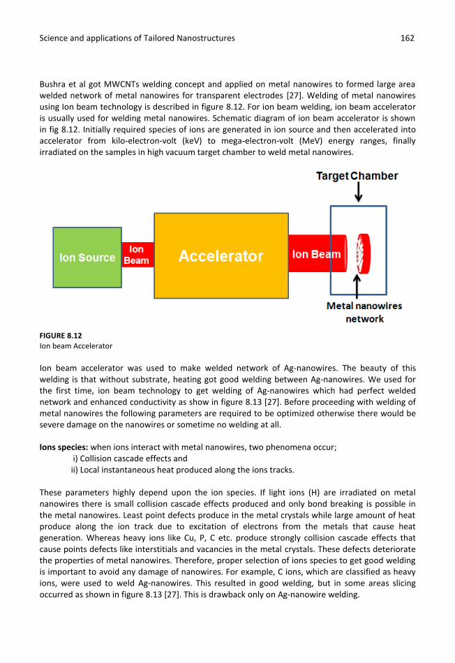
Science and applications of Tailored Nanostructures 162 162
Bushra et al got MWCNTs welding concept and applied on metal nanowires to formed large area welded network of metal nanowires for transparent electrodes [27]. Welding of metal nanowires using Ion beam technology is described in figure 8.12. For ion beam welding, ion beam accelerator is usually used for welding metal nanowires. Schematic diagram of ion beam accelerator is shown in fig 8.12. Initially required species of ions are generated in ion source and then accelerated into accelerator from kilo-electron-volt (keV) to mega-electron-volt (MeV) energy ranges, finally irradiated on the samples in high vacuum target chamber to weld metal nanowires.
FIGURE 8.12 Ion beam Accelerator
Ion beam accelerator was used to make welded network of Ag-nanowires. The beauty of this welding is that without substrate, heating got good welding between Ag-nanowires. We used for the first time, ion beam technology to get welding of Ag-nanowires which had perfect welded network and enhanced conductivity as show in figure 8.13 [27]. Before proceeding with welding of metal nanowires the following parameters are required to be optimized otherwise there would be severe damage on the nanowires or sometime no welding at all.
Ions species: when ions interact with metal nanowires, two phenomena occur; i) Collision cascade effects and
ii) Local instantaneous heat produced along the ions tracks. These parameters highly depend upon the ion species. If light ions (H) are irradiated on metal nanowires there is small collision cascade effects produced and only bond breaking is possible in the metal nanowires. Least point defects produce in the metal crystals while large amount of heat produce along the ion track due to excitation of electrons from the metals that cause heat generation. Whereas heavy ions like Cu, P, C etc. produce strongly collision cascade effects that cause points defects like interstitials and vacancies in the metal crystals. These defects deteriorate the properties of metal nanowires. Therefore, proper selection of ions species to get good welding is important to avoid any damage of nanowires. For example, C ions, which are classified as heavy ions, were used to weld Ag-nanowires. This resulted in good welding, but in some areas slicing occurred as shown in figure 8.13 [27]. This is drawback only on Ag-nanowire welding.
Science and applications of Tailored Nanostructures 163 163
FIGURE 8.13 SEM image (a) welded network of Ag nanowires and (b) corresponding HRSEM images of welded cross- and Y-shape junctions, at a dose of 2 x 10
15 ions/cm
2 [27]
Whereas, when light ions like proton are used, we get good network that has good transparency and conductivity [28, 29] as shown in figure 8.14. Figure 8.13 and 8.14, which clearly show the difference between ion species.
FIGURE 8.14 SEM images (a) Un-irradiated, (b) welded network of Ag nanowires and (c-e) corresponding HRSEM images of welded junctions irradiated at 4 × 10
15 protons /cm
2 [28]
Science and applications of Tailored Nanostructures 164 164
Optimum ions energy: Optimum ion energy means that ions species should have enough energy to pass through the two nanowires at contact points to initiates diffusion between the two nanowires. This allows ion species to penetrate through the upper metal nanowire and displace some atoms of the lower nanowires due to ion beam induced collision cascade effects that may cause ion beam induced diffusion of nanowires as shown in Figure 8.15. Or bond breaking at the interface between metal nanowires to make strong bonding between two nanowires to make good electrical contact. Therefore, optimum energy is always required to weld metal nanowires perfectly.
FIGURE 8.15 ion beam induced diffusion of nanowires
Optimum ions dose: This is another parameter that needs to be optimized for perfect welding of metal nanowires. For perfect welding it should be considered how much atoms need to be displaced for diffusion process of metal nanowires at the contact point and also how much bonds need to be broken to make good contact between nanowires. All that depends upon the ion doses. Therefore, for good electrical contact, dose should be optimized. For instant, at the dose of 1x10
16
under carbon ions irradiation, whole network welded but severely damaged where ultimate conductivity was reduced as shown in Figure 8.16 [27]. For perfect welded Ag-nanowires network, carbon ion dose of 4 × 10
15 protons /cm
2 is the optimized dose as shown previously (figure 8.14).
Below or higher doses cannot result into perfect Ag-nanowires welding.
FIGURE 8.16 SEM image (a) welded network of Ag nanowires and corresponding HRSEM images of showing thinning and slicing of Ag nanowires at a dose of 2 x 10
15 Carbon ions/cm
2 [27]
Science and applications of Tailored Nanostructures 165 165
Optimum ions current: This parameter is also important in the sense that ions produce heat along the track of nanowires. If ion current is too high then too much heat will be produced which may defuse nanowires together at contact points or sometimes damage nanowires due to heat induced evaporation. Therefore, controlling ion current can influence welding of metal nanowires. All above irradiation parameters are important and need to be considered when designing experiment to make highly conductive and transparent electrodes. Disadvantage of this method is that substrate may slightly deteriorate their properties. Overall, this is a good technique to make highly conductive transparent electrodes and is also useful for welding individual nanowires/nanowires through focus ion beam to integrate nanodevice.
Electron beam welding Besides other spontaneous heating sources to diffuse metal nanowires at junction points, energetic electron beam could be used to weld metal nanowires and ultimately get welded network of metal nanowires for transparent electrodes. In our previous study, we indicated that energetic electron beam could be used to pattern nanowires [30]. In this experiment, we used electron beam from transmission electron microscopy (TEM) and focused it on ZnO nanowires to create holes and cut nanowires as show in Figure 8.17. This experiment shows that electron beam produces local heating which leads to evaporation or sputtering of materials from the nanowires and ultimately make a pattern in nanoscale level. This experiment shows that electron beam also produce localized heat and may be used for welding of metal nanowires.
FIGURE 8.17 High electron beam to (a) creates nanoholes,(b) cuts nanowires [30]
This high energy electron beam is used to weld nanowires. Recently, Chan-Hwa Hong C. H. et al, explored this idea and used energetic electron beam to weld Ag-nanowires [31]. They exposed electron beam on Ag-nanowires network to get highly conductive metal nanowires network [31]. Electron beam irradiation induced welding is another welding approach to get metal nanowire
Science and applications of Tailored Nanostructures 166 166
based highly conductive transparent electrodes. In this approach an energetic electron beam is required using TEM or Linear accelerator to get electron source and finally expose unwelded metal nanowire network for welding. Figure 8.18 is the schematic electron beam induced welding process of nanowires.
FIGURE 8.18 Schematic fabrication process of highly conductive transparent electrodes
In this method, first unwelded network can be fabricated on any substrate by using different techniques such as spray coating and spin coating method. Herein, this setup shows Silver nanowires which were spray coated on glass substrate as shown in Figure 8.18 a. This Figure clearly shows that Ag-nanowires are unwelded. An electron source either from TEM or linear accelerator could be used to irradiate unwelded metal nanowire networks. After exposure at optimum time and energy of electron beam, metal nanowires network welded as shown in Figure 8.18 b. Electrical measurement shows that conductivity was also enhanced after nanowires got welded. To get good welded network, the following experimental parameters need to be explored and finally optimized.
a) Electron beam energy b) Electron beam irradiation time
Reason of welding of metal nanowires through electron beam is discussed as that when electron beam exposed to metal nanowires, electron beam produces local heating along the path of electron track into metal nanowires causing melting and diffusion to occur at the junction points. At the same time, re-arrangement of atoms at junction points occurs during self-annealing process causing welding of metal nanowires. It is believed that this type of studies can be extended to other nanoscaled systems [32-40]
Science and applications of Tailored Nanostructures 167 167
Conclusion It is concluded that to enhance electrical conductivity of metal nanowires based transparent electrodes to make them into workable applications, there is an imperative need to define a strategy to reduce the sheet resistance between the nanowires at the contact points. There are many methods used to reduce resistance in metal nanowires for transparent electrodes but it is found that welding method to connect metal nanowires is the best approach. The welding technique enhances electrical conductivity and maintains optical transparency of transparent electrodes. Herein, this chapter discusses effective and desirable welding methods applied to reduce the junction’s resistance between metal nanowires and is a very effective technique to make highly conductive large area welded networks of metal nanowires for transparent electrodes. These methods are therefore, primarily intended for transparent electrodes. We have discussed the advantages and disadvantages of each feasible welding method. TWAS-NCP-iThemba LABS are highly acknowledged.
References
1. Hu L, Wu H, Cui Y, Metal nanogrids, nanowires and nanofibers for transparent electrodes. MRS BULLETIN. 2011; 36: 760-765.
2. Lee J-Y, Connor ST, Cui Y, Peumans P, Solution-processed metal nanowires mesh transparent electrodes, Nano. Lett. 2008; 8: 689-692.
3. Madaria AR, Kumar A, Ishikava FN, Zhou C. Uniform, Highly conductive, and Patterned Transparent Films of a percolating Silver Nanowire Network on Rigid and Flexible Substrates Using a Dry Transfer Technique. Nano. Res. 2010; 3: 564-573.
4. Groep JVD, Spinelli P, Polman A. Transparent conducting silver nanowire networks. Nano Lett. 2012; 12: 3138–3144.
5. Meiss J, Riede M K, Leo K, Towards efficient tin-doped indium oxide (ITO)-free inverted organic solar cells using metal cathodes. Appl. Phys. Lett. 2009; 94: 013303.
6. Kang MG, Kim MS, Kim JS, Guo LJ. Organic solar cells using nano imprinted transparent metal electrodes. Adv. Mater. 2008; 20: 4408-4413.
7. Wu J, Agarwal M, Becerril HA, Bao Z, Liu Z, Chen Y, Peumans P. Organic light emitting diodes on solution-processed graphene transparent electrodes. ACS. Nano. 2010; 4: 43-48.
8. Burroughes JH, Bradley DDC, Brown AR, Marks RN, Mackay K, Friend RH, Burns PL, Holmes AB. Light-Emitting Diodes Based on Conjugated Polymers. Nature. 1990; 347: 539-541.
9. Leiber CM. Semiconducting Nanowires: A platform for Nanoscience and Nanotechnology. MRS Bull. 2011; 36: 1052-1063.
10. Hu Li, Kim HS, Lee J-Y, Peumans P, Cui Y. Scalable coating and properties of transparent, flexible, Silver nanowire electrodes. ACS nano. 4 (2010) 2955-2963.
11. De S, Coleman JN, The effects of percolations in nanostructured transparent conductors. MRS Bull. 2011; 36: 774-781.
12. Hu W, Niu X, Li L, Yun S, Yu Z, Pei Q. intrinsically stretchable transparent electrodes based on silver nanowire-cross-linked-polyacrylate composites. Nanotechnology, 2012; 23: 344002.
Science and applications of Tailored Nanostructures 168 168
13. Lee M-S, Lee K, Kim S-Y, Lee H, Park J, Choi K-H, Kim H-K, Kim D-D, Lee D-Y, Nam S, Park J-U. High-performance transparent and stretchable electrodes using graphene metal nanowire hybrid structures. Nano Lett. 2013; 13: 2814-2821.
14. Wu H, Kong D, Ruan Z, Hsu PC, Wang S, Yu Z, Carney TJ, Hu L, Fan S, Cui Y. A transparent electrode based on a metal nanotrough network. Nature nanotech. 2013; 8: 421-425.
15. Bao C, Yang J, Gao H, Li F, Yao Y, Yang B, Fu G, Zhou X, Yu T, Qin Y, Liu J, Zou Z. In Situ Fabrication of Highly Conductive Metal Nanowire Networks with High Transmittance from Deep-Ultraviolet to Near-Infrared. ACS. Nano. 2015; (9) 3: 2502-2509.
16. Spechler JA, Arnold AB, Direct-write pulsed laser processed silver nanowire networks for transparent conducting electrodes. Appl Phys A 2012; (108) 1: 25-28.
17. Wang J, Jiu J, Araki T, Nogi M, Sugahara T, Nagao S, Koga H, He P, Suganuma K, Silver Nanowire Electrodes: Conductivity Improvement Without Post-treatment and Application in Capacitive Pressure Sensors. Nano-Micro Lett. 2015; (7)1: 51-58.
18. Vafaei A, Hu A, Goldthorpe IA. Joining of Individual Silver Nanowires via Electrical Current, Nano-Micro Lett. 2014 (6)4: 293-300.
19. Tohmyoh H, Imaizumi T, Hayashi H, Saka M, Welding of Pt nanowires by Joule heating. Scripta Materialia. 2007; 57: 953-956.
20. Song T-B, Chen Y, Chung C-H, Yang† Y-M, Bob B, Duan H-S, Li G, Tu K-N, Huang Y, Yang Y, Nanoscale Joule Heating and Electromigration Enhanced Ripening of Silver Nanowire Contacts. ACS. Nano. 2014; 8(3): 2804-2811.
21. Garnett EK, Cai W, Cha JJ, Mahmood F, Connor ST, Christoforo MG, YCui Y, McGehee MD, Brongersma ML, Self-limited plasmonic welding of silver nanowire junctions. Nature. Mater. 2012; 11: 241-249.
22. Dai S, Li Q , Liu G, Yang H, Yang Y, Zhao D, Wang W, Qiuc M, Laser-induced single point nanowelding of Silver nanowires, Appl. Phys. Lett. 108 (2016) 121103.
23. Lu Y, Huang JY, Wang C, Sun S, Lou J. Cold welding of ultrathin gold nanowires, Nature. Nanotechnology. 2010; 5: 218-224.
24. Tokuno T, Nogi M, Karakawa M, Jiu J, Nge TT, Aso Y, Suganuma K. Fabrication of Silver Nanowire Transparent Electrodes at Room Temperature. Nano Res. 2011;4(12): 1215-1222.
25. Ishaq A, Long Y , Dezhang Z, The electrical conductivity of carbon nanotube sheets by ion beam irradiation, Nuclear Instruments and Methods in Physics Research B 267. 2009;(1)124: 1779-1782.
26. Ishaq A, Zhichun N, Long Y, Jinlong G, Dezhang Z. Constructing carbon nanotube junctions by Ar ion beam irradiation. Radiat. Phys. Chem. 2010; 79: 687-691.
27. Bushra B, Shehla H, Madhuku M, Ishaq A, Khan R, Arshad M, Alamgir K,
Naseem S, Maaza
M, MeV Carbon Ion Irradiation-Induced changes in the electrical conductivity of Silver Nanowire networks. Curr. Appl. Phys. 2015;15: 642-647.
28. Shehla H, Shakil K, Javed I, Madhuku M, Ishaq A, Shahzad N, Maaza M. Protons irradiation induced coalescence of silver nanowires . Curr. Nanosci. 2015; (11)6: 792-796.
29. Shehla H, Naseem S, Ishaq A , Maaza M, Bhatti M T, Wan D. Large scale silver nanowires network fabricated by MeV hydrogen (H
+) ion beam irradiation. Chin. Phys. B
2016;25:046105. 30. Ishaq A, Chang FD, Husnain G, Rafique HM, Long Y, Naseem S, The use of high intensity
electron beam to form nanohole, induce bending and fabricate nano-contact on a ZnO nanowire. Micro and nano let. 2012; 7: 122-124.
Science and applications of Tailored Nanostructures 169 169
31. Hong C-H, Oh SK, Kim TK, Cha Y-J, Kwak JS, Shin J-H, Ju B-K, Cheong W-S, Electron beam irradiated silver nanowires for a highly transparent heater. Scientific report. 2015; 5: 17716.
32. Thovhogi N, Mtshali C, Kotsedi L, Doyle T, Maaza M, Temperature dependent electrical resistance of proton irradiated and non-irradiated C60 micro-rods. Materials Today: Proceedings 2015; 2: 4053-4059.
33. Mtshali C B, Hamidi C, Kerdja D, M. Maaza M, Laser beam deflectometry and C-60 polymerized nanorods dynamics by surface interdiffusion. Optics Commun. 2012; 285: 3272- 3275.
34. Mtshali C B, Kotsedi L, Ngom B D, Ndlangamandla C L, Ndwandwe O M, Maaza M. Structural investigation of 2 MeV proton-irradiated fullerene nanorods, Nucl. Instrum. Methods Phys. Res. B 2013; 296: 22–25.
35. Maaza M, Ouassini N, Sella C, Beye A C, Derry T. Induced Structural Damage by He+ Irrad.
in Cond. Transparent nano-ITO Solar Cells Maters & Solar Cells 2006; 90: 111. 36. Thema F T, Moloto M J, Dikio E D, Nyangiwe N N, Kotsedi L, Maaza M, Khenfouch,
Synthesis and characterization of grahene thin films by chemical reduction of exfoliated and intercalated graphite oxide J. Chem.ID: 150536, http://www.dx.doi.org/10.1155/2013/150536.
37. Shehla H, Ishaq A, Awais A, Thema F T, Javed I, Wang D, Rauf K, Nasir K, Shahzad N, Maaza M, Silver nanowires stability and burying into substrates under MeV proton irradiation, Curr. Nanosci. 2016; 12:1-7.
38. Khamliche T, Khamlich S, Doyle. T, Mothudi B M, Maaza M. Thermal conductivity of 3D network of silver nanowires based nanofluids. J. nanometer. Molec. Nanotechn. 2016; 5,6:1-3.
39. Thema F T, Beukes P, Nuru Z Y, Kotsedi L, M. Khenfouch M, M.S. Dhlamini M S, Julies B, Iwuohah E, Maaza M Physical properties of graphene via γ-radiolysis of exfoliated graphene oxide Materials Today: Proceedings 2015;2: 4038 – 4045.
40. Thema F T, Beukes P, Nuru Z Y, Kotsedi L, M. Khenfouch M, M.S. Dhlamini M S, Julies B. Iwuohah E, Maaza M, Free Standing Diamond-Like Carbon Thin Films by PLD for Laser Based Electrons/Protons Acceleration Maaza, J. Alloys & Compounds 2015;648: 326-331.
41. Shehla H, Ishaq A, Yaqoob K, Javed I, Saira R, Shahzad N,Maaza M. Ion beam irradiation- induced nano-welding of Ag nanowires, Micro and nano lett. 2016;11: 34-37.
42. Shehla H, Thema F T, Ishaq A, Naveed Z. A, Javed I, Wan D, Maaza M. GAMMA-RAYS irradiation induced structural and morphological changes in copper nanowires. J Nanomate. 2016; 2016: 6134801.