

From Technologies to Markets
Advanced Packaging:
Even Moore than you expect!
SEMICON EUROPA
Thibault Buisson
Business Unit Manager - [email protected]
Grenoble | FR– October 26th, 2016

2©2016 | www.yole.fr
PRESENTATION OUTLINE
oStatus of the Advanced Packaging• Market Dynamics, Drivers & Evolution of Semiconductor Packaging
• Advanced Packaging Platforms
• Market forecasts
• What about China?
• Key messages
oAn closer look on Fan-Out Packaging• Fan Out Applications
• Market trends
• Key messages
oConclusions
• Summary

3©2016 | www.yole.fr
PRESENTATION OUTLINE
oStatus of the Advanced Packaging• Market Dynamics, Drivers & Evolution of Semiconductor Packaging
• Advanced Packaging Platforms
• Market forecasts
• What about China?
• Key messages
oAn closer look on Fan-Out Packaging• Fan Out Applications
• Market trends
• Key messages
oConclusions
• Summary

4©2016 | www.yole.fr
Mainframe
Mini-computers
PCs
Desktop internet
Mobile Internet
Internet of Things
1MM+
10MM+
100MM+
1Bill+
10Bill+
10Bill+
1960 1970 1980 1990 2000 2010 2020 2030…
Smartphones/Tables
Industrial Applications
Automotive
Wearables and Health
Key Markets
Increased functionality
Increased performance
Miniaturization
Reduced Cost
Key Drivers
EVOLUTION of COMPUTING TRENDS & TODAY’s KEY MARKETS & DRIVERS
IoT / Wearables

5©2016 | www.yole.fr
Continuous performance advancements
SILICON/INTERCONNECTION TRENDS – “MORE MOORE” or even MOORE?
Production yields at advanced nodes are becoming more difficult => delaying commercialization of future technology nodes

6©2016 | www.yole.fr
THE EVOLUTION OF SEMICONDUCTOR PACKAGING
A bridging technology between ICs and PCBs
Packaging fillsthe gap in between ICsand PCBsdifferentspeeds of improvement
Feature sizes CMOS
transistors: 28nm
Feature sizes of PCBs
1970
Through
hole
technology
1980
Surface mount
devices
Deve
lopm
ent
in C
MO
S p
roce
ssin
g ca
pab
iliti
es
Deve
lopm
ent
in P
CB
pro
cess
ing
capab
iliti
es
1990
CSPs/BGAs
SiPs
2000
WLCSP
More SiPs
Flip Chip BGA
PoP
2010
3DIC TSV
Fan-out WLCSP
Cu pillars
Silicon interposers

7©2016 | www.yole.fr
THE EVOLUTION OF SEMICONDUCTOR PACKAGING
A bridging technology between ICs and PCBs
With spread of ICs in a variety of applications, numerousmarkets exist
Feature sizes of PCBs
…across several markets
Mobile:
High-end Multimedia
Smart-phones / PMP
High-density
Solid-State
Storage & µ-
Cards
Computing: Notebooks / MID
‘connectivity’ devices
Consumer:
Gaming / Graphic
application engines
Industrial:
HPC/ Network,
Servers
Consumer: High-performance
Digital Video
Wireless:
Connectivity /
Network
Center
Medical
Military & AerospaceTransportation:
Automotive,
Trains,
HEV/EV
Renewable Energy:
Photovoltains, Wind
Turbines…
Telecom: Power
Supplies…
Industrial
1970
Through
hole
technology
1980
Surface mount
devices
Deve
lopm
ent
in C
MO
S p
roce
ssin
g ca
pab
iliti
es
Deve
lopm
ent
in P
CB
pro
cess
ing
capab
iliti
es
1990
CSPs/BGAs
SiPs
2000
WLCSP
More SiPs
Flip Chip BGA
PoP
2010
3DIC TSV
Fan-out WLCSP
Cu pillars
Silicon interposers

8©2016 | www.yole.fr
FILLING THE SUBSTRATE DIMENSION GAP
Substrate manufacturers vs. Wafer foundries
Lower cost than
Si/Glass Interposer
100µm 10µm 1µm 100nm 10nm
PCB Design Rule Wafer Design Rule
Organic Substrate
GAP!
Silicon/Glass Interposer
~8-> 5µm
More functionalities and advanced technologies nodes
OSAT /
Wafer foundries
Substrate Manufacturers
High Cost
OPPORTUNITY!
WLP RDL

10©2016 | www.yole.fr
ADVANCED PACKAGING OVERVIEW 2014 vs. 2020
AP
38%
Other
62%
2014 Advanced Packaging REVENUE SPLIT
AP
19%
Other
81%
2014 Advanced Packaging WAFER SPLIT
AP
23%
Other
77%
2014 Advanced Packaging UNIT SPLIT
REVENUE split WAFER split UNITsplit2014
20
20 AP
44%
Other
56%
2020 Advanced Packaging REVENUE SPLIT
AP
30%
Other
70%
2020 Advanced Packaging UNIT SPLIT
AP
32%
Other
68%
2020 Advanced Packaging WAFER SPLIT
Growth of the Advanced Packaging!
300 mm eq. wafers *in billion units
20,2$B
33,3$B
30$B
38,3$B
17,2M
74,9M
40,6M
85M
52B
177,5B
102B
234B
In $B
11©2016 | www.yole.fr
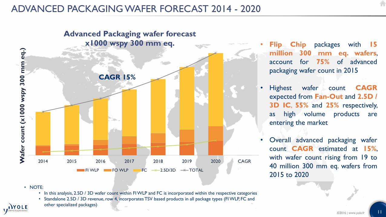
ADVANCED PACKAGING WAFER FORECAST 2014 - 2020
• Flip Chip packages with 15
million 300 mm eq. wafers,
account for 75% of advanced
packaging wafer count in 2015
• Highest wafer count CAGR
expected from Fan-Out and 2.5D /
3D IC, 55% and 25% respectively,
as high volume products are
entering the market
• Overall advanced packaging wafer
count CAGR estimated at 15%,
with wafer count rising from 19 to
40 million 300 mm eq. wafers from
2015 to 2020
• NOTE:
• In this analysis, 2.5D / 3D wafer count within FI WLP and FC is incorporated within the respective categories
• Standalone 2.5D / 3D revenue, row 4, incorporates TSV based products in all package types (FI WLP, FC and
other specialized packages)
CAGR 15%
2014 2015 2016 2017 2018 2019 2020 CAGRWafe
r co
un
t (x
1000 w
spy 3
00 m
m e
q.)
Advanced Packaging wafer forecast
x1000 wspy 300 mm eq.
FI WLP FO WLP FC 2.5D/3D TOTAL

12©2016 | www.yole.fr
ADVANCED PACKAGING REVENUE FORECAST 2014 vs. 2020
FI WLP
4 594
15%
FO WLP
2 391
8%
FC
23 034
77%
FI WLP
2 946
15% FO WLP
174
1%
FC
17 073
84%
TOTAL 2014
20,2 $B
TOTAL 2020
30 $B
• Due to faster growth, FO
WLP is expected to
decrease market shares of
Flip Chip
• FO WLP is expected to rise
from 1% advanced packaging
market share in 2014 to 8%
in 2020
• While maintaining growth,
from 2014 to 2020 Flip Chip
market share is expected to
drop from 84% to 77% while
FI WLP will remain at 15%
• NOTE: 2.5D / 3D revenue found within FI WLP and FC is incorporated within the respective categories

13©2016 | www.yole.fr
PLAYERS WITH ADVANCED PACKAGING CAPABILITY
Partial list
Key players in China with advanced packaging capability
Millenium Microtech Co. Ltd, bought
by FlipChip International, is now part of
Huatian. TianShui Huatian Technology
Co., LTD (“Huatian”) acquired FlipChip
International LLC and its subsidiary,
Millennium Microtech (Shanghai) Co.,
LTD, on Apr.1, 2015.
IDM
14©2016 | www.yole.fr
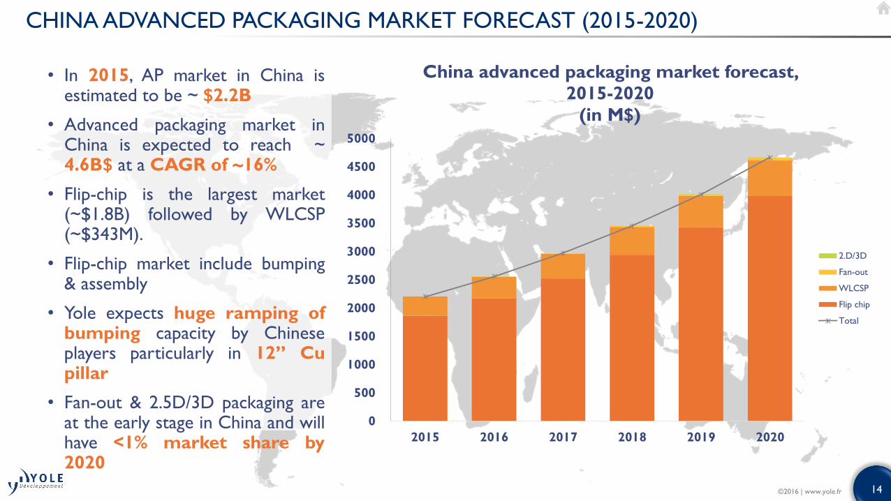
CHINA ADVANCED PACKAGING MARKET FORECAST (2015-2020)
• In 2015, AP market in China isestimated to be ~ $2.2B
• Advanced packaging market inChina is expected to reach ~4.6B$ at a CAGR of ~16%
• Flip-chip is the largest market(~$1.8B) followed by WLCSP(~$343M).
• Flip-chip market include bumping& assembly
• Yole expects huge ramping ofbumping capacity by Chineseplayers particularly in 12” Cupillar
• Fan-out & 2.5D/3D packaging areat the early stage in China and willhave <1% market share by2020
0
500
1000
1500
2000
2500
3000
3500
4000
4500
5000
2015 2016 2017 2018 2019 2020
China advanced packaging market forecast,
2015-2020
(in M$)
2.D/3D
Fan-out
WLCSP
Flip chip
Total

15©2016 | www.yole.fr
ADVANCED PACKAGING MARKET IN CHINA – THE RISE OF CHINA
0
5000
10000
15000
20000
25000
30000
35000
2015 2016 2017 2018 2019 2020
Advanced packaging market forecast, 2015-2020
(Global vs China) – Market (M$)
Global
China
• AP in China is expected to growat double CAGR (~16%)compared to 7% globally
• The growth in China AP is led byJCET/STATSChipPAC, Huatian,NFME, and China WLCSP
• After acquiring STATSChipPAC,JCET is the #4 OSAT in revenueglobally
• Global OSATs like Amkor and SPILare investing in the AP capability oftheir Chinese operations
• Amkor China (Shanghai) operationis the Amkor’s second-largestfactory by revenue"

16©2016 | www.yole.fr
ADVANCED PACKAGING - KEY MESSAGES
• Scaling of transistors is getting more and more complex. To enable solutions, focusis therefore on Advanced Packaging throught different platforms
• Advanced Packaging will keep growing in the next five years from 20B$ up to 30B$in 2020.
• Fan Out packaging is expected to have the fastest growth with a CAGR of 55%from 2015 to 2020 mainly due to its adoption in consumer market (Apple entry)
• 3D is getting is era in the high end application. Stacked memories will become key forhigh performance devices
• Advanced Packaging in China will grow faster (16%) compare to the global trendhowever emerging platforms are still at the early stage (3D, Fan Out.)

17©2016 | www.yole.fr
PRESENTATION OUTLINE
oStatus of Advanced Packaging• Market Dynamics, Drivers & Evolution of Semiconductor Packaging
• Advanced Packaging Platforms
• Market forecasts
• What about China?
• Key messages
oAn closer look on Fan-Out Packaging• Fan Out Applications
• Market trends
• Key messages
oConclusions
• Summary

18©2016 | www.yole.fr
KEY APPLICATIONS
Different applications with different needs and characteristics (Density, package size)
Codec
DC-DC
Wifi
BB
PMU/PMIC
RF
Application
Processors (APE)
+ BB
APE+DRAM
GPU, CPU + Memory
(Wide IO, etc…)
High Bandwidth
Memories
FPGA
Processors + Memories
IO density (IO/mm/layer)
200
100
1
2x2 5x5 10x10 15x15 20x20 >20x20 >>20x20 Package size
(mmxmm)
MEMS
CMOS Image Sensors
Display Drivers
10
>>200

19©2016 | www.yole.fr
MEMS
CMOS Image Sensors
Display Drivers
Codec
DC-DC
Wifi
BB
PMU/PMIC
RF
Application
Processors
(APE) + BB
APE+DRAM
GPU,CPU+Memory
(Wide IO, etc…)
High Bandwith Memories
FPGA
Processors+Memories
FAN-OUT APPLICATIONS
Potential applications for Fan-Out: Where does Fan-Out fit and how?
Single Chip FOWLP
Multi-Chip
FO PoP with TMV
FO SiP
Multi-Chip
FO PoP with TMV
IO count10000
1000
100
2x2 5x5 10x10 15x15 20x20 >20x20 >>20x20
Package
size
(mmxmm)

20
FAN-OUT APPLICATIONS
Where can we and will we find Fan-Out? Some examples below
Orange: Devices that can be found in
FOWLP packages today
Green: Devices that could be found
in the future in FOWLPGrey: Devices that will likely remain
on WLCSP or flip-chip package or
move to 3DIC or Embedded die
Apple iPhone 7 (2016)A10 APE – InFO package (TSMC)
Samsung Galaxy S7 (2016)Qualcomm Audio Codec
WCD9335 – eWLB package
(Nanium/STATS ChipPAC)
Bosch MRR1Plus Radar (2015)Infineon RASIC™ (77GHz RADAR System
IC Chipset) – eWLB Package
BK Ultrasound Sonic Window (2015)Multichip Module – eWLB Package (Nanium)
BasebandSpreadtrumSC8502
Intel-Mobile/InfineonPMB7900, PMB9810, PMB9801
RFSpreadtrumSC8502
Intel-Mobile/InfineonPMB5712, PMB5726 Power Management
MarvellPM820
SpreadtrumSC2712A
Continental ARS400 Radar (2015)NXP MR2001 (77GHz multichannel
RADAR) – RCP Package
©2016 | www.yole.fr | Yole Développement

21©2016 | www.yole.fr
APE
FAN-OUT APPLICATIONS
Example of Qualcomm’s Audio Codec
WCD9335 – eWLB package
Die size: 3.6x3.6mm² Package size:
4.18x3.91mm² 113 balls bumped
Source: System + Consulting
Audio codecRF in automotive
TSMC’s InFO for Apple A10Example of Infineon’s Transceiver
and Receiver in Bosch MRR1 Plus
Radar – eWLB packages
Source: System + Consulting
2012 2013 20142011 2015 2016

22©2016 | www.yole.fr
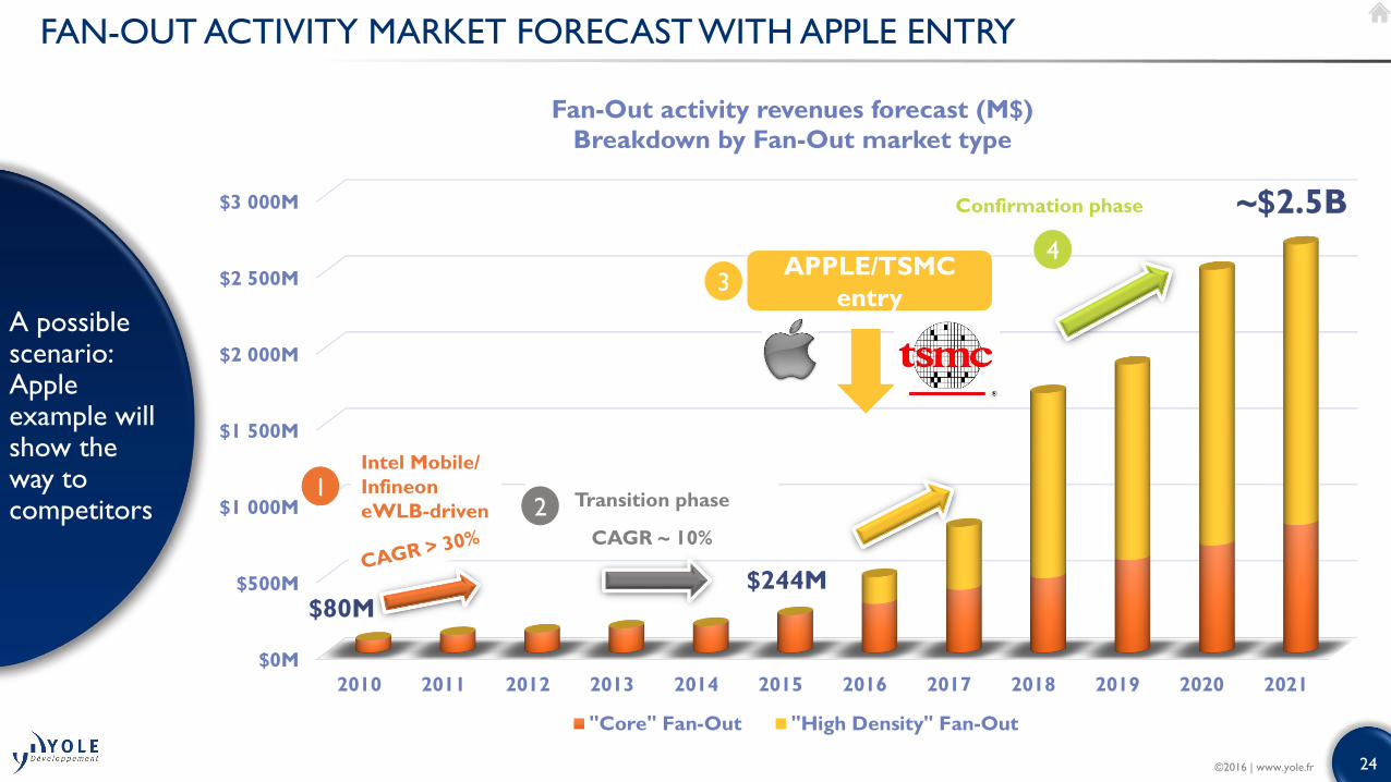
FAN-OUT MARKET STATUS
Entering a new era…
• A confirmed ramp-up and high expectations for a promising“core” market.
• A high potential for “High-Density” Fan-Out
Fan-Out market has reached a turning point • Is there a Fan-Out Bubble?
• Fan-Out is the new trendy platform the industry is focusing on…
• … but main part of Fan-Out Market for 2016 will be associated to only one product

23©2016 | www.yole.fr
IS THERE A FAN-OUT BUBBLE?
Fan-Out market risks
• Heavy competition pushed by substrates manufacturers may limit its success
High expectations induce risks
• Fan-Out market may not be not as sustainable as it seems: Few players dependency
24©2016 | www.yole.fr
$0M
$500M
$1 000M
$1 500M
$2 000M
$2 500M
$3 000M
2010 2011 2012 2013 2014 2015 2016 2017 2018 2019 2020 2021
Fan-Out activity revenues forecast (M$)
Breakdown by Fan-Out market type
"Core" Fan-Out "High Density" Fan-Out
FAN-OUT ACTIVITY MARKET FORECAST WITH APPLE ENTRY
A possible scenario: Apple example willshow the way to competitors
APPLE/TSMC
entry
CAGR ~ 10%
Intel Mobile/
Infineon
eWLB-drivenTransition phase
12
3
4
~$2.5B
$80M$244M
Confirmation phase

25©2016 | www.yole.fr
FAN-OUT PACKAGING 2015 REVENUES MARKET SHARES (IN M$)
2015 FOWLP marketstatus shows a domination of twoplayers usingeWLB
59%25%
16%
Main products:
- eWLB single die packages for
Mobile and Wireless BB
and Wireless SoC, RF, PMIC
- MCP/SiP products for Mobile
(PMU), Industrial, Medical and
Security applications
eWLB products mainly
for
- Mobile and Wireless
BB and Wireless SoC
- PMU/PMIC
- RF
Others
TOTAL 2015
$244M

26©2016 | www.yole.fr
37%
12%
35%
16%
FAN-OUT PACKAGING 2016 REVENUES MARKET SHARES (IN M$)
2016 Fan-Out marketstatus shows TSMC entry and inFOtake over
TOTAL 2016
$492M
2016: Apple A10 entry with TSMC info will change the Fan-Out market landscape!
Others

27©2016 | www.yole.fr
FAN-OUT TECHNOLOGIES VS OTHER TECHNOLOGIES
A subtile trade-off between cost, performance and integration, case by case
DRAMDRAM
• Solution supplied by TSMC for Apple A10
Fan-Out PoP Flip Chip PoP Embedded die PoP
• Solution supplied by Samsung for its Exynos 8
• Solution supplied by Shinko for Qualcomm’s Snapdragon 820

28©2016 | www.yole.fr
FAN-OUT PACKAGING: AN EVOLUTION NOT A REVOLUTION
• Fan-Out packaging has numerous added values (form factor, electrical performance,…)
• Fan-Out Packaging is already adopted by the industry and will keep growing
• Following that success numerous players entered the game and provided newtechnologies inducing some confusion on what is “Fan-Out”
• Apple entry using TSMC InFo has changed the game and may have created a bubble…
• ~150$M loss is expected for substrate manufacturers in the 2 coming years.
• … but the market will enlarge anyway since it has high potential in telecom, medical andautomotive

29©2016 | www.yole.fr
PRESENTATION OUTLINE
oStatus of Advanced Packaging• Market Dynamics, Drivers & Evolution of Semiconductor Packaging
• Advanced Packaging Platforms
• Market forecasts
• What about China?
• Key messages
oAn closer look on Fan-Out Packaging• Fan Out Applications
• Market trends
• Key messages
oConclusions
• Summary

30©2016 | www.yole.fr
CONCLUSION: ADVANCED PACKAGING OVERVIEW
• Fan-in – stable growth, still driven by low cost and introduction of new
consumer applications (IoT) requiring low cost and pin count
• Flip-chip – will continue to grow, but expected to loose overall market
share to platforms such as WLCSP, Fan-Out and 3DIC. Cu Pillar will
continue to be the dominant flip chip metallurgy
• Fan-Out – very promising platforms already established in production.
Currently using wafer infrastructure, may move to panel manufacturing in
near future. Fan-out could be a disruptive technology for consumer
applications
• 2.5D & 3DIC – finally in production and adoption expected to further
grow. After MEMS and CIS, Memory will be the next segment to see the
growth and adoption of TSV.
• Advanced Substrates / SiP – enabling increased functionality solutions,
is a high interest packaging approach, especially driven by IoT (wearables)
RF applications and automotive
31©2016 | www.yole.fr
CONLUSION: ADVANCED PACKAGING OVERVIEW
ADVANCED PACKAGING is KEY
for the FUTURE!
THANKYOU for your attention!

32©2016 | www.yole.fr
INFORMATION EXTRATED FROMYOLE REPORTS
+ Several reports from System Plus Consulting & Knowmade
http://www.i-micronews.comMeet with the analysts at our BOOTH #850

Yole DéveloppementCompany Presentation
Light festival in Lyon
34
MEMS &
Sensors
LED
Compound
Semi.
Imaging
RF
MedTech
Manufacturing
Advanced Packaging
Batteries / Energy
Management
Power
Electronics
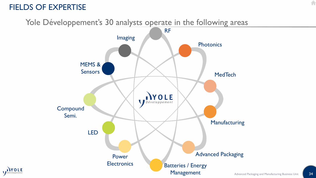
FIELDS OF EXPERTISE
Yole Développement’s 30 analysts operate in the following areas
Advanced Packaging and Manufacturing Business Unit
Photonics

35
4 BUSINESS MODELS
o Consulting and Analysis
• Market data & research, marketing analysis
• Technology analysis
• Strategy consulting
• Reverse engineering & costing
• Patent analysis
www.yole.fr
o Reports
• Market & Technology reports
• Patent Investigation and patent infringement risk analysis
• Teardowns & Reverse Costing Analysis
• Cost Simulation Tool
www.i-Micronews.com/reports
o Financial services
• M&A (buying and selling)
• Due diligence
• Fundraising
• Maturation of companies
• IP portfolio management & optimization
www.yolefinance.com
www.bmorpho.com
o Media
• i-Micronews.com website
• @Micronews e-newsletter
• Communication & webcast services
• Events
www.i-Micronews.com
Advanced Packaging and Manufacturing Business Unit

36
A GROUP OF COMPANIES
Market,
technology and
strategy
consulting
www.yole.fr
M&A operations
Due diligences
www.yolefinance.com
Innovation and business maker
www.bmorpho.com
Manufacturing costs analysis
Teardown and reverse engineering
Cost simulation tools
www.systemplus.fr
IP analysis
Patent assessment
www.knowmade.fr
Advanced Packaging and Manufacturing Business Unit

37
OUR GLOBAL ACTIVITY
Advanced Packaging and Manufacturing Business Unit


