

SiC Power Device Development for Clean Energy ApplicationsJeffrey B. CasadyChief Technology Officer & VP Business Development
Sept 30, 2008
Funded by the Energy Storage Systems Program of the U.S. Department Of Energy (DOE/ESS) through the Small Business Innovation Research (SBIR) program and managed by Sandia National Laboratories (SNL). Sandia is a multi-program laboratory operated by Sandia Corporation, a Lockheed Martin Company, for the United States Department of Energy’s National Nuclear Security Administration, under contract DE-AC04-94AL85000

www.semisouth.com 2
SemiSouth Laboratories is a clean energy enablerspecializing in the design & manufacture of silicon carbide (SiC) Devices and
power modules used to harvest and transfer power in renewable energy systems,telecom server farms & hybrid electric vehicles.
Solar
Wind
HEV
Servers
Business Strategy

www.semisouth.com 3
Corporate Snapshot
• First & only company to offer cost effective SiC technology for power management• Corporate & Sales Offices: Austin, Texas• Manufacturing Facility: Starkville, Mississippi
• Brick-and-Mortar revenue capability = $60M annualized
• Total Employees: 50 employees
• Ownership: Privately owned by strategic investors (II-VI, Schneider Electric Ventures), venture capital, and employees

www.semisouth.com 4
Experienced Fab Personnel
Multiple Etch & PECVD systems
Multiple Metal systems
Significant Investment in equipment being qualified for production NOW
~25% cycle time reduction expected

www.semisouth.com 5
It’s three to ten times better than silicon for power efficiency!It enables system performance which is IMPOSSIBLE in Si!
Why Silicon Carbide?

www.semisouth.com 6
DC voltage (400 V to 2 kV)
DC voltage (400 V to 2 kV)
AC voltage back to grid for distribution and storage
AC voltage to home
AC to battery in EV
SILICON CARBIDE ENABLES SOLAR, WIND, EV inverters– 50% reduction in energy distribution losses and reduced equipment costs
Inverters (DC-AC)
On-board DC from battery to
AC in motor
SiC Enables Clean Energy

www.semisouth.com 7
SemiSouth Near-term ProductPart Number SJEP120R200 SJEP120R125 SJEP120R63 SJEP120R32
Package
Id (cont) 5A 15A 30A 50A
Rds (0n) 200 mOhm 125 mOhm 63 mOhm 32 mOhm
Samples Q4 08 Now Q3 08 Q4 08
1200 V Class Products for power level applications from 300 W to 30 kW approaching commercialization
SemiSouth offers normally-off SiC JFET’s (OFFET™) and normally-on SiC JFET’s

www.semisouth.com 8
JFET Reliability (Pre-Qual)
2.52.62.72.82.93.03.13.23.33.43.5
0 1000 2000 3000 4000 5000Thermal stress time (hours)
Ron
-sp
(m .c
m2 )
Temperature = 250 °C, VGS = 3V
1200 V Class Products are Unipolar Devices and VERY RELIABLE

www.semisouth.com 9
SemiSouth Progress in EV
6 kW drive demo demonstrated NOW – scaling to automotive power levels (60-200 kW)Dramatic improvements in power density, efficiency, and thermal management
6 kW electric drive demo with SemiSouth SiC transistors and diodes

www.semisouth.com 10
SemiSouth Progress in SolarSiC OFFET™ in Solar Inverter
96.0
96.5
97.0
97.5
98.0
98.5
99.0
0 500 1000 1500 2000
AC-Power / W
Effic
ienc
y / % 25A/1200V Si-IGBT
25A/1200 V SiC-JFET
20
30
40
50
60
70
80
90
0 500 1000 1500 2000 2500AC-Power / W
FET
Tem
pera
ture
/ °C
25A/1200 V Si-IGBT25A/1200 V SiC-JFET
Third Party Evaluation of 2 kW Inverter16 kHz, 350 V DC Input, module1.6% improvement over Silicon IGBT
98.8%
www.semisouth.com 11
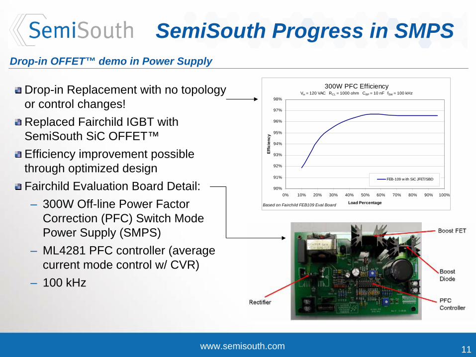
Drop-in Replacement with no topology or control changes!Replaced Fairchild IGBT with SemiSouth SiC OFFET™Efficiency improvement possible through optimized designFairchild Evaluation Board Detail:– 300W Off-line Power Factor
Correction (PFC) Switch Mode Power Supply (SMPS)
– ML4281 PFC controller (average current mode control w/ CVR)
– 100 kHz
SemiSouth Progress in SMPSDrop-in OFFET™ demo in Power Supply
300W PFC EfficiencyVin = 120 VAC RCL = 1000 ohm CBP = 10 nF fSW = 100 kHz
90%
91%
92%
93%
94%
95%
96%
97%
98%
0% 10% 20% 30% 40% 50% 60% 70% 80% 90% 100%
Load Percentage
Effic
ienc
y
FEB-109 w ith SiC JFET/SBD
Based on Fairchild FEB109 Eval Board

www.semisouth.com 12
Basal Plane Dislocations (BPD)Impact Bipolar SiC devicesBipolar Devices in SiC required above 3 kVBPD’s lead to stacking faultsStacking faults lead to device instability
SemiSouth eliminated BPD’s in Phase I from DOE (2007-08)!
SemiSouth Progress in HVMaterial Scaling for High Voltage Devices (> 3 kV) – Funded by DOE Phase I
DOE Phase I – Grant # DE-FG02-07ER84693; Thanks to Dr. Imre Gyuk, DOE Energy Storage Program and Dr. Stan Atcitty, Sandia National Laboratories for support.
www.semisouth.com 13
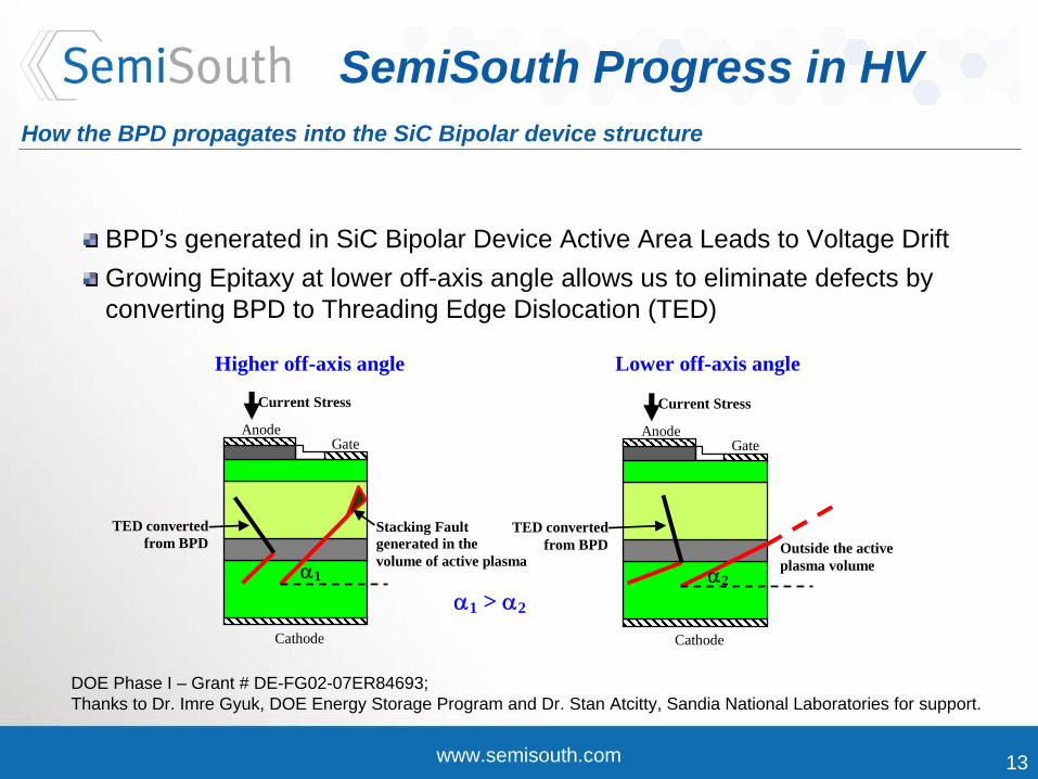
BPD’s generated in SiC Bipolar Device Active Area Leads to Voltage DriftGrowing Epitaxy at lower off-axis angle allows us to eliminate defects by converting BPD to Threading Edge Dislocation (TED)
SemiSouth Progress in HVHow the BPD propagates into the SiC Bipolar device structure
Anode Gate
Cathode
Stacking Faultgenerated in the volume of active plasma
TED converted from BPD
Current Stress
Anode Gate
Cathode
TED converted from BPD
Current Stress
Outside the activeplasma volume
Higher off-axis angle Lower off-axis angle
1 2
1 > 2
DOE Phase I – Grant # DE-FG02-07ER84693; Thanks to Dr. Imre Gyuk, DOE Energy Storage Program and Dr. Stan Atcitty, Sandia National Laboratories for support.

www.semisouth.com 14
Nomarski image (left) and UVPL image (right) of an 11 um thick epitaxy layer (1.5 kV epitaxy structure) with no BPD’sSemiSouth has demonstrated 100 um thick epitaxy layers (20 kV epi structure) in other funded efforts
SemiSouth Progress in HVSemiSouth’s SiC epitaxy structure with ZERO BPD! (DOE Phase I Result!)
200µm
2° off-axis Etch Pit Density (EPD)Avg / Min / Max (cm-2)
Basal Plane DefectsAvg / Min / Max (cm-2)
Virgin Substrate 4.61e4 / 2.15e3 / 1.72e5 1.27e3 / 0 / 7.15e3
Post SemiSouth Epi 6.66e4 / 3.58e3 / 3.12e5 None
Measurement results courtesy of Naval Research Lab (UVPL), SiCrystal (KOH etch), and Mississippi State University (KOH &PL)
DOE Phase I – Grant # DE-FG02- 07ER84693; Thanks to Dr. Imre Gyuk, DOE Energy Storage Program and Dr. Stan Atcitty, Sandia National Laboratories for support.

www.semisouth.com 15
Summary
• SemiSouth is only company offering normally-off (OFFET™) or normally-on JFET
• Third party measurement of 98.8% peak efficiency in solar inverter (Fraunhofer) using SemiSouth OFFET™
• Strong SiC Epitaxy Materials Development (funded by DOE & others) is allowing SemiSouth to scale up device structures above 3 kV through elimination of BPD
• Further Development needed to push into higher power class for Wind Energy (MW) and other classes requiring high-power, reliable bipolar structures


